APA2106QBCD, 规格书,Datasheet 资料
GBPC3506W;GBPC3502;GBPC3510W;GBPC3510;GBPC1506;中文规格书,Datasheet资料

The following includes registered and unregistered trademarks and service marks, owned by Fairchild Semiconductor and/or its global subsidiaries, and is notAccuPower¥Auto-SPM¥Build it Now¥CorePLUS¥CorePOWER¥CROSSVOLT¥CTL¥Current Transfer Logic¥DEUXPEED®Dual Cool™ EcoSPARK®EfficientMax¥ESBC¥®Fairchild®Fairchild Semiconductor®FACT Quiet Series¥FACT®FAST®FastvCore¥FETBench¥FlashWriter®*FPS¥F-PFS¥FRFET®Global Power Resource SMGreen FPS¥Green FPS¥ e-Series¥G max¥GTO¥IntelliMAX¥ISOPLANAR¥MegaBuck¥MICROCOUPLER¥MicroFET¥MicroPak¥MicroPak2¥MillerDrive¥MotionMax¥Motion-SPM¥OptoHiT™OPTOLOGIC®OPTOPLANAR®®PDP SPM™Power-SPM¥PowerTrench®PowerXS™Programmable Active Droop¥QFET®QS¥Quiet Series¥RapidConfigure¥¥Saving our world, 1mW/W/kW at a time™SignalWise¥SmartMax¥SMART START¥SPM®STEALTH¥SuperFET¥SuperSOT¥-3SuperSOT¥-6SuperSOT¥-8SupreMOS®SyncFET¥Sync-Lock™®*The Power Franchise®TinyBoost¥TinyBuck¥TinyCalc¥TinyLogic®TINYOPTO¥TinyPower¥TinyPWM¥TinyWire¥TriFault Detect¥TRUECURRENT¥*P SerDes¥UHC®Ultra FRFET¥UniFET¥VCX¥VisualMax¥XS™* Trademarks of System General Corporation, used under license by Fairchild Semiconductor.DISCLAIMERFAIRCHILD SEMICONDUCTOR RESERVES THE RIGHT TO MAKE CHANGES WITHOUT FURTHER NOTICE TO ANY PRODUCTS HEREIN TO IMPROVE RELIABILITY, FUNCTION, OR DESIGN. FAIRCHILD DOES NOT ASSUME ANY LIABILITY ARISING OUT OF THE APPLICATION OR USE OF ANY PRODUCT OR CIRCUIT DESCRIBED HEREIN; NEITHER DOES IT CONVEY ANY LICENSE UNDER ITS PATENT RIGHTS, NOR THE RIGHTS OF OTHERS. THESE SPECIFICATIONS DO NOT EXPAND THE TERMS OF FAIRCHILD’S WORLDWIDE TERMS AND CONDITIONS, SPECIFICALLY THE WARRANTY THEREIN, WHICH COVERS THESE PRODUCTS.LIFE SUPPORT POLICYFAIRCHILD’S PRODUCTS ARE NOT AUTHORIZED FOR USE AS CRITICAL COMPONENTS IN LIFE SUPPORT DEVICES OR SYSTEMS WITHOUT THE EXPRESS WRITTEN APPROVAL OF FAIRCHILD SEMICONDUCTOR CORPORATION.As used herein:1. Life support devices or systems are devices or systems which, (a) areintended for surgical implant into the body or (b) support or sustain life,a nd (c) whose fa ilure to perform when properly used in a ccorda ncewith instructions for use provided in the la beling, ca n be rea sona bly expected to result in a significant injury of the user. 2. A critical component in any component of a life support, device, orsystem whose fa ilure to perform ca n be rea sona bly expected to cause the failure of the life support device or system, or to affect its safety or effectiveness.ANTI-COUNTERFEITING POLICYFairchild Semiconductor Corporation's Anti-Counterfeiting Policy. Fairchild's Anti-Counterfeiting Policy is also stated on our external website, , under Sales Support.Counterfeiting of semiconductor parts is a growing problem in the industry. All manufacturers of semiconductor products are experiencing counterfeiting of their parts. Customers who inadvertently purchase counterfeit parts experience many problems such as loss of brand reputation, substandard performance, failed applications, and increased cost of production and manufacturing delays. Fairchild is taking strong measures to protect ourselves and our customers from the proliferation of counterfeit parts. Fairchild strongly encourages customers to purchase Fairchild parts either directly from Fairchild or from Authorized Fairchild Distributors who are listed by country on our web page cited above. Products customers buy either from Fairchild directly or from Authorized Fairchild Distributors are genuine parts, have full traceability, meet Fairchild's quality standards for handling and storage and provide access to Fairchild's full range of up-to-date technical and product information. Fairchild and our Authorized Distributors will stand behind all warranties and will appropriately address any warranty issues that may arise. Fairchild will not provide any warranty coverage or other assistance for parts bought from Unauthorized Sources. Fairchild is committed to combat this global problem and encourage our customers to do their part in stopping this practice by buying direct or from authorized distributors.PRODUCT STATUS DEFINITIONSDefinition of TermsDatasheet Identification Product Status Definition分销商库存信息:FAIRCHILDGBPC3506W GBPC3502GBPC3510W GBPC3510GBPC1506GBPC2502 GBPC2506GBPC3504GBPC12005 GBPC1202W GBPC1202GBPC1210 GBPC1201GBPC1204W GBPC1206W GBPC1210W GBPC1206GBPC1208 GBPC1204GBPC1201W GBPC15005 GBPC1501GBPC1510W GBPC1506W GBPC1501W GBPC1504W GBPC1510 GBPC1508GBPC1502W GBPC1502 GBPC1508W GBPC1504GBPC15005W GBPC2501GBPC2508GBPC25005 GBPC2504GBPC3504W GBPC3508W GBPC3501W GBPC35005W GBPC3502W GBPC2510GBPC3508GBPC3501 GBPC35005GBPC3506GBPC2501W GBPC2502W GBPC25005W GBPC2508W GBPC2506W GBPC2510W。
欧姆龙AQY210光电继电器系列产品说明书
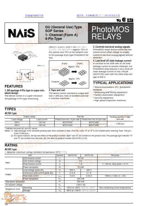
441243GU (General Use) TypeSOP Series1- Channel (Form A) 4-Pin Typemm inch4.4±0.2.173±.0082.1±0.2.083±.0084.3±0.2.169±.008FEATURES1. SO package 4-Pin type in super min-iature designThe device comes in a super-miniature SO package 4-Pin type measuring(W)4.3 × (L)4.4 × (H)2.1 mm (W).169 × (L).173 × (H).083 inch —approx. 70% of the volume and 70% of the footprint size of SO package 6-pin type PhotoMOS Re-lays.2. Tape and reelThe device comes standard in a tape and reel (1,000 pcs./reel) to facilitate automat-ic insertion machines.Volume(4-pin)(6-pin)Approx. 70%FootprintApprox. 70%3. Controls low-level analog signals PhotoMOS relays feature extremely low closed-circuit offset voltage to enable control of low-level analog signals without distortion.4. Low-level off state leakage current In contrast to the SSR with an off state leakage current of several milliamps, the PhotoMOS relay features a very small off state leakage current of only 100 pA (AQY214S) even with the rated load volt-age of 400 V .TYPICAL APPLICATIONS• T elecommunications (PC, Electoronic Notepad)• Measuring and T esting equipment • Factory Automation Equipment • Security equipment• High speed inspection machinesTYPESAC/DC type* Indicate the peak AC and DC values.(1)Tape package is the standard packing style. Also available in tube. (Part No. suffix "X" or "Z" is not needed when ordering; T ube: 100 pcs.;Case: 2,000 pcs.)(2)For space reasons, the top two letters of the product number "AQY" and "S" are omitted on the product seal. The package type indicator "X"and "Z" are omitted from the seal. (Ex. the label for product number AQY210S is 210).Output rating*Part No.Packing quantity in tapeand reelLoad voltageLoad current Picked from the 1/2-pin side Picked from the 3/4-pin side350 V 120 mA AQY210SX AQY210SZ 1,000 pcs.400 V100 mAAQY214SX AQY214SZRATINGAC/DC type1. Absolute maximum ratings (Ambient temperature: 25 ° C 77 ° F )ItemSymbol AQY210SAQY214SRemarksInputLED forward current I F 50 mA LED reverse voltageV R 3 V Peak forward current I FP 1 A f = 100 Hz, Duty factor = 0.1%Power dissipationP in 75 mWOutputLoad voltage (peak AC)V L 350 V 400 V Continuous load current (peak AC)I L 0.12 A 0.1 A Peak load current I peak 0.3 A0.24 A 100ms (1 shot), V L = DCPower dissipationP out 300 mW T otal power dissipation P T 350 mW I/O isolation voltageV iso 1,500 V ACT emperture limitsOperatingTopr –40 ° C to +85 ° C –40 ° F to +185 ° F Non-condensing at low temperaturesStorageTstg–40 ° C to +100 ° C –40 ° F to +212 °FPhotoMOS RELAYS查询AQY210供应商捷多邦,专业PCB打样工厂,24小时加急出货AQY21 r S452. Electrical characteristics (Ambient temperature: 25 ° C 77 ° F )Note: Recommendable LED forward current IF = 5mA. For type of connection, see page 31.*Turn on/T urn off times For Dimensions, see Page 28.s For Schematic and Wiring Diagrams, see Page 31. s For Cautions for Use, see Page 36.ItemSymbol AQY210SAQY214SRemarks InputLED operate currentTypical I Fon 0.9 mA I L = Max.Maximum 3 mA LED turn off current Minimum I Foff 0.4 mA I L = Max.Typical 0.85 mALED dropout voltage Typical V F1.14 V (1.25 V at IF = 50 mA)I F = 5 mA Maximum 1.5 V OutputOn resistanceTypical Ron17 Ω 25 Ω I F = 5 mA IL = Max.Within 1 s on time Maximum 25 Ω35 ΩOff state leakage current Maximum ILeak 1 µ AI F = 0I L = Max.TransfercharacteristicsTurn on time*T ypical T on 0.23 ms0.21 ms I F = 5 mAI L = Max.Maximum 0.5 ms Turn off time*Typical T off 0.04 ms I F = 5 mA I L = Max.Maximum 0.2 ms I/O capacitanceMaximum C iso1.5 pF f = 1 MHz V B = 0Initial I/O isolation resistanceMinimumRiso1,000 M Ω500 V DCInputOutput10%90%REFERENCE DATA1. Load current vs. ambient temperature char-acteristicsAllowable ambient temperature:–40 ° C to +85 ° C–40 ° F to +185 ° F2. On resistance vs. ambient temperature char-acteristicsMeasured portion: between terminals 3 and 4;LED current: 5 mA; Load voltage: Max. (DC);Continuous load current: Max. (DC)3. T urn on time vs. ambient temperature char-acteristicsLED current: 5 mA; Load voltage: Max. (DC);Continuous load current: Max. (DC)60801001202040Ambient temperature, °C L o a d c u r r e n t , m A 01020304050Ambient temperature, °CO n r e s i s t a n c e , Ω1.01.52.50.52.03.0Ambient temperature, °CT u r n o n t i m e , m sAQY21 r S4. Turn off time vs. ambient temperature char-acteristicsLED current: 5 mA; Load voltage: Max. (DC);Continuous load current: Max. (DC)5. LED operate current vs. ambient tempera-ture characteristicsSample: All types; Load voltage: Max. (DC);Continuous load current: Max. (DC)6. LED turn off current vs. ambient temperature characteristicsSample: All types; Load voltage: Max. (DC);Continuous load current: Max. (DC)Ambient temperature, °C T u r n o f f t i m e , m s1234–4050–202040608085Ambient temperature, °C L E D o p e r a t e c u r r e n t , m A1234–4050–202040608085Ambient temperature, °CL E D t u r n o f f c u r r e n t , m A。
RB521G-30-TP;中文规格书,Datasheet资料

RB521G-30100 mASchottky Barrier Diode30 VoltsFeatures• High Reliability•Low Reverse Current and Low Forward Voltage. www.mccsemi .comTMMicro Commercial Components• Lead Free Finish/RoHS Compliant ("P" Suffixdesignates RoHS Compliant. See ordering information)Revision: A 2011/01/01 omp onents 20736 Marilla Street Chatsworth! "# $ % ! "#1 of 3• Epoxy meets UL 94 V-0 flammability rating • Moisture Sensitivity Level 1/RB521G-30www.mccsemi .comRevision: A 2011/01/01Micro Commercial Components2 of 3/Revision: A 2011/01/01Micro Commercial Componentswww.mccsemi .com3 of 34DevicePackingPart Number-TP Tape&Reel: 8Kpcs/ReelOrdering Information :***IMPORTANT NOTICE***Micro Commercial Components Corp. reserve s the right to make changes without further notice to any product herein to make corrections, modifications , enhancements , improvements , or other changes . Micro Commercial Components Corp . does not assume any liability arising out of the application or use of any product described herein; neither does it convey any license under its patent rights ,nor the rights of others . The user of products in such applications shall assume all risks of such use and will agree to hold Micro Commercial Components Corp . and all the companies whose products are represented on our website, harmless against all damages.***LIFE SUPPORT***MCC's products are not authorized for use as critical components in life support devices or systems without the express writtenapproval of Micro Commercial Components Corporation.***CUSTOMER AWARENESS***Counterfeiting of semiconductor parts is a growing problem in the industry. Micro Commercial Components (MCC) is taking strong measures to protect ourselves and our customers from the proliferation of counterfeit parts. MCC strongly encourages customers to purchase MCC parts either directly from MCC or from Authorized MCC Distributors who are listed by country on our web page cited below . Products customers buy either from MCC directly or from Authorized MCC Distributors are genuine parts, have full traceability, meet MCC's quality standards for handling and storage. MCC will not provide any warranty coverage or other assistance for parts bought from Unauthorized Sources. MCC is committed to combat this global problem and encourage our customers to do their part in stopping this practice by buying direct or from authorized distributors./分销商库存信息: MICRO-COMMERICAL-CO RB521G-30-TP。
SI2302-TP;中文规格书,Datasheet资料

Revision: A
/
3 of 5
2011/01/01
VGS, Gate to Source Voltage (V) ID, Drain Current (A)
VTH, Normalized Gate-Source Threshold Voltage
RDS(ON), Normalized RDS(ON), On-Resistance(Ohms)
IS, Source-drain current (A)
ID, Drain Current (A)
SI2302
10 25 C
Maximum Ratings @ 25OC Unless Otherwise Specified
Symbol VDS ID IDM VGS
PD R©JA
TJ
TSTG
Parameter Drain-source Voltage Drain Current-Continuous Drain Current-Pulsed a Gate-source Voltage
MCC
TM
Micro Commercial Components
5 VDS=10V ID=3.6A
4
3
2
1
0
0
2
4
6
Qg, Total Gate Charge (nC)
Figure 7. Gate Charge
VDD
RL VIN
D
VOUT
VGS
RGEN G
S
Figure 9. Switching Test Circuit
ZS205 ZS210规格书 datasheet 深圳市高胜科研电子有限公司
DATA SHEETZS210/ZS205高精度恒流/恒压原边PWM功率开关版本号:V1.0一、概述ZS205/ZS210是一颗应用于小功率AC/DC充电器和电源适配器的高性能离线式脉宽调制控制器。
该芯片使用原边取样和调整的拓扑结构,进行精确的恒流、恒压控制,可以省去一般应用中的光耦与TL431。
在恒流模式下,输出功率与输出电流可由CS脚外接的取样电阻Rs设定;在恒压模式下,芯片内置恒压采样电路以及高精度的误差比较器可以保证较高的整体转换效率。
此外,芯片内置有线压降补偿,保证了空载到满载条件下的输出电压精度。
该芯片还有极低的静态工作电流,芯片待机功耗低于100mW。
ZS205/ZS210提供上电软启动功能与各种可自恢复的保护功能,包括逐周期限流保护(OCP),VDD过压保护(OVP),VDD过压箝位,欠压保护(UVLO),过温保护等。
二、特点●低启动电流●全电压范围内5%的恒压精度、5%的恒流精度●使用原边反馈控制,可省去光耦与TL431●外部可设定恒流值与输出功率●内置原边反馈恒流控制●内建自适应峰值电流控制●内建原边电感补偿●可外部调整的线压降补偿●内置前沿消隐(LEB)功能●欠压保护(UVLO)、限流保护(OCP)\过压保护(OVP)、VDD电压箝位保护三、应用领域●手机充电器●PDA、数码相机充电器●电视、个人电脑的辅助电源●可替代线性稳压器、RCC电源四、极限参数:注:如果器件工作条件超出上述各项极限值,可能对器件造成永久性损坏。
上述参数仅仅是工作条件的极限值,不建议器件工作在推荐条件以外的情况。
器件长时间工作在极限工作条件下,其可靠性及寿命可能受到影响。
五、推荐工作条件:符号描述范围单位V DD VDD脚电压12~25V V DRAIN_MAX功率管漏源电压<800V六、输出功率注:环境温度不高于50℃,且Drain脚有较大面积覆铜改善散热。
七、IC内部框图八、管脚定义图引脚序号功能定义输入/输出描述1VDD电源电源输入脚2FB输入辅助绕组电压反馈输入端3NC NC4CS输入电流取样脚5/6LD输出内置功率管集电极7/8GND电源地九、典型应用十、封装外形SOP7封装:。
AQZ205;AQZ107;AQZ202;AQZ204;AQZ207;中文规格书,Datasheet资料
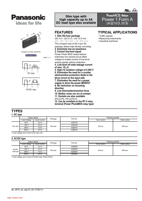
TYPICAL APPLICATIONS
• Traffic signals • Measuring instruments • Industrial machines
Height includes standoff
CAD Data
mm inch
1-Βιβλιοθήκη +23
DC type
-
+
4
1
-
AC/DC type
+
Item LED operate current Input LED turn off current LED dropout voltage On resistance Output Off state leakage current Maximum Maximum Typical Maximum Turn on time* Typical Maximum Transfer characteristics Typical Turn off time* Maximum I/O capacitance Initial I/O isolation resistance Maximum operating speed Vibration resistance Shock resistance Typical Maximum Minimum Maximum Minimum Minimum Ciso Riso — — — Toff 3.0 ms 0.8 pF 1.5 pF 1,000 M 0.5 cps 10 to 55 Hz at double amplitude of 3 mm 4,900 m/s2 {500 G}1 ms 0.22 ms Ton 5.64 ms 5.65 ms 2.57 ms 3.88 ms 10.0 ms 0.21 ms 0.10 ms 0.08 ms ILeak 2.46 ms Typical Maximum Minimum Typical Typical Maximum Typical Ron Symbol IFon IFoff VF 0.11 0.18 AQZ202 AQZ205 AQZ207 1.0 mA 3.0 mA 0.4 mA 0.9 mA 1.25 V (1.16 V at IF = 10 mA) 1.5 V 0.23 0.34 10 A 2.40 ms 1.12 ms 1.65 ms 0.7 1.1 2.1 3.2 AQZ204 IL= 100 mA VL= 10 V IL= 100 mA VL= 10 V IF = 50 mA IF = 10 mA IL =Max. Within 1 s on time IF = 0 mA VL = Max. IF = 10 mA IL = 100 mA VL = 10 V IF = 5 mA IL = 100 mA VL = 10 V IF = 5 mA or 10 mA IL = 100 mA VL = 10 V f = 1 MHz VB = 0 V 500 V DC IF = 10 mA Duty factor = 50% IL = Max., VL = Max. 2 hours for 3 axes 3 times for 3 axes Condition
GBU610;GBU602;GBU608;GBU601;GBU604;中文规格书,Datasheet资料
e 3GBU6005 - GBU6106.0A GLASS PASSIVATED BRIDGE RECTIFIERFeaturesMaximum Ratings and Electrical Characteristics@ T A = 25°C unless otherwise specifiedMechanical DataSingle phase, 60Hz, resistive or inductive load.For capacitive load, derate current by 20%.Notes:1. Unit mounted on 50mm x 50mm x 1.6mm copper plate heatsink.2. Non-repetitive, for t > 1.0ms and < 8.3ms.3. Measured at 1.0MHz and applied reverse voltage of4.0V DC.4.RoHS revision 13.2.2003. Glass and High Temperature Solder Exemptions Applied, see EU Directive Annex Notes 5 and 7.·Case:GBU·Case Material: Molded Plastic. UL Flammability Classification Rating 94V-0·Terminals: Plated Leads.Solderable per MIL-STD-202,Method 208·Lead Free Plating (Tin Finish)·Polarity: Marked on Body·Mounting: Through Hole for #6 Screw ·Mounting Torque: 5.0 Inch-pounds Maximum ·Ordering Information: See Last Page ·Marking: Date Code and Type Number ·Weight: 6.6 grams (approximate)·Glass Passivated Die Construction·High Case Dielectric Strength of 1500VRMS ·Low Reverse Leakage Current ·Surge Overload Rating to 175A Peak ·Ideal for Printed Circuit Board Applications ·UL Listed Under Recognized Component Index, File Number E94661·Lead Free Finish,RoHS Compliant (Note 4)Notes: 5. For packaging details, visit our website at /datasheets/ap02008.pdf0.11.0101000.20.00.61.01.8I ,I N S T A N T A N E O U S F O R W A R D C U R R E N T (A )F V ,INSTANTANEOUS FORWARD VOLTAGE (V)Fig.2Typical Forward Characteristics,per elementF1.44080120160180110100I ,P E A K F O R W A R D S U R G E C U R R E N T (A )F S M NUMBER OF CYCLES AT 60HzFig.3Maximum Non-Repetitive Surge Current00246255075100125150I ,A V E R A G E F O R W A R D R E C T I F I E D C U R R E N T (A )(A V )T ,CASE TEMPERATURE (C)Fig.1Forward Current Derating CurveC °351101001110100C ,T O T A L C A P A C I T A N C E (p F )T V ,REVERSE VOLTAGE (V)Fig.4Typical Total Capacitance,perelementROrdering Information(Note 5)IMPORTANT NOTICEDiodes Incorporated and its subsidiaries reserve the right to make modifications,enhancements,improvements,corrections or other changes without further notice to any product herein.Diodes Incorporated does not assume any liability arising out of the application or use of any product described herein;neither does it convey any license under its patent rights,nor the rights of others.The user of products in such applications shall assume all risks of such use and will agree to hold Diodes Incorporated and all the companies whose products are represented on our website,harmless against all damages.LIFE SUPPORTDiodes Incorporated products are not authorized for use as critical components in life support devices or systems without the expressed written approval of the President of Diodes Incorporated.分销商库存信息:DIODESGBU610GBU602GBU608 GBU601GBU604GBU6005 GBU606。
SIB-110-02-F-S-LC;中文规格书,Datasheet资料
OPTION -LC: LOCKING CLIPS (USE LC-09-TM)(SEE NOTE 13) [N/A WITH THREADED INSERT OPTION -E, -M OR -TI] ROW SPECIFICATION -S: SINGLE (USE SIBM-XX-02-S)
.335 8.509 REF 01
.100 SINGLE INTERFACE BEAM ASSEMBLY
SIB-1XX-XX-XX-S-XX-XX
9/20/2000
SHEET 3 OF 3
/
F:\DWG\MISC\MKTG\SIB-1XX-XX-XX-S-XX-XX-MKT.SLDDRW
BY: DEAN P
FIG. 1
"A"
.150 3.810 REF
.207±.005 5.267±0.127
C3
'A'
.045 1.143 SEE NOTE 11
"A" (No OF POSITIONS -2) x .100[2.54] REF (No OF POSITIONS -1) x .100(2.54) REF
FIG. 2
THREADED INSERT ("C" PLCS)
THREADED INSERT TO BE FLUSH TO BELOW TOP OF BODY
"B" "B" REF "A" REF
SIB-XX-02-S-TI
SECTION "B"-"B"
SIB-120-02-X-S-TI SHOWN
.264 6.706 REF
TIP106G;TIP100G;TIP101G;TIP107G;TIP102;中文规格书,Datasheet资料
50 Units / Rail 50 Units / Rail
50 Units / Rail 50 Units / Rail
50 Units / Rail 50 Units / Rail
50 Units / Rail 50 Units / Rail
RqJA
62.5
°C/W
Stresses exceeding Maximum Ratings may damage the device. Maximum Ratings are stress ratings only. Functional operation above the Recommended Operating Conditions is not implied. Extended exposure to stresses above the Recommended Operating Conditions may affect device reliability. 1. IC = 1.1 A, L = 50 mH, P.R.F. = 10 Hz, VCC = 20 V, RBE = 100 W
TA TC 4.0 80
PD, POWER DISSIPATION (WATTS)
3.0 60
TC 2.0 40
/
1.0 20 TA
00 0
20 40 60 80 100 120 140 160 T, TEMPERATURE (°C)
Figure 2. Power Derating
DARLINGTON 8 AMPERE COMPLEMENTARY SILICON
POWER TRANSISTORS 60−80−100 VOLTS, 80 WATTS
MP2106中文资料
MP21061.5A, 15V, 800KHz Synchronous Buck ConverterThe Future of Analog IC TechnologyTMTMDESCRIPTIONThe MP2106 is a 1.5A, 800KHz synchronous buck converter designed for low voltage applications requiring high efficiency. It is capable of providing output voltages as low as 0.9V, and integrates top and bottom switches to minimize power loss and component count. The 800KHz switching frequency reduces the size of filtering components, further reducing the solution size.The MP2106 includes cycle-by-cycle current limiting and under voltage lockout. The internal power switches, combined with the tiny 10-pin MSOP and QFN packages, provide a solution requiring a minimum of surface area.EVALUATION BOARD REFERENCEBoard Number Dimensions EV2106DQ/DK-00A2.5”X x 2.0”Y x 0.5”ZFEATURES• 1.5A Output Current • Synchronous Rectification • Internal 210m Ω and 255m Ω Power Switches • Input Range of 2.6V to 15V • >90% Efficiency• Zero Current Shutdown Mode • Under Voltage Lockout Protection • Soft-Start Operation • Thermal Shutdown• Internal Current Limit (Source & Sink) • Tiny 10-Pin MSOP or QFN PackageAPPLICATIONS• DC/DC Regulation from Wall Adapters • Portable Entertainment Systems • Set Top Boxes• Digital Video Cameras, DECT • Networking Equipment • Wireless Modems“MPS” and “The Future of Analog IC Technology” are Trademarks of Monolithic Power Systems, Inc.TYPICAL APPLICATION1009080706050403020100E F F I C I E N C Y (%)0.010.1110LOAD CURRENT (A)MP2106_TAC_EC02Efficiency vs.Load CurrentMP2106 – 1.5A, 15V, 800KHz SYNCHRONOUS BUCK CONVERTER TMPACKAGE REFERENCE* For Tape & Reel, add suffix –Z (eg. MP2106DK–Z) For Lead Free, add suffix –LF (eg. MP2106DK–LF–Z)**For Tape & Reel, add suffix –Z (eg. MP2106DQ–Z) For Lead Free, add suffix –LF (eg. MP2106DQ–LF–Z)ABSOLUTE MAXIMUM RATINGS (1) Input Supply Voltage V IN..............................16V LX Voltage V LX.....................–0.3V to V IN + 0.3V BST to LX Voltage.........................–0.3V to +6V Voltage on All Other Pins...............–0.3V to +6V Storage Temperature...............–55°C to +150°C Recommended Operating Conditions (2) Input Supply Voltage V IN..................2.6V to 15V Output Voltage V OUT........................0.9V to 5.5V Operating Temperature..............–40°C to +85°C Thermal Resistance (3) θJA θJC MSOP10................................150.....65...°C/W QFN10....................................50......12...°C/W Notes:1) Exceeding these ratings may damage the device.2) The device is not guaranteed to function outside of itsoperating conditions.3) Measured on approximately 1” square of 1 oz copper.ELECTRICAL CHARACTERISTICSV IN = 5.0V, T A = +25°C, unless otherwise noted.Parameter Symbol ConditionMinTypMaxUnits Input Voltage Range V IN 2.6 15 VInput Under Voltage Lockout 2.2 VInput Under Voltage LockoutHysteresis100 mVShutdown Supply Current V RUN≤ 0.3V 0.5 1.0 µAOperating Supply Current V RUN > 2V, V FB = 1.1V 1.2 1.8 mAVREF Voltage V REF V IN = 2.6V to 15V 2.4 VRUN Input Low Voltage V IL0.4 VRUN Input High Voltage V HL 1.5 VRUNHysteresis 100 mVRUN Input Bias Current 1 µAOscillatorSwitching Frequency f SW700 800 900 KHzMaximum Duty Cycle D MAX V FB = 0.7V 85 %Minimum On Time t ON 200 nsMP2106 – 1.5A, 15V, 800KHz SYNCHRONOUS BUCK CONVERTERTMELECTRICAL CHARACTERISTICS (continued)V IN = 5.0V, T A = +25°C, unless otherwise noted.Parameter Symbol Condition Min Typ Max Units Error Amplifier Voltage Gain A VEA 400 V/V Transconductance G EA 300 µA/V COMP Maximum Output Current ±30 µA FB Regulation Voltage V FB 875 895 915 mV FB Input Bias Current I FB V FB = 0.895V –100 nA Soft-StartSoft-Start Current I SS 2 µA Output Switch On-ResistanceV IN = 5V 255 m ΩSwitch On ResistanceV IN = 3V 315 m Ω V IN = 5V 210 m ΩSynchronous Rectifier On ResistanceV IN = 3V 255 m ΩSwitch Current Limit (Source) 2.5 A Synchronous Rectifier Current Limit(Sink)350 mAThermal Shutdown 160 °CPIN FUNCTIONSPin # Name Description1 SS Soft-Start Input. Place a capacitor from SS to SGND to set the soft-start period. The MP2106sources 2µA from SS to the soft-start capacitor at startup. As the SS voltage rises, thefeedback threshold voltage increases to limit inrush current during startup.2 FBFeedback Input. FB is the inverting input of the internal error amplifier. Connect a resistivevoltage divider from the output voltage to FB to set the output voltage value.3 COMPCompensation Node. COMP is the output of the error amplifier. Connect a series RC networkto compensate the regulation control loop.4 VREFInternal 2.4V Regulator Bypass. Connect a 10nF capacitor between VREF and SGND tobypass the internal regulator. Do not apply any load to VREF.5 RUNOn/Off Control Input. Drive RUN high to turn on the MP2106; low to turn it off. For automaticstartup, connect RUN to VIN via a pullup resistor.6 BSTPower Switch Boost. BST powers the gate of the high-side N-Channel power MOSFET switch.Connect a 10nF or greater capacitor between BST and LX.7 VIN Internal Power Input. VIN supplies the power to the MP2106 through the internal LDOregulator. Bypass VIN to PGND with a 10µF or greater capacitor. Connect VIN to the inputsource voltage.8 LXOutput Switching Node. LX is the source of the high-side N-Channel switch and the drain of thelow-side N-Channel switch. Connect the output LC filter between LX and the output.9 PGNDPower Ground. PGND is the source of the N-Channel MOSFET synchronous rectifier. ConnectPGND to SGND as close to the MP2106 as possible.10 SGND Signal Ground.MP2106 – 1.5A, 15V, 800KHz SYNCHRONOUS BUCK CONVERTERTMTYPICAL PERFORMANCE CHARACTERISTICSCircuit of Figure 2, VIN= 5V, V OUT = 1.8V, L1 = 5µH, C1 = 10µF, C2 = 22µF, T A = +25°C, unless otherwise noted.V OUT1V/div.I L1A/div.MP2106-TPC06Short Circuit ProtectionV OUT1V/div.I L1A/div.Short Circuit RecoveryMP2106-TPC07 V SW5V/div.V OAC Coupled10mV/div.V INAC Coupled200mV/div.I L1A/div.MP2106-TPC01Steady State Operation1.5A LoadV SW5V/div.V OAC Coupled10mV/div.VINAC Coupled20mV/div.I L1A/div.Steady State OperationNo LoadMP2106-TPC02V EN2V/div.V OUT1V/div.V SW5V/div.I L1A/div.1ms/div.MP2106-TPC04Startup from Shutdown1.5A Resistive LoadV EN2V/div.V OUT1V/div.V SW5V/div.I L1A/div.1ms/div.Startup from ShutdownNo LoadMP2106-TPC05V OUTAC Coupled200mV/div.I LOAD1A/div.I L1A/div.MP2106-TPC03Load TransientMP2106 – 1.5A, 15V, 800KHz SYNCHRONOUS BUCK CONVERTERTMOPERATIONMP2106_BD01V OUT Figure 1—Functional Block DiagramMP2106 – 1.5A, 15V, 800KHz SYNCHRONOUS BUCK CONVERTERTMThe MP2106 measures the output voltage through an external resistive voltage divider and compares that voltage to the internal 0.9V reference in order to generate the error voltage at COMP. The current-mode regulator uses the voltage at COMP and compares it to the inductor current to regulate the output voltage. The use of current-mode regulation improves transient response and improves control loop stability.At the beginning of each cycle, the high-side N-Channel MOSFET is turned on, forcing the inductor current to rise. The current at the drain of the high-side MOSFET is internally measured and converted to a voltage by the current sense amplifier.That voltage is compared to the error voltage at COMP. When the inductor current rises sufficiently, the PWM comparator turns off the high-side switch and turns on the low-sideswitch, forcing the inductor current to decrease. The average inductor current is controlled by the voltage at COMP, which in turn is controlled by the output voltage. Thus the output voltage controls the inductor current to satisfy the load. Since the high-side N-Channel MOSFET requires voltages above V IN to drive its gate, a bootstrap capacitor from LX to BST is required to drive the high-side MOSFET gate. When LX is driven low (through the low-side MOSFET), the BST capacitor is internally charged. The voltage at BST is applied to the high-side MOSFET gate to turn it on, and maintains that voltage until the high-side MOSFET is turned off and the low-side MOSFET is turned on, and the cycle repeats. Connect a 10nF or greater capacitor from BST to SW to drive the high-side MOSFET gate.APPLICATION INFORMATIONINPUT 2.6V to 15VC7Figure 2—Typical Application CircuitInternal Low-Dropout RegulatorThe internal power to the MP2106 is supplied from the input voltage (VIN) through an internal 2.4V low-dropout linear regulator, whose output is VREF. Bypass VREF to SGND with a 10nF or greater capacitor for proper operation. The internal regulator can not supply more current than is required to operate the MP2106. Therefore, do not apply any external load to VREF.Soft-StartThe MP2106 includes a soft-start timer that slowly ramps the output voltage at startup to prevent excessive current at the input.When power is applied to the MP2106, and RUN is asserted, a 2µA internal current source charges the external capacitor at SS. As the capacitor charges, the voltage at SS rises. The MP2106 internally limits the feedback threshold voltage at FB to that of the voltage at SS. This forces the output voltage to rise at the same rate as the voltage at SS, forcing the outputMP2106 – 1.5A, 15V, 800KHz SYNCHRONOUS BUCK CONVERTERTMvoltage to ramp linearly from 0V to the desired regulation voltage during soft-start.The soft-start period is determined by the equation:5C 45.0t SS ×=Where C5 (in nF) is the soft-start capacitor fromSS to GND, and t SS (in ms) is the soft-start period. Determine the capacitor required for a given soft-start period by the equation:SS t 22.25C ×=Use values between 10nF and 22nF for C5 to set the soft-start period (between 4ms and 10ms).Setting the Output Voltage (see Figure 2) Set the output voltage by selecting the resistive voltage divider ratio. The voltage divider drops the output voltage to the 0.895V feedback voltage. Use 10k Ω for the low-side resistor of the voltage divider. Determine the high-side resistor by the equation:1R 1V 895.0V 2R OUT×⎟⎟⎠⎞⎜⎜⎝⎛−= Where R2 is the high-side resistor, V OUT is the output voltage and R1 is the low-side resistor. Selecting the Input CapacitorThe input current to the step-down converter is discontinuous, and so a capacitor is required to supply the AC current to the step-down converter while maintaining the DC input voltage. A low ESR capacitor is required to keep the noise at the IC to a minimum. Ceramic capacitors are preferred, but tantalum or low ESR electrolytic capacitors may also suffice. The capacitor can be electrolytic, tantalum or ceramic. Because it absorbs the input switching current it must have an adequate ripple current rating. Use a capacitor with RMS current rating greater than 1/2 of the DC load current.For stable operation, place the input capacitor as close to the IC as possible. A smaller high quality 0.1µF ceramic capacitor may be placed closer to the IC with the larger capacitor placed further away. If using this technique, it is recommended that the larger capacitor be a tantalum or electrolytic type. All ceramiccapacitors should be placed close to the MP2106. For most applications, a 10µF ceramic capacitor will work.Selecting the Output CapacitorThe output capacitor (C2) is required to maintain the DC output voltage. Low ESR capacitors are preferred to keep the output voltage ripple to a minimum. The characteristics of the output capacitor also affect the stability of the regulation control system. Ceramic, tantalum, or low ESR electrolytic capacitors are recommended.The output voltage ripple is:⎟⎟⎠⎞⎜⎜⎝⎛××+×⎟⎟⎠⎞⎜⎜⎝⎛−××=2C f 81R V V 1L f V V SW ESR IN OUT SW OUT RIPPLE Where V RIPPLE is the output voltage ripple, f SW isthe switching frequency, V IN is the input voltage, R ESR is the equivalent series resistance of the output capacitors and f SW is the switching frequency.Choose an output capacitor to satisfy the output ripple requirements of the design. A 22µF ceramic capacitor is suitable for most applications.Selecting the InductorThe inductor is required to supply constant current to the output load while being driven by the switched input voltage. A larger value inductor results in less ripple current that will result in lower output ripple voltage. However, the larger value inductor is likely to have a larger physical size and higher series resistance. Choose an inductor that does not saturate under the worst-case load conditions. A good rule for determining the inductance is to allow the peak-to-peak ripple current to be approximately 30% to 40% of the maximum load current. Make sure that the peak inductor current (the load current plus half the peak-to-peak inductor ripple current) is below 2.5A to prevent loss of regulation due to the current limit.MP2106 – 1.5A, 15V, 800KHz SYNCHRONOUS BUCK CONVERTERTMCalculate the required inductance value by the equation:()If V V V V L SW IN OUT IN OUT ∆××−×=Where ∆I is the peak-to-peak inductor ripple current. It is recommended to choose ∆I to be 30%~40% of the maximum load current.CompensationThe system stability is controlled through the COMP pin. COMP is the output of the internal transconductance error amplifier. A series capacitor-resistor combination sets a pole-zero combination to control the characteristics of the control system. The DC loop gain is:LOAD CS VEA OUTFBVDC R G A VV A ×××⎟⎟⎠⎞⎜⎜⎝⎛= Where V FB is the feedback voltage, A VEA is the transconductance error amplifier voltage gain, G CS is the current sense transconductance (roughly the output current divided by the voltage at COMP) and R LOAD is the load resistance:OUTOUTLOAD I V R =Where I OUT is the output load current.The system has 2 poles of importance, one isdue to the compensation capacitor (C3), and the other is due to the load resistance and the output capacitor (C2), where:3C A 2G f VEA EA1P ××π=P1 is the first pole, and G EA is the error amplifiertransconductance (300µA/V) and2C R 21f LOAD 2P ××π=The system has one zero of importance, due to the compensation capacitor (C3) and the compensation resistor (R3). The zero is:3C 3R 21f 1Z ××π=If large value capacitors with relatively high equivalent-series-resistance (ESR) are used, the zero due to the capacitance and ESR of the output capacitor can be compensated by a third pole set by R3 and C4. The pole is:4C 3R 21f 3P ××π=The system crossover frequency (the frequency where the loop gain drops to 1, or 0dB, is important. Set the crossover frequency to below one tenth of the switching frequency to insure stable operation. Lower crossover frequencies result in slower response and worse transient load recovery. Higher crossover frequencies degrade the phase and/or gain margins and can result in instability.Table 1—Compensation Values for Typical Output Voltage/Capacitor CombinationsV OUTC2 R3 C3 C41.8V 22µF Ceramic 6.8k Ω 3.3nF None2.5V 22µF Ceramic 9.1k Ω 2.2nF None3.3V 22µF Ceramic12k Ω 1.8nF None 1.8V47µF Tantalum (300m Ω)13k Ω 2nF 1nF 2.5V47µF Tantalum (300m Ω)18k Ω 1.2nF 750pF 3.3V47µF Tantalum (300m Ω) 24k Ω 1nF 560pFChoosing the Compensation Components The values of the compensation components given in Table 1 yield a stable control loop for the given output voltage and capacitor. To optimize the compensation components for conditions not listed in Table 1, use the following procedure.MP2106 – 1.5A, 15V, 800KHz SYNCHRONOUS BUCK CONVERTERTMChoose the compensation resistor to set the desired crossover frequency. Determine the value by the following equation:FBCS EA COUT V G G f V 2C 23R ×××××π=Where f C is the desired crossover frequency (preferably 33KHz).Choose the compensation capacitor to set the zero below one fourth of the crossover frequency. Determine the value by the following equation:Cf 3R 23C ××π>Determine if the second compensation capacitor, C4 is required. It is required if the ESR zero of the output capacitor happens at less than half of the switching frequency. Or:1f R 2C SW ESR >×××πIf this is the case, then add the second compensation capacitor.Determine the value by the equation:3R R 2C 4C (max)ESR ×=Where R ESR(MAX) is the maximum ESR of the output capacitor.External Boost DiodeFor input voltages less than or equal to 5V, it is recommended that an external boost diode be added. This will help improve the regulator efficiency. The diode can be a low cost diode such as an IN4148 or BAT54.BOOST DIODE 10nFFigure 3—External Boost DiodeThis diode is also recommended for high duty cycle operation (whenINOUTV V >65%) and high output voltage (V OUT >12V) applications. However, do not exceed the absolute maximum voltage for these pins.MP2106 – 1.5A, 15V, 800KHz SYNCHRONOUS BUCK CONVERTERTMPACKAGE INFORMATIONMSOP10MP2106 – 1.5A, 15V, 800KHz SYNCHRONOUS BUCK CONVERTERNOTICE: The information in this document is subject to change without notice. Please contact MPS for current specifications. Users should warrant and guarantee that third party Intellectual Property rights are not infringed upon when integrating MPS products into any application. MPS will not assume any legal responsibility for any said applications.MP2106 Rev. 1.6 11 2/22/2006MPS Proprietary Information. Unauthorized Photocopy and Duplication Prohibited. © 2006 MPS. All Rights Reserved. TM QFN10 (3mm x 3mm)元器件交易网。
- 1、下载文档前请自行甄别文档内容的完整性,平台不提供额外的编辑、内容补充、找答案等附加服务。
- 2、"仅部分预览"的文档,不可在线预览部分如存在完整性等问题,可反馈申请退款(可完整预览的文档不适用该条件!)。
- 3、如文档侵犯您的权益,请联系客服反馈,我们会尽快为您处理(人工客服工作时间:9:00-18:30)。
SPEC NO: DSAH0046 REV NO: V.5 DATE: OCT/09/2010 PAGE: 1 OF 5
APPROVED: WYNEC CHECKED: Allen Liu DRAWN: C.H.Han ERP: 1203000509
2.1x0.6mm RIGHT ANGLE SURFACE LED
LAMP
ATTENTION
OBSERVE PRECAUTIONS
FOR HANDLING
ELECTROSTATIC
DISCHARGE
SENSITIVE
DEVICES
Part Number: APA2106QBC/D Blue
Features z2.1mmX0.6mm right angle SMT LED, 1.0mm thickness. zLow power consumption. zWide viewing angle. zIdeal for backlight and indicator. zVarious colors and lens types available. zPackage: 2000pcs / reel. zMoisture sensitivity level : level 3. zRoHS compliant. Description
The Blue source color devices are made with InGaN Light
Emitting Diode.
Static electricity and surge damage the LEDS.
It is recommended to use a wrist band or anti-electrostatic
glove when handling the LEDs.
All devices, equipment and machinery must be electrically
grounded.
Package Dimensions
Notes:
1. All dimensions are in millimeters (inches).
2.Tolerance is ±0.1(0.004") unless otherwise noted.
3.The specifications, characteristics and technical data described in the datasheet are subject to change without prior notice.
4. The device has a single mounting surface. The device must be mounted according to the specifications
芯天下--http://oneic.com/
SPEC NO: DSAH0046 REV NO: V.5 DATE: OCT/09/2010 PAGE: 2 OF 5
APPROVED: WYNEC CHECKED: Allen Liu DRAWN: C.H.Han ERP: 1203000509
Selection Guide
Notes:
1. θ1/2 is the angle from optical centerline where the luminous intensity is 1/2 of the optical peak value.
2. Luminous intensity/ luminous Flux: +/-15%.
Absolute Maximum Ratings at TA=25°C
Electrical / Optical Characteristics at TA=25°C
Notes:
1.Wavelength: +/-1nm.
2. Forward Voltage: +/-0.1V.
Note:
1. 1/10 Duty Cycle, 0.1ms Pulse Width.
Part No. Dice Lens Type
Viewing Angle [1] Min. Typ. 2θ1/2 APA2106QBC/D Blue (InGaN) Water Clear 45 80 120° Iv (mcd) [2]
@ 20mA
Symbol Parameter Device Typ. Max. Units Test Conditions
λpeak Peak Wavelength Blue 468 nm IF=20mA
λD [1] Dominant Wavelength Blue 470 nm I
F
=20mA
Δλ1/2 Spectral Line Half-width Blue 25 nm I
F
=20mA
C Capacitance Blue 100 pF VF=0V;f=1MHz
V
F [2] Forward Voltage Blue 3.3 4 V IF
=20mA
IR Reverse Current Blue 50 uA VR=5V
Parameter Blue Units
Power dissipation 120 mW
DC Forward Current 30 mA
Peak Forward Current [1] 150 mA
Reverse Voltage 5 V
Operating Temperature -40°C To +85°C
Storage Temperature -40°C To +85°C
芯天下--http://oneic.com/
SPEC NO: DSAH0046 REV NO: V.5 DATE: OCT/09/2010 PAGE: 3 OF 5
APPROVED: WYNEC CHECKED: Allen Liu DRAWN: C.H.Han ERP: 1203000509
Blue APA2106QBC/D
芯天下--http://oneic.com/
SPEC NO: DSAH0046 REV NO: V.5 DATE: OCT/09/2010 PAGE: 4 OF 5
APPROVED: WYNEC CHECKED: Allen Liu DRAWN: C.H.Han ERP: 1203000509
APA2106QBC/D
Reflow soldering is recommended and the soldering profile is shown below.
Other soldering methods are not recommended as they might cause damage to the product.
Recommended Soldering Pattern (Units : mm; Tolerance: ± 0.1) Reel Dimension
Tape Dimensions
(Units : mm)
芯天下--http://oneic.com/
SPEC NO: DSAH0046 REV NO: V.5 DATE: OCT/09/2010 PAGE: 5 OF 5
APPROVED: WYNEC CHECKED: Allen Liu DRAWN: C.H.Han ERP: 1203000509
PACKING & LABEL SPECIFICATIONS APA2106QBC/D
芯天下--http://oneic.com/