Flash存储器概述
This document contains information on one or more products under development at Spansion LLC. The information is intended to help you evaluate this product. Do not design in this product without contacting the factory. Spansion LLC reserves the right to change or discontinue work on this proposed product without notice.
Publication Number FlashOverview_AN Revision A Amendment 0 Issue Date November 10, 2005
Introduction
All computer-based systems contain memory. Memory is where information is stored while waiting to be operated on by the Central Processing Unit (CPU) of the computer . There are two types of memory. They are volatile memory and non-volatile memory. Volatile memory retains its information only while power is applied to the memory de-vice. The contents of this memory type may be easily and quickly changed. Non-volatile memory retains its information even when no power is applied to the memory device. Although the information in most non-volatile memories may be changed, the process involved is much slower than for volatile memory.
Volatile Memory
Volatile memory loses its contents when the device loses power . Random Access Mem-ory (RAM) is the traditional name used for volatile memory. The name refers to the ability to access any location of the memory quickly with no particular order of accesses needed. Static RAM (SRAM) and Dynamic RAM (DRAM) are two examples of volatile memories that have this characteristic.
SRAM typically uses six transistors for each memory bit (cell) to retain data as long as power is being supplied. This makes each memory cell relatively large and limits SRAM to use in lower density memories. SRAM can provide faster access to data, use less standby power , and tends to be more expensive than DRAM.
DRAM uses a single transistor and a small capacitor for each bit of memory. Since ca-pacitors do not hold a charge indefinitely, DRAM cells must be frequently recharged (refreshed) to avoid losing the contents. These smaller memory cells allow DRAM to be used for high density, low cost memories, but are typically slower than SRAM.
Flash Memory: An Overview
Application Note
Non-Volatile Memory
Non-volatile memory is memory that retains its contents even if the power is lost. Non-
volatile memory was originally called Read Only Memory (ROM) because its contents
were loaded during the manufacturing process and could be read, but never erased or
reprogrammed. Over time, the ability to erase and reprogram ROM was added in differ-
ent ways and referred to as Electrically Programmable ROM (EPROM), Electrically
Erasable and Programmable ROM (EEPROM), and Flash EEPROM - commonly referred
to simply as Flash memory.
ROM memory is programmed by the way it is manufactured and stores permanent code
and data that is generally used to initialize and operate a computer system.
EPROM can be electrically programmed one byte at a time but is not electrically eras-
able. It has to be exposed to ultra-violet (UV) light for about twenty minutes in order to
erase all bits in the memory array. EPROM uses a single transistor for each data bit and
can be used in relatively high density memories.
EEPROM is electrically erasable and programmable in-system, one byte at a time, but
the memory cells use more transistors and are larger than those in EPROMs, thus
EEPROM has higher costs and lower density (generally less than 1 Mb).
Flash EEPROM memory can be electrically programmed a single byte or word at a
time, but a large group of bytes or words - called a block, sector, or page - are electri-
cally erased at the same time. Due to the erase operation being much faster than the
prior EPROM or EEPROM devices, these devices came to be called Flash erase EEPROM,
or simply Flash memories. The Flash memory cell uses a single transistor to store one
or more bits of information. Flash technology combines the high density of EPROM with
the electrical in-system erase and programmability of EEPROMs. Flash memory has be-
come the dominant type of non-volatile memory in use.
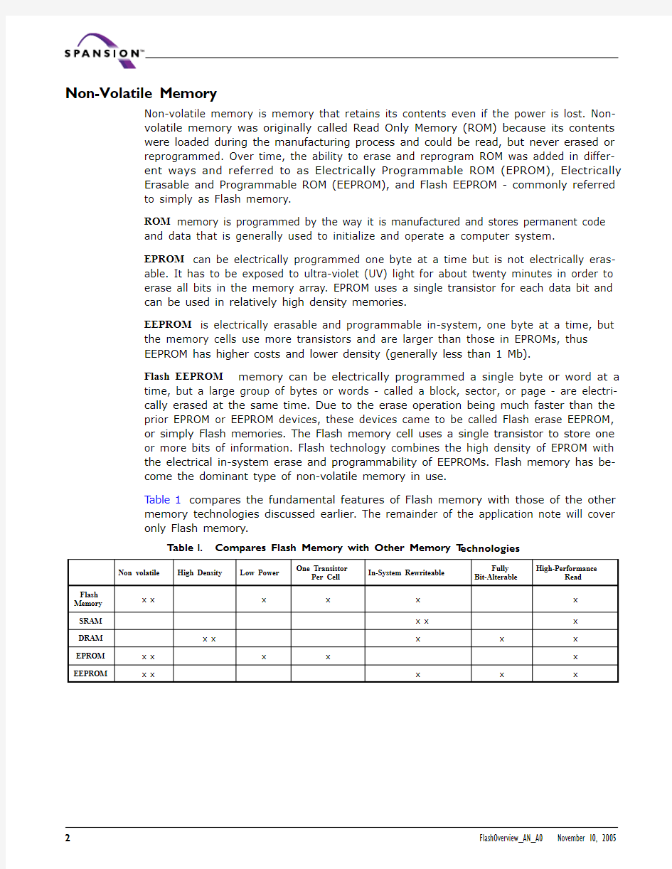
Table 1 compares the fundamental features of Flash memory with those of the other
memory technologies discussed earlier. The remainder of the application note will cover
only Flash memory.
T able 1. Compares Flash Memory with Other Memory T echnologies
Non volatile High Density Low Power One Transistor
Per Cell In-System Rewriteable
Fully
Bit-Alterable
High-Performance
Read
Flash
Memory x x x x x x
SRAM x x
x DRAM x x
x
x
x EPROM x x x x x
EEPROM x x x
x
x
2FlashOverview_AN_A0 November 10, 2005
Flash Memory Architectures
The two main architectures dominate the Flash memory: they are NOR and NAND.
NOR is typically used for code storage and execution. NOR allows quick random access
to any location in the memory array, 100% known good bits for the life of the part, and
code execution directly from NOR Flash memory.
NAND is used for data storage. NAND Flash requires a relatively long initial read access
to the memory array, 98% good bits when shipped with additional bit failure over the
life of the part (ECC highly recommended), program/erase times are much faster than
NOR and NAND cost less per bit than NOR.
T able 2. Difference Between NOR and NAND
Parameter NOR NAND
Density 1Mbit – 1Gbit 64Mbit - 16Gbit
Read initial access 55ns 10,000ns
Read sequential access 9ns 50ns
Program 0.3 Mbytes / s 2.6 Mbytes / s
Erase 0.2 Mbytes / s 8.2 Mbytes / s
Access Method Random Sequential
Spansion Flash Memory
Spansion is the world's leading supplier of NOR Flash memory. Spansion Flash memory
products include a broad spectrum of densities and features to support a wide range of
customer specific markets such as hand-held/mobile electronics, computer, set-top
boxes and automotive applications. Spansion primarily uses two Flash memory technol-
ogies, Floating Gate and MirrorBit.
Floating Gate technology was first introduced in the early 1990's. It offered fast access
times, and high program/erase endurance cycles. This technology allowed the storage
of only one data bit per cell. However, with the introduction of MirrorBit technology in
2001, Spansion is able to offer a more cost-effective solution to customers, while still
maintaining fast access times and high endurance cycles. The cost effective solution is
the design of the MirrorBit storage cell, which can store two data bits per cell, instead
of just one data bit. This design enables manufacturing costs to be significantly lower
than that of Floating Gate technology. MirrorBit technology definitely has a clear eco-
nomical, as well as a technological advantage over Floating Gate technology. November 10, 2005 FlashOverview_AN_A03
Distinctive Features
Spansion Flash memory offers many distinctive features that help designers build fea-
ture-rich, cost-effective systems. Key distinctive characteristics include:
Secured Silicon (SecSi) Sector
ACC
WP#
VI/O
CFI
Write Buffer
Advanced Sector Protection
Page Mode
Burst Mode
Simultaneous Read/Write
SecSi (Secured Silicon) feature enables permanent part identification through an Elec-
tronic Serial Number (ESN). The SecSi sector provides a 128 Bytes to 64 Kbytes area
for code or data that can be permanently protected. Once this sector is protected, no
further changes within the sector can occur. SecSi Sector Indicator Bit (DQ7) is used to
determine whether or not the SecSi sector is protected. The Spansion offers the device
with the SecSi sector either customer lockable or factory locked. The customer-lockable
version is shipped with the SecSi sector unprotected and has the SecSi Sector Indicator
Bit permanently set to a "0". The factory- locked version is always protected and has
the SecSi Sector Indicator Bit permanently set to a "1".
ACC (Accelerated Program Operation) is an input pin which allows for faster program-
ming or erases operation when raised to a specified voltage (12v or 9v).
WP# (Write Protect) is a hardware method for protecting boot sectors using standard
control logic signals.
V I/O is a feature that allows the signal interface voltage levels to be determined by the
V I/O power supply.
CFI is a feature which provides device-specific information to the system, allowing host
software to easily reconfigure for different Flash devices. The device enters the CFI
Query mode when the system writes the CFI Query command, 98h, to address 55h, any
time the device is ready to read array data. The system can also write the CFI Query
command when the device is in the Autoselect mode.
Write Buffer allows the system to write up to 32 words in one programming operation.
It is implemented to speed up programming operations. A Write Buffer is a set of reg-
isters used to hold several words that are to be programmed as a group.
Advanced Sector Protection provides command-controlled rather than voltage-con-
trolled protection to any sector against inadvertent or malicious program or erase
operations. Refer to the datasheet for detailed information.
Page Mode allows high speed random read access to memory addresses near the initial
access address.
Burst Mode allows high speed sequential reading of the Flash without the need to up-
date the address lines.
4FlashOverview_AN_A0 November 10, 2005
November 10, 2005 FlashOverview_AN_A05
Simultaneous Read/Write allows the flash to be read from at the same time a pro-gram or erase operation is being performed.
Basic Operation
There are three basic operations in a Flash memory: read (a byte or a word), program (a byte or a word), and erase (one or more sectors).
Read
Spansion provides three types of read operations: asynchronous read, asynchronous page read and synchronous burst read. Asynchronous read is a read not occurring at predetermined or regular intervals (not dependent on a clock). Typical read access time is 55 to 120ns. Figure 1 shows the timing diagram.
Figure 1. Asynchronous Read Operation Timing
Asynchronous page read is an asynchronous read operation of several words, in which the first word of the group takes a longer initial access time, and subsequent words in the group take less “page” access time to be read. The page size of the page mode de-vices is either 4 words or 8 words, with the page being selected by the least significant two or three bits of address. Page mode interface provides faster read access speed for random locations within a page. Initial access time is typically 70 to 120ns. Access time within a page is typically 25ns. Figure 2
shows the page read timing diagram.
Figure 2. Page Read Timing
Synchronous burst read is a read occurring at regular intervals dependent on a clock
edge. Burst mode devices require three extra control pins to perform burst read. They
are Clock, Load Burst Address (LBA#) or Address Valid (ADV#), and Burst Address Ad-
vance (BAA#) or RDY.
When the burst device first powers up, it is enabled for asynchronous read operation.
To enable synchronous burst read, the system must issue the burst mode enable com-
mand sequence. The initial address of an access is loaded by the clock edge when LBA#
or AVD# is low. The first data word is available after the initial access time delay. Se-
quential words are available on each following clock edge after the burst access time
delay. Typical initial access time is 50 to 70ns. Burst accesses can continue with a 50-
to 80-MHz clock.
Depending on the specific device, Spansion burst mode flash offers a number of read
modes to interface with a wide range of microprocessors. They are linear burst, inter-
leaved burst, and continuous sequential burst. In the linear and interleaved burst
modes, the device delivers a stream of words from a 4, 8, 16, or 32 word aligned block.
(For the S29CD family, the burst is 32-bit double words.) If the initial address is not at
the beginning of the block, the sequence of words following the initial access will wrap
from the end to the beginning of the block. In continuous sequential burst mode the
device reads sequentially through the entire address range. Refer to a specific burst de-
vice datasheet for detailed information. Figure 3 shows burst read mode.
6FlashOverview_AN_A0 November 10, 2005
Figure 3. Burst Read Timing
Program
The unprogrammed state of a Flash memory cell is a high signal level or logical one. Chang-
ing a flash memory cell (or bit) to a low voltage level or zero is called programming.
Programming on Spansion Floating Gate Flash is generally done one byte or word at a time.
MirrorBit technology uses a write buffer to program one byte to as many as 32 bytes.
One key point to note is that programming only changes ones to zeros. Programming is ini-
tiated by a series of write accesses that form a program command. The required sequence
of write accesses prevents unintended changes to stored data.
Erase
Erasure of a Flash device is done through multiple write accesses that form an erase com-
mand. The erase completion time is dependent upon the sector size and technology. The
erase command sequence initiates the embedded erase algorithm - an internal algorithm
that automatically preprograms the memory array (if it is not already programmed) before
executing the erase operation simultaneously on all bits of the sector.
One key point to note is that chip or sector erasing only changes zeros to ones. During erase,
the device automatically times the erase pulse widths and verifies the proper cell margin. T emperature Ranges
Spansion Flash memory devices are available in various temperature ranges.
T able 3. Various T emperature Options
Code Name Description
C Commercial 0 - +70oC
W Wireless -25 - +85oC
I Industrial -40 - +85oC
cabin -40-
+105oC
V Automotive-In
N Extended -40 - +125oC
H Hot -40 - +145oC
November 10, 2005 FlashOverview_AN_A07
8FlashOverview_AN_A0 November 10, 2005
Spansion Product Families
Note: Devices have prefixes such as Am29, S29, and MBM29.
Conclusion
Spansion Flash memory provides a compact, easy to use, non-volatile code and data storage solution for electronic products. Spansion provides a broad portfolio of Flash memories to suit a wide range of applications. The memory size, voltage, speed, and package, can be selected to suit the application.
T able 4. AMD/Fujitsu Legacy Product Families
Product Family
Architecture
Density Voltage SL Super Low-Voltage Standard Flash Memory
4Mb – 16 Mb 1.8V LV Low-Voltage Standard Flash Memory
1Mb – 128Mb 3.0V F Standard Flash Memory 1Mb – 32Mb 5.0V DL Simultaneous Read/Write, Low Voltage Flash Memory 4Mb – 128Mb 3.0V BL High Performance Burst Mode Flash Memory
8Mb and 16Mb 3.0V PL High Performance Page Mode Flash Memory
16Mb and 32Mb 3.0V DS Simultaneous Read/Write, Super Low Voltage Flash Memory 16Mb and 32Mb 1.8V BDS Burst, Simultaneous Read/Write, Super Low Voltage Flash Memory 32Mb – 128Mb
1.8V
BDD Burst, Simultaneous Read/Write Flash Memory
16Mb 2.5V LV-M MirrorBit? Technology, Low Voltage Flash Memory
1Mb – 256Mb
3.0V
PDS Page, Simultaneous Read/Write, Super Low Voltage Flash Memory 32Mb 1.8V PDL Page, Simultaneous Read/Write, Low Voltage Flash Memory 64Mb and 128Mb 3.0V AL Low Voltage Standard Flash Memory
4Mb - 32Mb 3.0V CD 32-bit, Burst, Simultaneous Read/Write Flash Memory 16Mb – 32Mb 2.5V GL MirrorBit? Technology, Page Mode Flash Memory
16Mb – 512Mb 3.0V PL Simultaneous Read/Write, Page Mode Flash Memory
32Mb – 256Mb 3.0V WS Simultaneous Read/Write, Burst Mode Flash Memory
64Mb – 256Mb 1.8V JL
Simultaneous Read/Write Flash Memory
32Mb - 64Mb
3.0V
Revision History
Revision A0 (November 10, 2005)
Initial Release.
Colophon
The products described in this document are designed, developed and manufactured as contemplated for general use, including without limitation, ordinary industrial use, general office use, personal use, and household use, but are not designed, developed and manufactured as contemplated (1) for any use that includes fatal risks or dangers that, unless extremely high safety is secured, could have a serious effect to the public, and could lead directly to death, personal injury, severe physical damage or other loss (i.e., nuclear reaction control in nuclear facility, aircraft flight control, air traffic control, mass transport control, medical life support system, missile launch control in weapon system), or (2) for any use where chance of failure is intolerable (i.e., submersible repeater and artificial satellite). Please note that Spansion LLC will not be liable to you and/or any third party for any claims or damages arising in connection with above-mentioned uses of the products. Any semiconductor devices have an inherent chance of failure. Y ou must protect against injury, damage or loss from such failures by incorporating safety design measures into your facility and equipment such as redundancy, fire protection, and prevention of over-current levels and other abnormal operating conditions. If any products described in this document represent goods or technologies subject to certain restrictions on ex-port under the Foreign Exchange and Foreign T rade Law of Japan, the US Export Administration Regulations or the applicable laws of any other country, the prior authorization by the respective government entity will be required for export of those products.
Trademarks and Notice
The contents of this document are subject to change without notice. This document may contain information on a Spansion LLC product under development by Spansion LLC. Spansion LLC reserves the right to change or discontinue work on any product without notice. The information in this document is provided as is without warranty or guarantee of any kind as to its accuracy, completeness, operability, fitness for particular purpose, merchantability, non-infringement of third-party rights, or any other warranty, express, implied, or statutory. Spansion LLC assumes no liability for any damages of any kind arising out of the use of the information in this document.
Copyright ?2004 – 2005 Spansion LLC. All rights reserved. Spansion, the Spansion logo, and MirrorBit are trademarks of Spansion LLC. Other company and product names used in this publication are for identification purposes only and may be trademarks of their respective companies.
November 10, 2005 FlashOverview_AN_A09
第13章 Flash存储器
第13章Flash存储器 Flash存储器具有电可擦除、无需后备电源来保护数据、可在线编程、存储密度高、低功耗、成本较低等特点,这使得Flash存储器在嵌入式系统中的使用迅速增长。 本章主要以HC08系列中的GP32为例阐述Flash存储器的在线编程方法,也简要阐述了HCS08系列中GB60的在线编程方法。本章首先概述了Flash存储器的基本特点,并介绍其编程模式,随后给出M68HC908GP32的Flash存储器编程的基本操作及汇编语言和C语言的在线编程实例。最后讨论MC9S08GB60的Flash存储器编程方法。 Flash存储器编程方法有写入器模式与在线模式两种,本章讨论的是在线模式。有的芯片内部ROM中,包含了Flash擦除与写入子程序,在本章的进一步讨论中给出了调用方法,使Flash编程相对方便。有的芯片内部ROM中没有固化Flash擦除与写入子程序,只能自己编写Flash擦除与写入子程序。而编写Flash擦除与写入子程序需要较严格的规范,所以这是比较细致的工作,读者应仔细分析本章的例程,并参照例程编程。掌握了GP32芯片的Flash编程方法后,可以把此方法应用于整个系列的Flash编程。Flash在线编程对初学者有一定难度,希望通过实例分析学习。本章给出Flash在线编程的C语言实例,对于训练C语言与汇编联合编程技巧很有帮助。 13.1 Flash存储器概述与编程模式 理想的存储器应该具备存取速度快、不易失、存储密度高(单位体积存储容量大)、价格低等特点,但一般的存储器只具有这些特点中的一个或几个。近几年Flash存储器(有的译为:闪速存储器或快擦型存储器)技术趋于成熟,它结合了OTP存储器的成本优势和EEPROM的可再编程性能,是目前比较理想的存储器。Flash存储器具有电可擦除、无需后备电源来保护数据、可在线编程、存储密度高、低功耗、成本较低等特点。这些特点使得Flash存储器在嵌入式系统中获得广泛使用。从软件角度来看,Flash和EEPROM技术十分相似,主要的差别是Flash存储器一次只能擦除一个扇区,而不是EEPROM存储器的1个字节1个字节地擦除,典型的扇区大小是128B~16KB。尽管如此,因为Flash存储器的总体性价比,它还是比EEPROM更加流行,并且迅速取代了很多ROM器件。 嵌入式系统中使用Flash存储器有两种形式:一种是嵌入式处理器上集成了Flash,另一种是片外扩展Flash。 目前,许多MCU内部都集成了Flash存储器。Freescale公司在Flash存储器技术相当成熟的时候,在HC08系列单片机内集成了Flash存储器。该系列内部的Flash存储器不但可用编程器对其编程,而且可以由内部程序在线写入(编程),给嵌入式系统设计与编程提供了方便。存储器是MCU的重要组成部分,存储器技术的发展对MCU的发展起到了极大的推动作用。对于Freescale公司新推出的HCS08系列MCU采用第三
flash存储原理.
flash存储原理 一、半导体存储设备的原理 目前市面上出现了大量的便携式存储设备,这些设备大部分是以半导体芯片为存储介质的。采用半导体存储介质,可以把体积变的很小,便于携带;与硬盘之类的存储设备不同,它没有机械结构,所以也不怕碰撞;没有机械噪声;与其它存储设备相比,耗电量很小;读写速度也非常快。半导体存储设备的主要缺点就是价格和容量。 现在的半导体存储设备普遍采用了一种叫做“FLASH MEMORY”的技术。从字面上可理解为闪速存储器,它的擦写速度快是相对于EPROM而言的。FLASH MEMORY是一种非易失型存储器,因为掉电后,芯片内的数据不会丢失,所以很适合用来作电脑的外部存储设备。它采用电擦写方式、可10万次重复擦写、擦写速度快、耗电量小。 1.NOR型FLASH芯片 我们知道三极管具备导通和不导通两种状态,这两种状态可以用来表示数据0和数据1,因此利用三极管作为存储单元的三极管阵列就可作为存储设备。FLASH 技术是采用特殊的浮栅场效应管作为存储单元。这种场效应管的结构与普通场管有很大区别。它具有两个栅极,一个如普通场管栅极一样,用导线引出,称为“选择栅”;另一个则处于二氧化硅的包围之中不与任何部分相连,这个不与任何部分相连的栅极称为“浮栅”。通常情况下,浮栅不带电荷,则场效应管处于不导通状态,场效应管的漏极电平为高,则表示数据1。编程时,场效应管的漏极和选择栅都加上较高的编程电压,源极则接地。这样大量电子从源极流向漏极,形成相当大的电流,产生大量热电子,并从衬底的二氧化硅层俘获电子,由于电子的密度大,有的电子就到达了衬底与浮栅之间的二氧化硅层,这时由于选择栅加有高电压,在电场作用下,这些电子又通过二氧化硅层到达浮栅,并在浮栅上形成电子团。浮栅上的电子团即使在掉电的情况下,仍然会存留在浮栅上,所以信息能够长期保存(通常来说,这个时间可达10年。由于浮栅为负,所以选择栅为正,在存储器电路中,源极接地,所以相当于场效应管导通,漏极电平为低,即数据0被写入。擦除时,源极加上较高的编程电压,选择栅接地,漏极开
Flash存储器的技术和发展
湘潭大学论文 题目:关于Flash存储器的技术和发展 学院:材料与光电物理学院 专业:微电子学 学号:2010700518 姓名:李翼缚 完成日期:2014.2.24
目录 1引言 (4) 2Flash 存储器的基本工作原理 (4) 3 Flash存储器的编程机制 (5) 3.1 沟道热电子注入(CHE) (5) 3.2 F-N隧穿效应(F-NTunneling) (6) 4 Flash存储器的单元结构 (6) 5 Flash存储器的可靠性 (7) 5.1 CHE编程条件下的可靠性机制 (8) 5.2 隧道氧化层高场应力下的可靠性机制 (8) 6 Flash存储器的发展现状和未来趋势 (9) 参考文献: (10)
关于Flash存储器的技术和发展 摘要:Flash 存储器是在20世纪80年代末逐渐发展起来的一种新型半导体不挥发性存储器,它具有结构简单、高密度、低成本、高可靠性和在系统的电可擦除性等优点, 是当今半导体存储器市场中发展最为迅速的一种存储器。文章对F lash 存储器的发展历史和工作机理、单元结构与阵列结构、可靠性、世界发展的现状和未来趋势等进行了深入的探讨。 关键词:半导体存储器;不挥发性存储器; Flash存储器; ETOX结构 About Flash Memory Technology and Its Development Abstract: As a new non -volatile semiconductor memory introduced by Masuoka in 1984, flash memory has a number of advantages, such as simple structure, high integration density, low cost, and high reliability, and it is widely used in mobile phone, digital camer a, PCBIOS, DVD player, and soon. Its evolution, programming mechanism, cell structure, array structure, reliability are described, and its developing trend in the future is dis cussed. Key words: Semico nduct or memory; Flash memor y; Non-volatile memory ; ETOX
Flash做为存储器存储数据
STM32学习笔记-Flash做为存储器储存数据 说到STM32的FLSAH,我们的第一反应是用来装程序的,实际上,STM32的片内FLASH不仅用来装程序,还用来装芯片配置、芯片ID、自举程序等等。当然, FLASH 还可以用来装数据。 自己收集了一些资料,现将这些资料总结了一下,不想看的可以直接调到后面看怎么操作就可以了。 FLASH分类 根据用途,STM32片内的FLASH分成两部分:主存储块、信息块。主存储块用于存储程序,我们写的程序一般存储在这里。信息块又分成两部分:系统存储器、选项字节。系统存储器存储用于存放在系统存储器自举模式下的启动程序(BootLoader),当使用ISP方式加载程序时,就是由这个程序执行。这个区域由芯片厂写入BootLoader,然后锁死,用户是无法改变这个区域的。选项字节存储芯片的配置信息及对主存储块的保护信息。 FLASH的页面 STM32的FLASH主存储块按页组织,有的产品每页1KB,有的产品每页2KB。页面典型的用途就是用于按页擦除FLASH。从这点来看,页面有点像通用FLASH 的扇区。 STM32产品的分类 STM32根据FLASH主存储块容量、页面的不同,系统存储器的不同,分为小容量、中容量、大容量、互联型,共四类产品。 小容量产品主存储块1-32KB,每页1KB。系统存储器2KB。 中容量产品主存储块64-128KB,每页1KB。系统存储器2KB。 大容量产品主存储块256KB以上,每页2KB。系统存储器2KB。 互联型产品主存储块256KB以上,每页2KB。系统存储器18KB。 对于具体一个产品属于哪类,可以查数据手册,或根据以下简单的规则进行区分: STM32F101xx、STM32F102xx 、STM32F103xx产品,根据其主存储块容量,一定是小容量、中容量、大容量产品中的一种,STM32F105xx、STM32F107xx是互联型产品。 互联型产品与其它三类的不同之处就是BootLoader的不同,小中大容量产品的BootLoader只有2KB,只能通过USART1进行ISP,而互联型产品的BootLoader有18KB,能通过USAT1、4、CAN等多种方式进行ISP。小空量产品、中容量产品的BootLoader与大容量产品相同。 关于ISP与IAP ISP(In System Programming)在系统编程,是指直接在目标电路板上对芯片进行编程,一般需要一个自举程序(BootLoader)来执行。ISP也有叫ICP (In Circuit Programming)、在电路编程、在线编程。 IAP(In Application Programming)在应用中编程,是指最终产品出厂后,由最终用户在使用中对用
嵌入式—flash存储器
存储器存储器 FLASH存储器存储器章FLASH 13章 第13
本章主要内容 Flash Flash存储器概述与编程模式存储器概述与编程模式存储器 MC908GP32MC908GP32单片机单片机单片机Flash Flash Flash存储器编程方法存储器编程方法存储器GP32GP32单片机单片机单片机Flash Flash Flash在线编程汇编语言实例在线编程汇编语言实例GP32GP32单片机单片机单片机Flash Flash Flash在线编程在线编程在线编程08C 08C 08C语言实例语言实例HCS08HCS08系列单片机系列单片机系列单片机Flash Flash Flash编程方法编程方法
13.1 Flash 13.1 Flash存储器概述与编程模式存储器概述与编程模式13.1.1 Flash存储器的基本特点与编程模式 (1) Flash存储器的基本特点 ①固有不挥发性::Flash Flash存储器不需要后备电源来保持数据存储器不需要后备电源来保持数据存储器不需要后备电源来保持数据。。所以所以,,它具有磁存储器无需电能保持数据的优点它具有磁存储器无需电能保持数据的优点。。 ②易更新性易更新性:Flash :Flash :Flash存储器具有电可擦除特点存储器具有电可擦除特点存储器具有电可擦除特点。。相对于相对于EPROM(EPROM(EPROM(电可编电可编程只读存储器程只读存储器))的紫外线擦除工艺的紫外线擦除工艺,,Flash Flash存储器的电擦除功能为开发者存储器的电擦除功能为开发者节省了时间节省了时间,,也为最终用户更新存储器内容提供了可能也为最终用户更新存储器内容提供了可能。。 ③成本低成本低、、密度高密度高、、可靠性好可靠性好::与EEPROM(EEPROM(电可擦除可编程的只读存电可擦除可编程的只读存储器储器))相比较相比较,,Flash Flash存储器的成本更低存储器的成本更低存储器的成本更低、、密度更高密度更高、、可靠性更好可靠性更好。。
FLASH闪存总体介绍
Flash闪存器总体介绍 闪存的英文名称是“Flash Memory”,一般简称为“Flash”,它属于内存器件的一种。 不过闪存的物理特性与常见的内存有根本性的差异: 目前各类DDR、SDRAM或者RDRAM都属于挥发性内存,只要停止电流供应内存中的数据便无法保持,因此每次电脑开机都需要把数据重新载入内存; 闪存则是一种不挥发性(Non-V olatile)内存,在没有电流供应的条件下也能够长久地保持数据,其存储特性相当于硬盘,这项特性正是闪存得以成为各类便携型数字设备的存储介质的基础。 NAND闪存的存储单元则采用串行结构,存储单元的读写是以页和块为单位来进行(一页包含若干字节,若干页则组成储存块,NAND的存储块大小为8到32KB),这种结构最大的优点在于容量可以做得很大,超过512MB容量的NAND 产品相当普遍,NAND 闪存的成本较低,有利于大规模普及。 NAND闪存的缺点在于读速度较慢,它的I/O 端口只有8个,比 NOR 要少多了。这区区8个I/O 端口只能以信号轮流传送的方式完成数据的传送,速度要比NOR闪存的并行传输模式慢得多。再加NAND闪存的逻辑为电子盘模
块结构,内部不存在专门的存储控制器,一旦出现数据坏块将无法修,可靠性较NOR 闪存要差。 NAND闪存被广泛用于移动存储、数码相机、MP3播放器、掌上电脑等新兴数字设备中。由于受到数码设备强劲发展的带动, NAND 闪存一直呈现指数级的超高速增长. NOR和NAND是现在市场上两种主要的非易失闪存技术。Intel于1988年首先开发出NOR flash技术,彻底改变了原先由EPROM和EEPROM一统天下的局面。紧接着,1989年,东芝公司发表了NAND flash结构,强调降低每比特的成本,更高的性能,并且象磁盘一样可以通过接口轻松升级。但是经过了十多年之后,仍然有相当多的硬件工程师分不清NOR和NAND闪存。 相“flash存储器”经常可以与相“NOR存储器”互换使用。许多业内人士也搞不清楚NAND闪存技术相对于NOR技术的优越之处,因为大多数情况下闪存只是用来存储少量的代码,这时NOR闪存更适合一些。而NAND则是高数据存储密度的理想解决方案。 NOR的特点是芯片内执行(XIP, eXecute In Place),这样应用程序可以直接在flash闪存内运行,不必再把代码读到系统RAM中。NOR的传输效率很高,在1~4MB的小容量时具有很高的成本效益,但是很低的写入和擦除速度大大影响了它的性能。 NAND结构能提供极高的单元密度,可以达到高存储密度,并且写入和擦除的速度也很快。应用NAND的困难在于flash的管理和需要特殊的系统接口。 性能比较 flash闪存是非易失存储器,可以对称为块的存储器单元块进行擦写和再编程。任何flash器件的写入操作只能在空或已擦除的单元内进行,所以大多数情况下,在进行写入操作之前必须先执行擦除。NAND器件执行擦除操作是十分简单的,而NOR则要求在进行擦除前先要将目标块内所有的位都写为0。 由于擦除NOR器件时是以64~128KB的块进行的,执行一个写入/擦除操作的时间为5s,与此相反,擦除NAND器件是以8~32KB的块进行的,执行相同的操作最多只需要4ms。 执行擦除时块尺寸的不同进一步拉大了NOR和NADN之间的性能差距,统
RAM、SRAM、SDRAM、ROM、EPROM、EEPROM、Flash等常见存储器概念辨析
RAM、SRAM、SDRAM、ROM、EPROM、EEPROM、Flash等常见存储器概念辨析 常见存储器概念辨析:RAM、SRAM、SDRAM、ROM、EPROM、EEPROM、Flash存储器可以分为很多种类,其中根据掉电数据是否丢失可以分为RAM(随机存取存储器)和ROM (只读存储器),其中RAM的访问速度比较快,但掉电后数据会丢失,而ROM掉电后数据不会丢失。 ROM和RAM指的都是半导体存储器,ROM是Read Only Memory的缩写,RAM是Random Access Memory的缩写。ROM在系统停止供电的时候仍然可以保持数据,而RAM通常都是在掉电之后就丢失数据,典型的RAM就是计算机的内存。 RAM 又可分为SRAM(Static RAM/静态存储器)和DRAM(Dynamic RAM/动态存储器)。SRAM 是利用双稳态触发器来保存信息的,只要不掉电,信息是不会丢失的。DRAM是利用MOS(金属氧化物半导体)电容存储电荷来储存信息,因此必须通过不停的给电容充电来维持信息,所以DRAM 的成本、集成度、功耗等明显优于SRAM。SRAM速度非常快,是目前读写最快的存储设备了,但是它也非常昂贵,所以只在要求很苛刻的地方使用,譬如CPU的一级缓冲,二级缓冲。DRAM保留数据的时间很短,速度也比SRAM慢,不过它还是比任何的ROM都要快,但从价格上来说DRAM相比SRAM要便宜很多,计算机内存就是DRAM的。 而通常人们所说的SDRAM 是DRAM 的一种,它是同步动态存储器,利用一个单一的系统时钟同步所有的地址数据和控制信号。使用SDRAM不但能提高系统表现,还能简化设计、提供高速的数据传输。在嵌入式系统中经常使用。 ROM也有很多种,PROM是可编程的ROM,PROM和EPROM(可擦除可编程ROM)两者区别是,PROM是一次性的,也就是软件灌入后,就无法修改了,这种是早期的产品,现在已经不可能使用了,而EPROM是通过紫外光的照射擦出原先的程序,是一种通用的存储器。另外一种EEPROM是通过电子擦出,价格很高,写入时间很长,写入很慢。 Flash也是一种非易失性存储器(掉电不会丢失),它擦写方便,访问速度快,已大大取代了传统的EPROM的地位。由于它具有和ROM一样掉电不会丢失的特性,因此很多人称其为Flash ROM。FLASH存储器又称闪存,它结合了ROM和RAM的长处,不仅具备电子可擦出可编程(EEPROM)的性能,还不会断电丢失数据同时可以快速读取数据(NVRAM 的优势),U盘和MP3里用的就是这种存储器。在过去的20年里,嵌入式系统一直使用ROM (EPROM)作为它们的存储设备,然而近年来Flash全面代替了ROM(EPROM)在嵌入式系统中的地位,用作存储bootloader以及操作系统或者程序代码或者直接当硬盘使用(U 盘)。 目前Flash主要有两种NOR Flash和NADN Flash。NOR Flash的读取和我们常见的SDRAM 的读取是一样,用户可以直接运行装载在NOR FLASH里面的代码,这样可以减少SRAM 的容量从而节约了成本。NAND Flash没有采取内存的随机读取技术,它的读取是以一次读取一快的形式来进行的,通常是一次读取512个字节,采用这种技术的Flash比较廉价。用户不能直接运行NAND Flash上的代码,因此好多使用NAND Flash的开发板除了使用NAND Flah以外,还作上了一块小的NOR Flash来运行启动代码。
Flash存储W25Q16芯片
Flash存储W25Q16芯片 1 一般描述 W25Q16BV(16M-bit)是为有限的空间、引脚和功耗的系统提供一个存储解决方案。25Q系列比普通的串行Flash存储器更灵活,性能更优越。基于双倍/四倍的SPI,它们能够可以立即完成提供数据给RAM,包括存储声音、文本和数据。芯片支持的工作电压2.7V到3.6V,正常工作时电流小于4mA,掉电时低于1uA。工作温度为-40℃到85℃。所有芯片提供标准的封装。 W25Q16BV由8192个编程页组成,每个编程页256-bytes。每页的256字节用一次页编程指令即可完成。每次擦除16页(扇区擦除)、128页(32KB块擦除)、256页(64KB块擦除)和全片擦除。W25Q16BV有512个可擦除扇区或32个可擦除块。最小4KB扇区允许更灵活的应用去要求数据和参数保存(见图2)。 W25Q16BV支持标准串行外围接口(SPI),和高速的双倍/四倍输出,双倍/四倍用的引脚:串行时钟、片选端、串行数据I/O0(DI)、I/O1(DO)、I/O2(WP)和I/O3(HOLD)。SPI最高支持104MHz,双倍速是208MHz,四倍速是416MHz。这个传输速率比得上8位和16位的并行Flash存储器。连续读模式允许利用少至8-clocks指令去读取24-bit 地址来实现高效的存储访问,允许真正的XIP(execute in place)操作。 HOLD引脚和写保护引脚可编程写保护。此外,芯片支持JEDEC标准,具有唯一的64位识别序列号。 2 特性 l SPI串行存储器系列●灵活的4KB扇区结构 -W25Q80:8M位/1M字节(1,048,576) -统一的扇区擦除(4K字节) -W25Q16:16M位/2M字节(2,097,152) -块擦除(32K和64K字节) -W25Q32:32M位/4M字节(4,194,304) -一次编程256字节 -每256字节可编程页 -至少100,000写/擦除周期
STM32的FLASH存储器
关于STM32的FLASH操作 说到STM32的FLSAH,我们的第一反应是用来装程序的,实际上,STM32的片内FLASH不仅用来装程序,还用来装芯片配置、芯片ID、自举程序等等。当然,FLASH还可以用来装数据。 FLASH分类 根据用途,STM32片内的FLASH分成两部分:主存储块、信息块。 主存储块用于存储程序,我们写的程序一般存储在这里。 信息块又分成两部分:系统存储器、选项字节。 系统存储器存储用于存放在系统存储器自举模式下的启动程序(BootLoader),当使用ISP方式加载程序时,就是由这个程序执行。这个区域由芯片厂写入BootLoader,然后锁死,用户是无法改变这个区域的。 选项字节存储芯片的配置信息及对主存储块的保护信息。 FLASH的页面 STM32的FLASH主存储块按页组织,有的产品每页1KB,有的产品每页2KB。页面典型的用途就是用于按页擦除FLASH。从这点来看,页面有点像通用FLASH的扇区。 STM32产品的分类 STM32根据FLASH主存储块容量、页面的不同,系统存储器的不同,分为小容量、中容量、大容量、互联型,共四类产品。 小容量产品主存储块1-32KB,每页1KB。系统存储器2KB。 中容量产品主存储块64-128KB,每页1KB。系统存储器2KB。 大容量产品主存储块256KB以上,每页2KB。系统存储器2KB。 互联型产品主存储块256KB以上,每页2KB。系统存储器18KB。 对于具体一个产品属于哪类,可以查数据手册,或根据以下简单的规则进行区分:STM32F101xx、STM32F102xx 、STM32F103xx产品,根据其主存储块容量,一定是小容量、中容量、大容量产品中的一种,STM32F105xx、STM32F107xx 是互联型产品。 互联型产品与其它三类的不同之处就是BootLoader的不同,小中大容量产品的BootLoader只有2KB,只能通过USART1进行ISP,而互联型产品的BootLoader 有18KB,能通过USAT1、4、CAN等多种方式进行ISP。小空量产品、中容量产品的BootLoader与大容量产品相同。 关于ISP与IAP ISP(In System Programming)在系统编程,是指直接在目标电路板上对芯片进行编程,一般需要一个自举程序(BootLoader)来执行。ISP也有叫ICP(In Circuit Programming)、在电路编程、在线编程。 IAP(In Application Programming)在应用中编程,是指最终产品出厂后,由最终用户在使用中对用户程序部分进行编程,实现在线升级。IAP要求将程序分成
TMS320C6201DSP处理器与FLASH存储器接口设计(精)
TMS320C6201 DSP处理器与FLASH存储器接口设计 DSP是针对实时数字信号处理而设计的数字信号处理器,由于它具有计算速度快、体积小、功耗低的突出优点,非常适合应用于嵌入式实时系统。自世界上第一片通用D5P芯片TMS320C10于1982年在美国T1公司产生以来,DSP处理器便显示出强盛的生命力。短短二十多年,世界上许多公司便开发出各种规格的DSP处理器,并使它们在通信、自动控制、雷达、气象、导航、机器人等许多嵌入式实时领域得到了广泛应用。20世纪90年代后期美国TI公司推出的面向通讯领域的新一代32位的T MS320C6000系列DSP芯片(简称C6000)是目前世界上最先进的DSP处理器,其中C62XX和C64XX为通用32位定点系列DSP处理器,C67XX为通用32位浮点系列DSP处理器,其指令速度分别高达960~4800MIPS和600MFLOPS~1GFLOPS,可与早期的巨型计算机速度相媲美,且单芯片功耗小于1.5W、采用BGA封装(小型球栅阵列)、体积也很小(最大35mm×35mm×3.5mm)。因此,这些DSP处理器将在许多科技领域发挥重要作用。FLASH存储器是新型的可电擦除的非易失性只读存储器,属于EEPROM器件,与其它的ROM器件相比,其存储容量大、体积小、功耗低,特别是其具有在系统可编程擦写而不需要编程器擦写的特点,使它迅速成为存储程序代码和重要数据的非易失性存储器,成为嵌入式系统必不可少的重要器件。DSP与FLASH存储器的接口设计是嵌入式系统设计的一项重要技术,本文以基于三个C6201/C6701 DSP芯片开发成功的嵌入式并行图像处理实时系统为例,介绍这一设计技术。 1 C6201/C6701新一代DSP处理器 1.1 C6201/C6701的特点及外部存储器接口EMIF C6201为通用32位定点DSP处理器,C6701为通用32位浮点DSP处理器,它们采用并行度很高的处理器结沟,从而具有许多突出的特点: DSP核采用改进的超长指令字(VLIW)体系结构和多流水线技术,具有8个可并行执行的功能单元,其中6个为ALU,两个为乘法器,并分成相同功能的两组,在没有指令相关情况下,最高可同时执行8条并行指令;·具有32个32位通用寄存器,并分成两组,每组16个,大大加快了计算速度; 片上集成了大容量的高速程序存储器和数据存储措,最高可以200Mbit/s 的速度访问,并采用改进的多总线多存储体的哈佛结构。程序存储器为64K字节、256位宽.每个指令周期可读取8个指令字,还可灵活设置为高速CACHE 使用;数据存储器采用双存储块,每个存储块又采用多个存储体,可灵活支持8/16/32位数据读写。C6701还可支持64位访问,每个时钟可访问双32位故据.C6701还可访问双64位IEEE双精度浮点数据;片上集成了32位外部存储器接口EMIF,并且分成4个时序可编程的空间(CE0、CEl、CE2、CE3),可直接支持各种规格SDRAM(除CEl空间外)、SBSRAM、SRAM、ROM、FLASH、FIFO存储器。同时,CEl空间还可直接支持8/16位宽的异步存储器读访问,EMIF接口信号如图1所示; 片上集成了4个主DMA控制器和一个辅助DMA控制器: 片上集成了两个32位多功能定时器;
Flash存储器概述
This document contains information on one or more products under development at Spansion LLC. The information is intended to help you evaluate this product. Do not design in this product without contacting the factory. Spansion LLC reserves the right to change or discontinue work on this proposed product without notice. Publication Number FlashOverview_AN Revision A Amendment 0 Issue Date November 10, 2005 Introduction All computer-based systems contain memory. Memory is where information is stored while waiting to be operated on by the Central Processing Unit (CPU) of the computer . There are two types of memory. They are volatile memory and non-volatile memory. Volatile memory retains its information only while power is applied to the memory de-vice. The contents of this memory type may be easily and quickly changed. Non-volatile memory retains its information even when no power is applied to the memory device. Although the information in most non-volatile memories may be changed, the process involved is much slower than for volatile memory. Volatile Memory Volatile memory loses its contents when the device loses power . Random Access Mem-ory (RAM) is the traditional name used for volatile memory. The name refers to the ability to access any location of the memory quickly with no particular order of accesses needed. Static RAM (SRAM) and Dynamic RAM (DRAM) are two examples of volatile memories that have this characteristic. SRAM typically uses six transistors for each memory bit (cell) to retain data as long as power is being supplied. This makes each memory cell relatively large and limits SRAM to use in lower density memories. SRAM can provide faster access to data, use less standby power , and tends to be more expensive than DRAM. DRAM uses a single transistor and a small capacitor for each bit of memory. Since ca-pacitors do not hold a charge indefinitely, DRAM cells must be frequently recharged (refreshed) to avoid losing the contents. These smaller memory cells allow DRAM to be used for high density, low cost memories, but are typically slower than SRAM. Flash Memory: An Overview Application Note
Flash存储器
Flash存储器 FLASH闪存闪存的英文名称是"Flash Memory",一般简称为"Flash",它属于内存器件的一种。不过闪存的物理特性与常见的内存有根本性的差异:目前各类DDR 、 SDRAM 或者 RDRAM 都属于挥发性内存,只要停止电流供应内存中的数据便无法保持,因此每次电脑开机都需要把数据重新载入内存; 闪存则是一种不挥发性( Non-Volatile )内存,在没有电流供应的条件下也能够长久地保持数据,其存储特性相当于硬盘,这项特性正是闪存得以成为各类便携型数字设备的存储介质的基础。 NAND 闪存的存储单元则采用串行结构,存储单元的读写是以页和块为单位来进行(一页包含若干字节,若干页则组成储存块, NAND 的存储块大小为 8 到 32KB ),这种结构最大的优点在于容量可以做得很大,超过512MB 容量的 NAND 产品相当普遍, NAND 闪存的成本较低,有利于大规模普及。 NAND 闪存的缺点在于读速度较慢,它的 I/O 端口只有 8 个,比 NOR 要少多了。这区区 8 个 I/O 端口只能以信号轮流传送的方式完成数据的传送,速度要比 NOR 闪存的并行传输模式慢得多。再加上 NAND 闪存的逻辑为电子盘模块结构,内部不存在专门的存储控制器,一旦出现数据坏块将无法修,可靠性较 NOR 闪存要差。 NAND 闪存被广泛用于移动存储、数码相机、 MP3 播放器、掌上电脑等新兴数字设备中。由于受到数码设备强劲发展的带动, NAND 闪存一直呈现指数级的超高速增长. NOR和NAND是现在市场上两种主要的非易失闪存技术。Intel于1988年首先开发出NOR flash技术,彻底改变了原先由EPROM和EEPROM一统天下的局面。紧接着,1989年,东芝公司发表了NAND flash结构,强调降低每比特的成本,更高的性能,并且象磁盘一样可以通过接口轻松升级。但是经过了十多年之后,仍然有相当多的硬件工程师分不清NOR和NAND闪存。 相“flash存储器”经常可以与相“NOR存储器”互换使用。许多业内人士也搞不清楚NAND闪存技术相对于NOR技术的优越之处,因为大多数情况下闪存只是用来存储少量的代码,这时NOR闪存更适合一些。而NAND则是高数据存储密度的理想解决方案。 NOR的特点是芯片内执行(XIP, eXecute In Place),这样应用程序可以直接在flash闪存内运行,不必再把代码读到系统RAM中。NOR的传输效率
flash 存储器分类
flash 存储器分类 全球闪速存储器的技术主要掌握在AMD、ATMEL、Fujistu、Hitachi、Hyundai、Intel、Micron、Mitsubishi、Samsung、SST、SHARP、TOSHIBA,由于各自技术架构的不同,分为几大阵营。 1. NOR技术 NOR NOR技术(亦称为Linear技术)闪速存储器是最早出现的Flash Memory,目前仍是多数供应商支持的技术架构。它源于传统的EPROM器件,与其它Flash Memory技术相比,具有可靠性高、随机读取速度快的优势,在擦除和编程操作较少而直接执行代码的场合,尤其是纯代码存储的应用中广泛使用,如PC的BIOS固件、移动电话、硬盘驱动器的控制存储器等。 NOR技术Flash Memory具有以下特点:(1) 程序和数据可存放在同一芯片上,拥有独立的数据总线和地址总线,能快速随机读取,允许系统直接从Flash中读取代码执行,而无需先将代码下载至RAM中再执行;(2)可以单字节或单字编程,但不能单字节擦除,必须以块为单位或对整片执行擦除操作,在对存储器进行重新编程之前需要对块或整片进行预编程和擦除操作。由于NOR技术Flash Memory的擦除和编程速度较慢,而块尺寸又较大,因此擦除和编程操作所花费的时间很长,在纯数据存储和文件存储的应用中,NOR技术显得力不从心。不过,仍有支持者在以写入为主的应用,如CompactFlash卡中继续看好这种技术。 Intel公司的StrataFlash家族中的最新成员——28F128J3,是迄今为止采用NOR技术生产的存储容量最大的闪速存储器件,达到128Mb(位),对于要求程序和数据存储在同一芯片中的主流应用是一种较理想的选择。该芯片采用0.25μm制造工艺,同时采用了支持高存储容量和低成本的MLC技术。所谓MLC技术(多级单元技术)是指通过向多晶硅浮栅极充电至不同的电平来对应不同的阈电压,代表不同的数据,在每个存储单元中设有4个阈电压(00/01/10/11),因此可以存储2b信息;而传统技术中,每个存储单元只有2个阈电压(0/1),只能存储1b信息。在相同的空间中提供双倍的存储容量,是以降低写性能为代价的。Intel通过采用称为VFM(虚拟小块文件管理器)的软件方法将大存储块视为小扇区来管理和操作,在一定程度上改善了写性能,使之也能应用于数据存储中。 DINOR DINOR(Divided bit-line NOR)技术是Mitsubishi与Hitachi公司发展的专利技术,从一定程度上改善了NOR技术在写性能上的不足。DINOR技术Flash Memory和NOR技术一样具有快速随机读取的功能,按字节随机编程的速度略低于NOR,而块擦除速度快于NOR。这是因为NOR技术Flash Memory 编程时,存储单元内部电荷向晶体管阵列的浮栅极移动,电荷聚集,从而使电位从1变为0;擦除时,将浮栅极上聚集的电荷移开,使电位从0变为1。而DINOR技术Flash Memory在编程和擦除操作时电荷移动方向与前者相反。DINOR技术Flash Memory在执行擦除操作时无须对页进行预编程,且编程操作所需电压低于擦除操作所需电压,这与NOR技术相反。 尽管DINOR技术具有针对NOR技术的优势,但由于自身技术和工艺等因素的限制,在当前闪速存储器市场中,它仍不具备与发展数十年,技术、工艺日趋成熟的NOR技术相抗衡的能力。目前DINOR技术Flash Memory的最大容量达到64Mb。Mitsubishi公司推出的DINOR技术器件——M5M29GB/T320,采用Mitsubishi和Hitachi的专利BGO技术,将闪速存储器分为四个存储区,在向其中任何一个存储区进行编程或擦除操作的同时,可以对其它三个存储区中的一个进行读操作,用硬件方式实现了在读操作的同时进行编程和擦除操作,而无须外接EEPROM。由于有多条存取通道,因而提高了系统速度。该芯片采用0.25μm制造工艺,不仅快速读取速度达到80ns,而且拥有先进的省电性能。在待机和自动省电模式下仅有0 33μW功耗,当任何地址线或片使能信号200ns保持不变时,即进入自动省电模式。对于功耗有严格限制和有快速读取要求的应用,如数字蜂窝电话、汽车导航和全球定位系统、
Flash闪速存储器--(NAND和NOR比较)
Flash闪速存储器--(NAND和NOR比较) 一、闪速存储器的特点 闪速存储器(FlashMemory)是一类非易失性存储器NVM (Non-VolatileMemory)即使在供电电源关闭后仍能保持片内信息;而诸如DRAM、SRAM这类易失性存储器,当供电电源关闭时片内信息随即丢失。FlashMemory集其它类非易失性存储器的特点:与EPROM相比较,闪速存储器具有明显的优势——在系统电可擦除和可重复编程,而不需要特殊的高电压(某些第一代闪速存储器也要求高电压来完成擦除和/或编程操作);与EEPROM相比较,闪速存储器具有成本低、密度大的特点。其独特的性能使其广泛地运用于各个领域,包括嵌入式系统,如PC及外设、电信交换机、蜂窝电话、网络互联设备、仪器仪表和汽车器件,同时还包括新兴的语音、图像、数据存储类产品,如数字相机、数字录音机和个人数字助理(PDA)。 Flash的技术特点如下: (1)区块存储单元:在物理结构上分成若干个被称为区块的存储单元,不同区块之间相互独立,每个区块几KB~几十KB。 (2)先擦后写:任何flash器件的写入操作只能在空或已擦除的单元内进行,所以大多数情况下,在进行写入操作之前必须先执行擦除。(3)位交换:有时一个比特位会发生反转,就是位交换。 (4)区块损坏:使用过程中,某些区块可能会被损坏,区块损坏后就不可修复。 二、闪速存储器的技术分类 全球闪速存储器的主要供应商有AMD、ATMEL、Fujistu、Hitachi、Hyundai、Intel、Micron、Mitsubishi、Samsung、SST、SHARP、TOSHIBA,由于各自技术架构的不同,分为几大阵营。 1 NOR技术 NOR技术(亦称为Linear技术)闪速存储器是最早出现的FlashMemory,目前仍是多数供应商支持的技术架构。它源于传统的EPROM器件,与其它FlashMemory技术相比,具有可靠性高、随机读取速度快的优势,在擦除和编程
Flash存储器
Flash存储器 引言 随着微电子技术和计算机技术的迅速发展,我们正迈向一个信息社会。信息社会离不开信息的存贮。近半个世纪以来,人们不断地探索存贮新技术,形成了品种繁多的存储器家族,其中的半导体不挥发性存储器( No n-V olatile Semiconductor Memory )因其具有掉电仍能保持信息的特点而成为存储器家族的热门领域。不挥发性存储器的发展经历了从ROM、PROM、EEPROM 到Flash 存储器的各个阶段。 Flash存储器简介 Flash 存储器又称闪存,是在20世纪80年代末逐渐发展起来的一种新型不挥发性半导体存储器,它结合了以往EPROM 结构简单、密度高和EEPROM 在系统的电可擦除性的一些优点,实现了高密度、低成本和高可靠性,不仅具备电子可擦除可编写(EEPROM)的性能,还不会断电丢失数据,同时可以快速读取数据。Flash 是由一组可独立擦除的1KB 区块所构成的,对一个区块进行擦除将使该区块的全部内容复位为1。flash存储器的编程写入的地址必须以字(4个字节)为单位对齐,且指明要写入的具体地址。也就是说可以是任意地址,但必须满足写入的地址是字对齐的。Flash存储器的读取也可以是任意地址的数据,但必须满足读取的地址是字对齐的,否则,读出的数据绝对不正确,结果也难以预料。对flash存储器的操作一般是进行读、写和擦除。存储器和传统存储器的最大区别在于它是按块( sector)擦除,按位编程,从而实现了快闪擦除的高速度。另外,Flash存储器的擦除必须是以1kb为单位对齐的地址并指定哪一区块被擦除,或者全部擦除。即以区块为flash擦除的最小单位。块擦除还使单管单元的实现成为可能,从而解决了器件尺寸缩小和高集成度的问题。Flash存储器以其优越的性能,成为半导体存储器市场中发展最为迅速的一种,它广泛应用于PCBIO S 、数字蜂窝电话、汽车领域和微控制器等许多领域,并为目前较大容量磁介质存贮媒体提供了一种理想的替代产品[ 1]。工艺技术的进步和Flash 技术的不断成熟使Flash 存储器集成度迅速提高,目前已经达到 1 Gbit同时,其价格也随之不断下降,并能与DRAM 相比拟。未来,Flash存储器的发展主要集中在高集成度、高可靠性和嵌入式应用上。随着集成度的进一步提高,,发展更小尺寸的存储单元,小尺寸器件的可靠性问题以及外围高低压CMO S兼容工艺的开发将显得尤为重要。 Flash存储器的发展 1956年出现的“库珀对”及BCS理论被认为是对超导现象的完美解释。 1957年,受雇于索尼公司的江崎玲於奈利用隧道效应制成了隧道二极管(也称江崎二极管) 1960年,美裔挪威籍科学家加诶沃通过实验证明了在超导体隧道结中存在单电子隧道效应。 1962年,英国剑桥大学实验物理学研究生约瑟夫森(Brian David Josephson,1940~)预言,当两个超导体之间设置一个绝缘薄层构成SIS