磁芯详细设计资料

Section 4. Power Design
μi(20)gauss)
μp(2000 gauss) Saturation
Flux Density
B m Gauss
Core Loss (mw/cm3) (Typical)
@100 kHz, 1000 Gauss
25°C
100°C
25°C
100°C
25°C
60°C
100°C
F
3000
4600
4900
3700
100
180
225
P
2500
6500
5000
3900
125
80*
125
R
2300
6500
5000
3700
140
100
70
K
1500
3500
4600
3900
J
5000
5500
4300
2500
W+
10,000
12,000
4300
2500
INTRODUCTION
Ferrite is an ideal core material for transformers, inverters and inductors in the frequency range 20 kHz to 3 MHz, due to the combination of low core cost and low core losses. Tape wound cores do offer higher flux densities and better tempera-ture stability, advantages which may off-set their higher cost. Ferrite is an excellent material for high frequency (20 kHz to 3 MHz) inverter power supplies. Ferrites may be used in the saturating mode for low power, low frequency operation (<50 watts and 10 kHz). For high power operation a two transformer design, using a tape wound core as the saturating core and a ferrite core as the output transformer, offers maximum perfor-mance. The two transformer design offers high efficiency excel-lent frequency stability, and low switching losses.
Ferrite cores may also be used in fly-back transformer designs, which offer low core cost, low circuit cost and high voltage capability. Powder cores (MPP, High Flux, Kool Mμ?) offer soft saturation, higher B max and better temperature stabil-ity and may be the best choice in some flyback applications or inductors.
High frequency power supplies, both inverters and convert-ers, offer lower cost, and lower weight and volume than con-ventional 60 hertz and 400 hertz power sources.
Many cores in this section are standard types commonly used in the industry. If a suitable size for your application is not listed, Magnetics will be happy to review your needs, and, if necessary, quote tooling where quantities warrant.
Cores are available gapped to avoid saturation under dc bias conditions. J and W materials are available with lapped sur-faces.
Bobbins for many cores are available from Magnetics. VDE requirements have been taken into account in bobbin designs for EC, PQ, and metric E Cores. Many bobbins are also avail-able commercially.CORE SELECTION
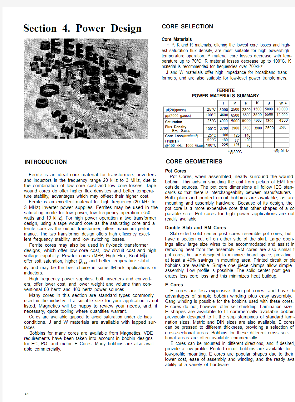
Core Materials
F, P, K and R materials, offering the lowest core losses and high-est saturation flux density, are most suitable for high power/high temperature operation. P material core losses decrease with tem-perature up to 70°C; R material losses decrease up to 100°C. K material is recommended for frequencies over 700kHz.
J and W materials offer high impedance for broadband trans-formers, and are also suitable for low-level power transformers.
FERRITE
POWER MATERIALS SUMMARY
*@80°C+@10kHz CORE GEOMETRIES
Pot Cores
Pot Cores, when assembled, nearly surround the wound bobbin. This aids in shielding the coil from pickup of EMI from outside sources. The pot core dimensions all follow IEC stan-dards so that there is interchangeability between manufacturers. Both plain and printed circuit bobbins are available, as are mounting and assembly hardware. Because of its design, the pot core is a more expensive core than other shapes of a com-parable size. Pot cores for high power applications are not readily available.
Double Slab and RM Cores
Slab-sided solid center post cores resemble pot cores, but have a section cut off on either side of the skirt. Large open-ings allow large size wires to be accommodated and assist in removing heat from the assembly. RM cores are also similar to pot cores, but are designed to minimize board space, providing at least a 40% savings in mounting area. Printed circuit or plain bobbins are available. Simple one piece clamps allow simple assembly. Low profile is possible. The solid center post gen-erates less core loss and this minimizes heat buildup.
E Cores
E cores are less expensive than pot cores, and have the advantages of simple bobbin winding plus easy assembly. Gang winding is possible for the bobbins used with these cores.
E cores do not, however, offer self-shielding. Lamination size E shapes are available to fit commercially available bobbins previously designed to fit the strip stampings of standard lami-nation sizes. Metric and DIN sizes are also available. E cores can be pressed to different thickness, providing a selection of cross-sectional areas. Bobbins for these different cross sec-tional areas are often available commercially.
E cores can be mounted in different directions, and if desired, provide a low-profile. Printed circuit bobbins are available for low-profile mounting. E cores are popular shapes due to their lower cost, ease of assembly and winding, and the ready avail-ability of a variety of hardware.
4.1
EC, ETD and EER Cores EP Cores
These shapes are a cross between E cores and pot cores. Like E cores, they provide a wide opening on each side. This gives ade-quate space for the large size wires required for low output voltage switched mode power supplies. It also allows for a flow of air which keeps the assembly cooler. The center post is round, like that of the pot core. One of the advantages of the round center post is that the winding has a shorter path length around it (11% shorter) than the wire around a square center post with an equal area. This reduces the losses of the windings by 11% and enables the core to handle a higher output power. The round center post also elimi-nates the sharp bend in the wire that occurs with winding on a square center post.
EP Cores are round center-post cubical shapes which enclose the coil completely except for the printed circuit board terminals. The particular shape minimizes the effect of air gaps formed at mating surfaces in the magnetic path and provides a larger volume ratio to total space used. Shielding is excellent.
Toroids
Toroids are economical to manufacture; hence, they are least costly of all comparable core shapes. Since no bobbin is required, accessory and assembly costs are nil. Winding is done on toroidal winding machines. Shielding is relatively good.
PQ Cores
PQ cores are designed especially for switched mode power supplies. The design provides an optimized ratio of volume to winding area and surface area. As a result, both maximum in-ductance and winding area are possible with a minimum core size. The cores thus provide maximum power output with a mini-mum assembled transformer weight and volume, in addition to taking up a minimum amount of area on the printed circuit board. Assembly with printed circuit bobbins and one piece clamps is simplified. This efficient design provides a more uniform cross-sectional area; thus cores tend to operate with fewer hot spots than with other designs.Summary
Ferrite geometries offer a wide selection in shapes and sizes. When choosing a core for power applications, parameters shown in Table 1 should be evaluated.
TABLE 1
FERRITE CORE COMPARATIVE GEOMETRY CONSIDERATIONS
Pot Double E EC, ETD,PQ EP
Core Slab,Core EER Core Core Toroid
RM Cores Cores
See Catalog Section67-8111210913
Core Cost high high low medium high medium very low Bobbin Cost low low low medium high high none Winding Cost low low low low low low high Winding Flexibility good good excellent excellent good good fair Assembly simple simple simple medium simple simple none Mounting Flexibility **good good good fair fair good poor
Heat Dissipation poor good excellent good good poor good Shielding excellent good poor poor fair excellent good
** Hardware is required for clamping core halves together and mounting assembled core on a circuit board or chassis.
4.2
TRANSFORMER CORE SIZE SELECTION
The power handling capacity of a transformer core can be determined by its WaAc product, where Wa is the available core window area, and Ac is the effective core cross-sectional area.
FIGURE 1
The WaAc/power-output relationship is obtained by starting
with Faraday’s Law:
E = 4B Ac Nf x 10–8 (square wave)E = 4.44 BAc Nf x 10–8 (sine wave)Where:
(1)(1a)E = applied voltage (rms)
B = flux density in gauss
Ac = core area in cm2
N = number of turns
f = frequency in Hz
Aw = wire area in cm2Wa = window area in cm2:core window for toroids
bobbin window for other cores C = current capacity in cm2/amp K = winding factor I = current (rms)P i = input power P o = output power e = transformer efficiency Solving (1) for NAc
NAc=E x 10
8
4Bf
The winding factor (2)
K=NAw thus N=
KWa and NAc=
KWaAc (3)
Wa
Aw
Aw
Combining (2) and (3) and solving for WaAc:WaAc =E Aw x108
, where WaAc=cm 4
(4)
4B fK
In addition:
C=Aw/l or Aw=IC e=P o /P i P i =El
Thus:
E Aw = EIC = P i C = P o C/e
Substituting for EAw in (4), we obtain:
Assuming the following operational conditions:C = 4.05 x 10⁻³cm2/Amp (square wave) and
2.53 x 10⁻³cm2/Amp (sine wave) for toroids C = 5.07 x 10⁻³cm2/Amp (square wave) and
3.55 x 10⁻³cm2/Amp (sine wave) for pot cores and E-U-I cores.
e = 90% for transformers
e = 80% for inverters (including circuit losses)
K = .3 for pot cores and E-U-I cores (primary side only)K = .2 for toroids (primary side only)With larger wire sizes, and/or higher voltages, these K fac-tors may not be obtainable. To minimize both wire losses and core size, the window area must be full.
NOTE: For Wire Tables and turns/bobbin data, refer to pages 5.9, 5.10
and 5.11.
We obtain the basic relationship between output power and the WaAc product:
WaAc =
k’ Po x 108
, Where k’ =
C Bf
4eK For square wave operation
k’=.00633 for toroids, k'=.00528 for pot cores, k'=.00528 for E-U-I cores
If we assume B to be 2000 gauss, we obtain the graphs on Figure 7, page 4.7 showing output power as a function of WaAc and frequency.
Cores selected using these graphs will generate the follow-ing temperature increases for 20 KHz square wave operation @ 2000 gauss (typical inverter output transformer conditions):
WaAc range
? T range
< 1.01< 30°C
1.01 to 4.530°C to 60°C 4.5 to 15.260°C to 90°C
These temperatures can be reduced, as needed, by lowering the flux density or frequency, increasing the wire diameter, or using special cooling techniques.
Due to the wide range of core sizes and operational condi-tions, it is essential that your design be evaluated for tem-perature rise before the final core size is chosen.
CIRCUIT TYPES
Some general comments on the different circuits are:The push-pull circuit is efficient because it makes bidirectional use of a transformer core, providing an output with low ripple.However, circuitry is more complex, and the transformer core saturation can cause transistor failure if power transistors have unequal switching characteristics.
Feed forward circuits are low in cost, using only one transis-tor. Ripple is low because relatively steady state current flows in the transformer whether the transistor is ON or OFF.
The flyback circuit is simple and inexpensive. In addition, EMI problems are less. However, the transformer is larger and ripple is higher.
WaAc=
P o C x 108
(5)
4eB fK
4.3
TABLE 2 CIRCUIT TYPE SUMMARY
For ferrite transformers, at 20 kHz, it is common practice to apply equation (4) using a flux density (B) level of ± 2 kG maxi-mum. This is illustrated by the shaded area of the Hysteresis Loop in figure 2b. This B level is chosen because the limiting factor in selecting a core at this frequency is core loss. At 20 kHz, if the transformer is designed for a flux density close to saturation (as done for lower frequency designs), the core will develop an excessive temperature rise. Therefore, the lower operating flux density of 2 kG will usually limit the core losses,thus allowing a modest temperature rise in the core.
Above 20 kHz, core losses increase. To operate the SPS at higher frequencies, it is necessary to operate the core flux levels lower than ± 2 kg. Figure 3 shows the reduction in flux levels for MAGNETICS “P” ferrite material necessary to maintain con-stant 100mW/cm3 core losses at various frequencies, with a max-imum temperature rise of 25°C.
Advantages Medium to high power Efficient core use Ripple and noise low Medium power Low cost
Ripple and noise low Lowest cost
Few components
Disadvantages More c omponents
Core use inefficient
Ripple and noise high Regulation poor Output power limited (< 100 watts)
Circuit Push-pull
Feed forward Flyback
PUSH-PULL CIRCUIT
A typical push-pull circuit is shown in Figure 2a. The input signal is the output of an IC network, or clock, which switches the transistors alternately ON and OFF. High frequency square waves on the transistor output are subsequently rectified,producing dc.
FIGURE 2a
TYPICAL PUSH-PULL SPS CIRCUIT
FIGURE 3
Frequency kHz
FIGURE 2b
HYSTERESIS LOOP OF MAGNETIC CORE IN PUSH-PULL CIRCUIT
FEED FORWARD CIRCUIT
FIGURE 4a
TYPICAL FEED FORWARD
SPS CIRCUIT
4.4
FIGURE 4b
HYSTERESIS LOOP OF MAGNETIC CORE IN FEED FORWARD CIRCUIT
In the feed forward circuit shown in Figure 4a, the transformer operates in the first quadrant of the Hysteresis Loop. (Fig. 4b).Unipolar pulses applied to the semiconductor device cause the transformer core to be driven from its B R value toward satura-tion. When the pulses are reduced to zero, the core returns to its B R value. In order to maintain a high efficiency, the primary inductance is kept high to reduce magnetizing current and lower wire losses. This means the core should have a zero or mini-mal air gap.
For ferrites used in this circuit, ? B (or B max-B R ) is typically 2400 gauss or B (as applied to Equation 4) is ± 1200 gauss as shown in Figure 4b. In the push-pull circuit, it was recom-mended that the peak flux density in the core should not exceed B = ± 2000 gauss in order to keep core losses small. Because of the constraints of the Hysteresis Loop, the core in the feed forward circuit should not exceed a peak value of B = ± 1200gauss.
Core selection for a feed forward circuit is similar to the push-pull circuit except that B for Equation 4 is now limited to ± 1200 gauss. If the charts in Figure 7 are used, WaAc is selected from the appropriate graph and increased by the ratio of 2000 = 1.67, or by 67%.1200If the transformer operating temperature is above 75°, the value of B will be further reduced. Figure 5 shows the variation of ?B with temperature. Therefore, the recommended ?B value of 2400 (B = ± 1200) gauss has to be reduced, the amount depending on the final projected temperature rise of the device.
FIGURE 5
Core Temperature (°C)
The value of ?B remains virtually unchanged over a large These graphs note the output power vs. core size at various frequency range above 20 kHz. However, at some frequency,frequencies. Core selection is made by determining the amount the adjusted value of B, as shown in Figure 3, will become less of output power required. Using one of the charts in Figure 7,than the B determined by the above temperature considerations find the intersection of the output power and the operating fre-(Figure 5). Above this frequency, the B used to select a core quency line; the vertical projection of this point indicates the core will be the value obtained from Figure 3.
to be used. If the vertical projection of the point is between two
4.5
FLYBACK CIRCUIT
A typical schematic is shown in Figure 6a. Unipolar pulses cause dc to flow through the core winding, moving the flux in the core from
B R towards saturation (Fig. 6b). When the pulses go to zero, the flux travels back to B R as in the feed forward design. However, the difference between the feed forward and the flyback circuit is that the flyback requires the transformer to act as an energy storage device as well as to perform the usual transformer functions. Therefore, to be an effective energy stor-age unit, the core must not saturate and is usually a gapped structure.
FIGURE 6a
TYPICAL FLYBACK REGULATOR
CIRCUIT
FIGURE 6b
HYSTERESIS LOOP OF MAGNETIC
CORE IN FLYBACK CIRCUIT
In most designs, the air gap is large; therefore, B R is small as noted on the Hysteresis Loop in Figure 6b and can be con-sidered zero. The maximum flux density available is approxi-mately 3600. This means ?B is 3600 or B = ± 1800 gauss. Core selection for this circuit can also be done using Equation 4 or the charts in Figure 7 as previously described. The B value in Equation 4 is ± 1800 gauss at 20 kHz and is used until a higher frequency (Figure 3) dictates a lower B is required.
To simplify core selection without using Equation (4) and under the limiting conditions noted above, graphs shown in Fig-ure 7 can be used.
cores, choose the larger one. If, for example, a ferrite pot core is needed for a transformer output power of 20 watts at 20 kHz, the above procedure indicates that the correct pot core is between a 42318-UG and a 42616-UG size. In this example, the large core (42616-UG) would be the better selection.
Above 20 kHz, this procedure is changed as follows. First note the intersection of the horizontal line representing the desired output power and the frequency of operation. The verti-cal line through this intersection intersects the horizontal axis which lists the appropriate WaAc. This factor is based on oper-ating at B = ± 2kG and must be increased inversely in propor-tion to the decreased flux density recommended for the operating frequency (see Figure 3). Using the newly selected WaAc factor on the graph, the vertical line through this point indicates the core to be used in this design.
In the example above (output of 20 watts), if the core is to operate at 50 kHz, the graph indicates a pot core with a WaAc of .117 cm4. Figure 3, however, shows that the flux density at 50 kHz must be reduced to 1600 gauss. Therefore, the ratio
(WaAc) @ 20kHz
equals 2000
or 1.25 The new WaAc at
(WaAc) @ 50kHz1600
50 kHz must be .117 x 1.25 or .146cm4. From the graph, the larger WaAc value dictates a 42213-UG pot core.GENERAL FORMULA — CORE SELECTION FOR DIFFERENT TOPOLOGIES
The following formula has been gained from derivations in Chapter 7 of A. I. Pressman’s book, “Switching Power Supply Design” (see Reference No. 14, page 14.1).
P
o
D
cma
WaAc =
K
t
B max?
WaAc = Product of window area and core area (cm 4)
P
o
= Power Out (watts)
D cma= Current Density (cir. mils/amp)
B
max
= Flux Density (gauss)
?= frequency (hertz)
K t= Topology constant (for a space factor of 0.4):
Forward converter = .0005Push-pull = .001
Half-bridge = .0014Full-bridge = .0014
Flyback = .00033 (single winding)
Flyback = .00025 (multiple winding)
For individual cores, WaAc is listed in this catalog under “Mag-netic Data.”
Choice of B max at various frequencies, D cma and alternative transformer temperature rise calculation schemes are also dis-cussed in Chapter 7 of the Pressman book.
Table 3 - FERRITE CORE SELECTION BY AREA PRODUCT DISTRIBUTION
W a A * PC RS, DS RM, EP RM PQ EE
c EE,EE, El EC ETD,UU,TC (cm4)HS SOLID LAM EEM,EFD PLANAR EER UI
.001 4070441309(E) 40601
.0024090540707(EP)4090440603
40906
.004
.0074110741110(RM)40705
.0104140841010(EP)412034110641003 (RS, DS)(UI)41005
.0204140841510(RM)41510412054120841106(U)40907
41313(EP)4120941303
41515
41707
.04041812(RM)418124170941206
4211041305
.070418114231141717(EP)426104180841306 (RS, DS, HS)41605
.100422134231842316(RM)42316420164181042216(E)
(HS)4261442510
.200426164231842819(RM)420204221143618(El)4251541809 (RS, DS)42120(EP)426204281043208(El)(UI)42206
426164321443009
(RS, DS, HS)42523
.400430194281942625425204251543618(E)42207 (RS, DS, HS)4300743208(E)
.7004301943723(RM)4322043515430134351742220(U)42507
42512(U)
42515(U)
1.0043622436224372343230443174352044308(El)441194343442530(U)42908
(RS, DS, HS)4352443521(EER)
44011
2.00442294422943535447214402044308(E)452244393944119(U)43610
44529(RS, DS, HS)4492445810(El)44216(EER)44121(U)43615
4444443813
45032
4.0044040457244402246410(El)4494944125(U)44416
4502144130(U)
7.004552845810(E)
4601646409(E)
10.004553046410(E)4703544916
4722844925
46113 20.00480204705447313 40.0049938(E)48613 10049925(U)
* Bobbin window & core area product. For bobbins other than those in this catalog, W a A c may need to be recalculated.
4.6
Figure 7
For a given P o choose a core size which has a WaAc equal to or greater than the value obtained from the graph. If the frequency is variable, use the lowest operating frequency.
These curves are based on bi-polar operations.
The power handling capacity of a given core is directly proportional to the flux level (B), the frequency (f), and the current density (1/C);thus the WaAc needed for your operational conditions can be readily obtained using these graphs. Note: These curves are based on B = 2000. At frequen-cies of 40 to 100 kHz, it may be more desirable to use B = 1000.If so, double the WaAc required.
For saturating square wave invert-For center tap transformers, the ers, divide WaAc by 1.8 for F or P wire size can be reduced 30%materials. G, J, & W materials are (one wire size), but the WaAc not recommended for this type values should be increased by application. Saturating inverters 20% if the primary is push-pull,with P o values > 50 watts or and 40% if both primary and frequencies > 10 kHz are not secondary are push-pull.
recommended due to excessively high ? T values.
4.7
Table 4
FERRITE CORE SELECTION LISTED BY TYPICAL POWER HANDLING CAPACITIES (WATTS)
(F, P and R Materials) (For push-pull square wave operation, see notes below).
42107
4130342110
5 8 11
21
41808
42311 41811-PC 41306 41717 42610-PQ 42311-RS, 42809-RM 4160542216-EC
12 18 27 53 41810, 42211 42016
42316-RM 42614-PQ
1320305942510
1522
32
62
42213-PC
18 28 43 84 42020
42318 42318-RS
42106
43618-E, I
19 30 48 94 42616
41809 42120 43208-E, I
44008-E, I 26425811342810,
4252042206
28456512742515
42819-RM
4210930497013742620
42616-PC
42207
33
53
80
156
43019
43618-EC 40 61 95 185 43007
43019-RS
43205
44008-EC 42 70 100 195 42625
43208-EC 48751102154301342212,
4250760100150
29342530, 4300943517 (EC35) 4322043019-PC
43515 (E375)
43723-RM
70 110 170 332
43434 (ETD34)
43622
42908
44308-E, I
10516023546044011 (E40)
11019025048043230
43622-PC 12019527052544119 (EC41)
13020529057043524, 4352043521
43806
14021534066344317 (E21)
42915,
4311315024038074143939 (ETD39)
44308-EC
19030047091744229
43610
20031050097544721 (E625)45032
220350530103443535
43813230350550107344020
(42/15)44216
260400600117043615
280430
650
1268
45021 (E50), 4492445224
(EC52)44229-PC 300 450 700 1365 44022
(42/20) 44444 (ETD44) 44529-PC
45810-E, I
340550850165844040
360580870169743825410 650 1000 1950 45724 (E75) 44949 (ETD49)
44416 46410-E, I 5508001300253545528 (55/21)
46016
(E60)4471545810-EC
65010001600312044916, 44920
70011001800351045530
(55/25)46409-EC 85013001900370544925
46410-EC 90015002000390047035 (EC70)100016002500487545959 (ETD59)
46113
100017002700526547228
140025003200624044932160026003700721547313
2000
3000
4600
897048020
47054
2800 4200 6500 12675
48613 49938-EC
117001900026500
51500
49925 (U)
Above is for push-pull converter. De-rate by Note: Assuming Core Loss to be Approximately 100mW/cm3,
a factor of 3 or4 for flyback. De-rate by a B Levels Used in this Chart are:
factor of 2 for feed-forward converter.
@ 20 kHz - 2000 gauss @ 50 kHz - 1300 gauss @ 100 kHz - 900 gauss @ 250 kHz - 700 gauss
See page 4.6 - Area Product Distribution
4.8
41709413134120641408-PC
417077
432
Cores Cores Toroids Cores
Cores Cores
U Cores
E-Cores 250 kHz
kHs 10050 kHz 20 kHz
Planar EP TC RS-RM-PC DS
PQ EC - ETD,
@f=@f=@f=@f=Low Profile,Wattage
TEMPERATURE CONSIDERATIONS
The power handling ability of a ferrite transformer is limited by either the saturation of the core material or, more commonly, the temperature rise. Core material saturation is the limiting factor when
the operating frequency is below 20kHz. Above this frequency tem-perature rise becomes the limitation.
V x 108
Np =p
V
N s
=Np
s
Temperature rise is important for overall circuit reliability. Staying below a given temperature insures that wire insulation is valid, that nearby active components do not go beyond their rated tem-perature, and overall temperature requirements are met. Tempera-ture rise is also very important from the core material point of view. As core temperature rises, core losses can rise and the maximum saturation flux density decreases. Thermal runaway can occur causing the core to heat up to its Curie temperature resulting in a loss of all magnetic properties and catastrophic failure. Newer fer-rite power materials, like P and R material, attempt to mitigate this problem by being tailored to have decreasing losses to tempera-ture of 70°C and 100°C respectively.
Core Loss – One of the two major factors effecting temperature rise is core loss. In a transformer, core loss is a function of the voltage applied across the primary winding. In an inductor core, it is a function of the varying current applied through the inductor. In either case the operating flux density level, or B level, needs to be determined to estimate the core loss. With the frequency and B level known, core loss can be estimated from the material core loss curves. A material loss density of 100mw/cm3 is a common operating point generating about a 40°C temperature rise. Oper-ating at levels of 200 or 300 mw/cm3 can also be achieved, al-though forced air or heat sinks may need to be used.
Winding Considerations – Copper loss is the second major con-tributor to temperature rise. Wire tables can be used as a guide to estimate an approximate wire size but final wire size is dependent on how hot the designer allows the wire to get. Magnet wire is commonly used and high frequency copper loss needs to be con-sidered. Skin effect causes current to flow primarily on the surface of the wire. To combat this, multiple strands of magnet wire, which have a greater surface area compared to a single heavier gauge, are used. Stranded wire is also easier to wind particularly on tor-oids. Other wire alternatives, which increase surface areas, are foil and litz wire. Foil winding allows a very high current density. Foil should not be used in a core structure with a significant air-gap since excessive eddy currents would be present in the foil. Litz wire is very fine wire bundled together. It is similar to stranded wire except the wire is woven to allow each strand to alternate between the outside and the inside of the bundle over a given length.TRANSFORMER EQUATIONS
Once a core is chosen, the calculation of primary and secon-dary turns and wire size is readily accomplished.
Core Geometry – The core shape also affects temperature and those that dissipate heat well are desirable. E core shapes dissi-pate heat well. Toroids, along with power shapes like the PQ, are satisfactory. Older telecommunication shapes, such as pot cores or RM cores, do a poor job of dissipating heat but do offer shield-ing advantages. Newer shapes, such as planar cores, offer a large flat surface ideal for attachment of a heat sink.
4.9
EMI FILTERS
Switch Mode Power Supplies (SMPS) normally generate excessive high frequency noise which can affect electronic equipment like computers, instruments and motor controls connected to these same power lines. An EMI Noise Filter inserted between the power line and the SMPS eliminates this type of interference (Figure 8). A differential noise filter and a common mode noise filter can be in series, or in many cases, the common mode filter is used alone.
Figure 10
Figure 8
Common Mode Filter
In a CMN filter, each winding of the inductor is connected in series with one of the input power lines. The connections and phasing of the inductor windings are such that flux created by one winding cancels the flux of the second winding. The insertion impedance of the inductor to the input power line is thus zero,except for small losses in the leakage reactance and the dc resistance of the windings. Because of the opposing fluxes, the input current needed to power the SMPS therefore will pass through the filter without any appreciable power loss.
Common mode noise is defined as unwanted high frequency current that appears in one or both input power lines and returns to the noise source through the ground of the inductor. This current sees the full impedance of either one or both windings of the CMN inductor because it is not canceled by a return https://www.360docs.net/doc/d36498848.html,mon mode noise voltages are thus attenuated in the windings of the inductor, keeping the input power lines free from the unwanted noise.
Choosing the Inductor Material
A SMPS normally operates above 20kHz. Unwanted noises generated in these supplies are at frequencies higher than 20kHz,often between 100kHz and 50MHz. The most appropriate and cost effective ferrite for the inductor is one offering the highest impedance in the frequency band of the unwanted noise.Identifying this material is difficult when viewing common parameters such as permeability and loss factor. Figure 9 shows a graph of impedance Z t vs. frequency for a ferrite toroid, J-42206-TC wound with 10 turns.
FREQUENCY
Figure 11
FREQUENCY
Figure 9
FREQUENCY
The wound unit reaches its highest impedance between 1and 10MHz. The series inductive reactance X s and series
resistance R s (functions of the permeability and loss factor o the material) together generate the total impedance Z t .
Figure 10 shows permeability and Ioss factor of the ferrite material in Figure 9 as a function of frequency.The falling off of permeability above 750kHz causes the inductive reactance to fall. Loss factor, increasing with frequency, causes the resis-tance to dominate the source of impedance at high frequencies.
Figure 11 shows total impedance vs. frequency for three different materials. J material has a high total impedance over the range of 1 to 20MHz. It is most widely used for common mode filter chokes. Under 1Mhz, W material has 20-50% more impedance than J. It is often used in place of J when low frequency noise is the major problem. K material can be used
above 2MHz because it produces up to 100% more impedance than J in this frequency range. For filter requirements specified at frequencies above and below 2MHz, either J or W is preferred.Core Shape
Toroids are most popular for a CMN filter as they are inexpensive and have low leakage flux. A toroid must be wound by hand (or individually on a toroid winding machine). Normally a non-metallic divider is placed between the two windings, and the wound unit is epoxied to a printed circuit header for attaching to a pc board.
An E core with its accessories is more expensive than a toroid, but assembly into a finished unit is less costly. Winding E core bobbins is relatively inexpensive. Bobbins with dividers for separating the two windings are available for pc board mounting.
E cores have more leakage inductance, useful for differential filtering in a common mode filter. E cores can be gapped to increase the leakage inductance, providing a unit that will absorb both the common mode and differential unwanted noise.
Additional detailed brochures and inductor design software for this application are available from Magnetics.
4.10
Core Selection
The following is a design procedure for a toroidal, single-layer common mode inductor, see Figure 12. To minimize winding capacitance and prevent core saturation due to asym-metrical windings, a single layer design is often used. This procedure assumes a minimum of thirty degrees of free spacing between the two opposing windings.
The basic parameters needed for common mode inductor design are current (I), impedance (Z s ), and frequency (f). The current determines the wire size. A conservative current density of 400 amps/cm2 does not significantly heat up the wire. A more aggressive 800 amps/cm2 may cause the wire to run hot. Selection graphs for both levels are presented.
The impedance of the inductor is normally specified as a minimum at a given frequency. This frequency is usually low enough to allow the assumption that the inductive reactance,X S , provides the impedance, see Figure 9. Subsequently, the inductance, L S , can be calculated from:
L S X S =
2 πf
(1)
With the inductance and current known, Figures 13 and 14can be used to select a core size based on the LI product,where L is the inductance in mH and I is the current in amps.The wire size (AWG) is then calculated using the following equation based on the current density (C d ) of 400 or 800amps/cm2:
AWG = -4.31 x ln
(
1.889I )
C d
(2)
The number of turns is determined from the core’s A L value as follows:
N =
(
L s x 10 6
A L
)
?
(3)
Design Example
An impedance of 100?is required at 10kHz with a current of 3 amps. Calculating the inductance from equation 1, L S =1.59 mH.
With an LI product of 4.77 at 800 amps/cm2, Figure 14yields the core size for chosen material. In this example, W material is selected to give high impedance up to 1MHZ, see Figure 11. Figure 14 yields the core W-41809-TC. Page 13.2lists the core sizes and A L values. Using an A L of 12,200mH/1000 turns, equation 3 yields N = 12 turns per side. Using 800 amps/cm2, equation 2 yields AWG = 21.
Figure 12: Common mode inductor winding arrangement
Figure 14: Core selection at 800 amps/cm2
CMF, LI vs AP at 400 amps/cm2
L I (millihenry - amps)
Figure 13: Core selection at 400 amps/cm2
CMF, LI vs AP at 800 amps/cm2
L I (millihenry - amps)
4.11
HALL EFFECT DEVICES
Graphical Method
1. Calculate NI/B (amp turns per gauss), knowing the flux operating extremes of ?V/?B or the maximum B sensitivity of the sensor.
2. Using Figure 15, follow the NI/B value from the vertical axis to the diagonal line to choose a ferrite core size. Drop down from the diagonal line to the horizontal axis to determine the gap length. The core sizes indicated on the selector chart take into account gap length versus cross-section dimensions in order to maintain an even flux distribution across the gap under maximum current.
Edwin H. Hall observed the “Hall Effect” phenomenon at Johns Hopkins University in 1897. He monitored the current flowing from top to bottom in a thin rectangular strip of gold foil by measuring the voltages at the geometric center of the left edge and the right edge of the strip. When no magnetic field was present, the voltages were identical. When a magnetic field was present perpendicular to the strip, there was a small voltage difference of a predictable polarity and magnitude. The creation of the transverse electric field, which is perpendicular to both the magnetic field and the current flow, is called the Hall Effect or Hall Voltage.
In metals the effect is small, but in semiconductors,considerable Hall voltages can be developed. Designers should consider using Hall sensors in many applications where mechanical or optical sensors have traditionally been used. To monitor ac or dc current flowing in a wire, the wire is wrapped around a slotted ferromagnetic core, creating an electro-magnet. The strength of the resulting magnetic field is used by the Hall sensor, inserted in the air gap, to measure the magnitude and direction of current flowing in the wire.
Toroid Gapping
Ferrite cores are a ferromagnetic ceramic material. As such, they exhibit a very high hardness characteristic, they are very brittle, and they do not conduct heat very efficiently.Machining a slot into one side of a ferrite toroid can be a difficult process. Special techniques must be used to prevent chipping, cracking, or breaking of the cores.
Diamond bonded-tool machining is the preferred method of cutting ferrite. The bonded diamond particle size should be approximately 100 to 170 mesh (150 to 90 μm). The peripheral speed of the cutting wheel should be 5000 to 6000feet/minute (1500 to 1800 meters/minute). The depth of the cut may be as deep as 1” (25 mm), but in order to minimize residual stress, the cut should be limited to a maximum of 0.250” (6 mm) per pass, the smaller the better. During all cutting, the wheel and core should be flooded with ample amounts of coolant water to provide a lubricant as well as remove heat buildup that would cause thermal stress cracking of the core.
Gapped Toroid Selector Chart
Core Selection
In all cases, the effective permeability of a gapped core will be a function of the size of the air gap and the initial permeability of the core material. Once the gap becomes greater than a few thousandths of an inch, the effective permeability is determined essentially by the air gap.
Analytical Method
1. Determine the flux operating extremes based on either the ?V/?B of the circuit (volts/gauss), or the maximum flux sensitivity (gauss) of the sensor (as provided by the sensor data sheet).
2. Choose a core based on the maximum or minimum dimension requirements to allow windings, and based on the core cross-section dimensions. The cross-section dimensions should be at least twice the gap length to ensure a relatively homogeneous flux distribution bridging the gap.
3. Calculate the maximum required μe for the core:
μe =
B l e .4πN I
(1)
where: B = flux density (gauss)
l e = path length (cm)N = turns
I = current (amps peak)
4. Calculate the minimum required gap length (inches):
l
g
=l e
(
1-
1)(
0.3937)
μe
μi
(2)
where: l g = gap length (inches)
l e = path length (cm)
μe = effective permeability μi = initial permeability
5. If the minimum required gap is greater than the sensor thickness, ensure that the cross-section dimensions (length and width) are at least twice the gap length. If not, choose a larger core and recalculate the new gap length.
Gap Length (inches)
Figure 15: Hall Effect Device, Core Selector Chart
4.12
INDUCTOR CORE SIZE SELECTION (using core selector charts)DESCRIPTION
A typical regulator circuit consists of three parts: transistor switch, diode clamp, and an LC filter. An unregulated dc volt-age is applied to the transistor switch which usually operates at a frequency of 1 to 50 kilohertz. When the switch is ON, the input voltage, E in , is applied to the LC filter, thus causing cur-rent through the inductor to increase; excess energy is stored in the inductor and capacitor to maintain output power during the OFF time of the switch. Regulation is obtained by adjusting the ON time, t on , of the transistor switch, using a feedback sys-tem from the output. The result is a regulated dc output,expressed as:
E out =E in t on f
(1)
COMPONENT SELECTION
The switching system consists of a transistor and a feedback from the output of the regulator. Transistor selection involves two factors — (1) voltage ratings should be greater than the max-imum input voltage, and (2) the frequency cut-off characteris-tics must be high compared to the actual switching frequency to insure efficient operation. The feedback circuits usually in-clude operational amplifiers and comparators. Requirements for the diode clamp are identical to those of the transistor. The de-sign of the LC filter stage is easily achieved. Given (1) maximum and minimum input voltage, (2) required output, (3) maximum allowable ripple voltage, (4) maximum and minimum load cur-rents, and (5) the desired switching frequency, the values for the inductance and capacitance can be obtained. First, off-time (t off ) of the transistor is calculated.
The value calculated for ?i is somewhat arbitrary and can be adjusted to obtain a practical value for the inductance.The minimum capacitance is given by
C = ?i/8f min ?e o
(6)
Finally, the maximum ESR of the capacitor is
ESR max = ?e o /?i
(7)INDUCTOR DESIGN
Ferrite E cores and pot cores offer the advantages of decreased cost and low core losses at high frequencies. For switching regulators, F or P materials are recommended be-cause of their temperature and dc bias characteristics. By add-ing air gaps to these ferrite shapes, the cores can be used efficiently while avoiding saturation.
These core selection procedures simplify the design of induc-tors for switching regulator applications. One can determine the smallest core size, assuming a winding factor of 50% and wire current carrying capacity of 500 circular mils per ampere.Only two parameters of the design applications must be known:(a) Inductance required with dc bias (b) dc current
https://www.360docs.net/doc/d36498848.html,pute the product of LI2 where:
L = inductance required with dc bias (millihenries)I = maximum dc output current - I o max + ?i 2. Locate the LI2 value on the Ferrite Core Selector charts on pages 4.15 to 4.18. Follow this coordinate in the intersection with the first core size curve. Read the maximum nominal in-ductance, A L , on the Y-axis. This represents the smallest core size and maximum A L at which saturation will be avoided.3. Any core size line that intersects the LI2 coordinate repre-sents a workable core for the inductor if the core’s A L value is less than the maximum value obtained on the chart.
4. Required inductance L, core size, and core nominal induc-tance (A L ) are known. Calculate the number of turns using
where L is in millihenries
t off = (1 – E out /E in max ) /f
(2)
When E in decreases to its minimum value,
f min = (1 – E out /E in min ) /t off
(3)With these values, the required L and C can be calculated.Allowing the peak to peak ripple current (?i) through the in-ductor to be given by
5. Choose the wire size from the wire table on page 5.9 using 500 circular mils per amp.
?i = 2 I o min
(4)
the inductance is calculated using
L = E out t off / ?i
(5)
4.13
Example.
Choose a core for a switching regulator with the following
requirements:
E o= 5 volts
?e o= .5 volts
I o max= 6 amps
I o min= 1 amp
E in min= 25 volts
E in max= 35 volts
f= 20 KHz
1. Calculate the off-time and minimum switching, f
min, of the
transistor switch using equations 2 and 3.
t off= (1 – 5/35)/20,000 = 4.3 × 10⁻⁵seconds and
f min= (1 – 5/25)/4.3 × 10–5seconds = 18,700 Hz.
2. Let the maximum ripple current, ?i, through the inductor be
?i = 2(1) = 2 amperes by equation 4.
3. Calculate L using equation 5.
L = 5 (4.3 × 10⁻⁵) /2 = .107 millihenries
4. Calculate C and ESR max using equations 6 and 7.
C = 2/8 (18700) (.5) = 26.7 μ farads
and ESR max = .5/2 = .25 ohms
5. The product of LI2 = (.107) (8)2 =
6.9 millijoules.
6. Due to the many shapes available in ferrites, there can be
several choices for the selection. Any core size that the LI2 coor-
dinate intersects can be used if the maximum A L is not exceeded.
Following the LI2 coordinate, the choices are:
(a) 45224 EC 52 core,A L315
(b) 44229 solid center post core,A L315
(c) 43622 pot core,A L400
(d) 43230 PQ core,A L250
7. Given the A L, the number of turns needed for the required
inductance is:
A L Turns
25021
31519
40017
8. Use #14 wire.
Note: MAGNETICS?Molypermalloy and Kool Mu?powder cores
have a distributed air gap structure, making them ideal for
switching regulator applications. Their dc bias characteristics
allow them to be used at high drive levels without saturating.
Information is available in catalogs MPC-1.0, KMC-2.1 and
Brochure SR-IA.
FOR REFERENCES, See page 14.1
4.14
Ferrite DC Bias Core Selector Charts
LI2 (millijoules)
LI2 (millijoules)
A-40903B-40704C-40905D-41107E-41408F-41811G-42213H-42616J-43019K-43622L-44229M-44529
A-41408 (RS)B-42311 (DS, RS)42318 (DS, RS)C-42616 (DS)D- 43019 (DS, RS)E-43622 (DS)F-44229 (DS)
A-40707(EP7)41010(EP10)41110(RM4)B-41313(EP13)C-41510(RM5)D-41717(EP17)E-41812(RM6)F- 42316 (RM8)G-42120(EP20)H-42809(RM10 planar)42819 (RM10)J- N43723 (RM12)
4.15
LI 2 (millijoules)
0.001
0.01
0.1110
A L (m H /1000 t u r n s )
100300500700900110013000
2004006008001000
1200
Ferrite DC Bias Core Selector Charts
Ll2 (millijoules)
A-4201642020B-42614C-42610426204262543214D-4322043230E-4353544040
Ll2 (millijoules)
A-41203 (EE)B-41707 (EE)C-41808 (EE)D-42510 (EE)
E-43009 (EE)43515 (EE)F-44317 (EE)G-44721 (EE)H-45724 (EE)
A-40904 (EE)B-41208 (EE)41209 (EE)C-41205 (EE)42211 (EE)D-42515 (EE)E-41810 (EE)43007 (EE)
F-43524 (EE)G-42530 (EE)43520 (EE)H-42520 (EE)J-42810 (EE)43013 (EE)
Ll2 (millijoules)
4.16
0.01
0.1
1
10
100
A L (m H /1000 t u r n s )
1003005007009001100130002004006008001000
1200
Ferrite DC Bias Core Selector Charts
Ll2 (millijoules) Ll2 (millijoules)A-42110 (EE)
B-41709 (EE)
C- 41805 (EE, El)
D- 42216 (EE, El)
E- 44008 (EE, El)
F- 43208 (EE, El)
43618 (EE, El)
A-44016(EE)F-45528(EE)
B-44011(EE)45530(EE)
C-44020(EE)47228(EE)
D-44308(EE,El)48020(EE)
E-44022(EE)G-46410(EE) 44924(EE)H-49938(EE, El) 45021(EE)
46016(EE)
A- 43517
B- 44119
C- 45224
D- 47035
4.17LI2 (millijoules)
Ferrite DC Bias Core Selector Charts
LI2 (millijoules) Ll2 (millijoules)A-43434(ETD34)
B-43521(EER35L)
C-43939(ETD39)
D-44216(EER42)
44444(ETD44)
E-44949(ETD49)
F-47054
G-45959(ETD59)
A-41309(EEM12.7)
40906
B-42110
41515(EFD15)
C-41709
D-42523(EFD25)
4.18
Graph 4: For Gapped Applications — DC Bias Data
μe vs. H
H (Ampere-turns/cm)
(See bottom of graph for Oersteds)
H(OERSTED)
(See top of graph for Ampere-turns/cm)
H
The above curves represent the locus of points up to which effective permeability remains constant. They show the maximum allowable DC bias, in ampere-turns, without a reduction in inductance. Beyond this level, inductance drops rapidly.
μe
Example: How many ampere-turns can be supported by an R-42213-A-315 pot core without a reduction in inductance value?
e = 3.12 cm μe = 125
Maximum allowable H = 25 Oersted (from the graph above)NI (maximum) = .8 x H x e = 62.4 ampere-turns
OR (Using top scale, maximum allowable H = 20 A-T/cm.)NI (maximum) = A-T/cm x e
= 20 x 3.12= 62.4 A-T
A e = effective cross sectional area (cm2)A L =
inductance/1000 turns (mH)μi = initial permeability g = gap length (cm)
4.19
Section 5. Low Level Applications – Pot Cores
The information contained in this section is primarily concerned dimensions, accessories, and other important design criteria. Stan-with the design of linear inductors for high frequency LC tuned cir-dard Q curves are available on special request, if needed.
cuits using Ferrite Pot Cores. Magnetics has arranged the data in The data presented in this section are compiled mainly for select-this section for ease in (1) determining the optimum core for these ing cores for high Q resonant LC circuits. However, much of this LC circuits and (2) ordering the items necessary for any particular information can also be used to design pot cores into many other Pot Core assembly.applications, including high frequency transformers, chokes, and Featured are magnetic data, temperature characteristics, core other magnetic circuit elements.
Pot Core Assembly
A ferrite pot core assembly includes the following items:
(1) two matched pot core halves
(2) bobbin on which the coils are wound
(3) tuning assembly
(4) a clamp for holding the core halves together
5.1
磁芯材料知识
磁芯材料知識 摘要: 1.磁芯材料基本概念 ui值磁芯的初始透磁率,表征材料對于磁力線的容納與傳導能力。(ui=B/ H) AL值:電感系數. 表征CORE成品所具備的幫助線圈產生電感的能力.其數值等于單 1.磁芯材料 基本概念 ui值 磁芯的初始透磁率,表征材料對于磁力線的容納與傳導能力。(ui=B/H) AL值:電感系數. 表征CORE成品所具備的幫助線圈產生電感的能力.其數值等于單匝電感值,單位是nH/N2 . 磁滯回線:1﹕B-H CURVES (磁滯曲線) Bms:飽和磁束密度﹐表征材料在磁化過程中﹐磁束密度趨于飽和狀態的物理量﹐磁感應強度單位﹕特斯拉=104高斯﹒ 我們對磁芯材料慢慢外加電流,磁通密度(磁感應強度)也會跟著增加,當電流加至某一程度時我們會發現磁通密度會增加很慢,而且會趨近一漸進線,當趨近這一漸進線時這個時候的磁通密度我們就稱為的飽和磁通密度(Bms) Bms高:表明相同的磁通需要較小的橫截面積,磁性元件體積小
Brms:殘留磁束密度﹐也叫剩余磁束密度﹐表征材料在磁化過程結束以后﹐外磁場消失﹐而材料內部依然尚存少量磁力線的特性﹒ Hms:能夠使材料達到磁飽和狀態的最小外磁場強度﹐單位﹕A/m=104/2π奧斯特﹒ Hc:矯頑力﹐也叫保持力﹐是磁化過程結束以后﹐外磁場消失,因殘留 磁束密度而引起的剩余磁場強度﹒因為剩余磁場的方向与磁化方向一 致﹐所以﹐必須施加反向的外部磁場﹐才可以使殘留磁束密度減小到 零﹒ 從磁滯回線我們可以看出:剩磁大,表示磁芯ui值高。磁滯回線越傾斜,表示Hms越大磁芯的耐電流大。矯頑力越大,磁芯的功率損耗大。 鐵粉芯: 鐵粉芯是磁芯材料四氧化三鐵的通俗說法,主要成分是氧化鐵,價格比較低,飽和磁感應強度在1.4T左右:磁導率范圍從22-100,初始磁導率ui值隨頻率的變化穩定性好,直流電流疊加性能好,但高頻下消耗高。 該材料可以從涂裝顏色來辨認材質,例如:26材:黃色本體/白色底面,52材:綠色本體/藍色底面。該類材料價格便宜,如果感量不很高,該材料是首選。可以根據感量大小和IDC要求,選擇所需材料,8材耐電
磁芯材料知识
磁芯材料知識 摘要:1.磁芯材料基本概念ui值磁芯的初始透磁率,表征材料對于磁力線的容納與傳導能力。(ui=B/ H)AL值:電感系數. 表征CORE成品所具備的幫助線圈產生電感的能力.其數值等于單 1.磁芯材料 基本概念 ui值 磁芯的初始透磁率,表征材料對于磁力線的容納與傳導能力。(ui=B/ H) AL值:電感系數. 表征CORE成品所具備的幫助線圈產生電感的能力.其數值等于單匝電感值,單位是nH/N2 . 磁滯回線:1﹕B-H CURVES (磁滯曲線) Bms:飽和磁束密度﹐表征材料在磁化過程中﹐磁束密度趨于飽和狀態的物理量﹐磁感應強度單位﹕特斯拉=104高斯﹒ 我們對磁芯材料慢慢外加電流,磁通密度(磁感應強度)也會跟著增加,當電流加至某一程度時我們會發現磁通密度會增加很慢,而且會趨近一漸進線,當趨近這一漸進線時這個時候的磁通密度我們就稱為的飽和磁通密度(Bms)
Bms高:表明相同的磁通需要較小的橫截面積,磁性元件體積小 Brms:殘留磁束密度﹐也叫剩余磁束密度﹐表征材料在磁化過程結束以后﹐外磁場消失﹐而材料內部依然尚存少量磁力線的特性﹒ Hms:能夠使材料達到磁飽和狀態的最小外磁場強度﹐單位﹕A/m=104/ 2π奧斯特﹒ Hc:矯頑力﹐也叫保持力﹐是磁化過程結束以后﹐外磁場消失,因殘留磁束密度而引起的剩余磁場強度﹒因為剩余磁場的方向与磁化方向一致﹐所以﹐必須施加反向的外部磁場﹐才可以使殘留磁束密度減小到零﹒ 從磁滯回線我們可以看出:剩磁大,表示磁芯ui值高。磁滯回線越傾斜,表示Hms越大磁芯的耐電流大。矯頑力越大,磁芯的功率損耗大。 鐵粉芯: 鐵粉芯是磁芯材料四氧化三鐵的通俗說法,主要成分是氧化鐵,價格比較低,飽和磁感應強度在1.4T左右:磁導率范圍從22-100,初始磁導率ui值隨頻率的變化穩定性好,直流電流疊加性能好,但高頻下消耗高。
磁芯参数参看
z变压器基础知识 1、变压器组成: 原边(初级primary side ) 绕组 副边绕组(次级secondary side ) 原边电感(励磁电感)‐‐magnetizing inductance 漏感‐‐‐leakage inductance 副边开路或者短路测量原边 电感分别得励磁电感和漏感 匝数比:K=Np/Ns=V1/V2 2、变压器的构成以及作用: 1)电气隔离 2)储能 3)变压 4)变流 ●高频变压器设计程序: 1.磁芯材料 2.磁芯结构 3.磁芯参数 4.线圈参数 5.组装结构 6.温升校核 1.磁芯材料 软磁铁氧体由于自身的特点在开关电源中应用很广泛。 其优点是电阻率高、交流涡流损耗小,价格便宜,易加 工成各种形状的磁芯。缺点是工作磁通密度低,磁导率 不高,磁致伸缩大,对温度变化比较敏感。选择哪一类 软磁铁氧体材料更能全面满足高频变压器的设计要求, 进行认真考虑,才可以使设计出来的变压器达到比较理 想的性能价格比。 2.磁芯结构 选择磁芯结构时考虑的因数有:降低漏磁和漏感, 增加线圈散热面积,有利于屏蔽,线圈绕线容易,装配 接线方便等。 漏磁和漏感与磁芯结构有直接关系。如果磁芯不需 要气隙,则尽可能采用封闭的环形和方框型结构磁芯。 3.磁芯参数: 磁芯参数设计中,要特别注意工作磁通密度不只是受磁化曲线限制,还要受损耗的限制,同时还与功率传送的工作方式有关。 磁通单方向变化时:ΔB=Bs‐Br,既受饱和磁通密度限制,又更主要是受损耗限制,(损耗引起温升,温升又会影响磁通密度)。工作磁通密度Bm=0.6~0.7ΔB 开气隙可以降低Br,以增大磁通密度变化值ΔB,开气隙后,励磁电流有所增加,但是可以减小磁芯体积。对于磁通双向工作而言: 最大的工作磁通密度Bm,ΔB=2Bm。在双方向变化工作模式时,还要注意由于各种原因造成励磁的正负变化的伏秒面积不相等,而出现直流偏磁问题。可以在磁芯中加一个小气隙,或者在电路设计时加隔直流电容。 4.线圈参数: 线圈参数包括:匝数,导线截面(直径),导线形式,绕组排列和绝缘安排。 导线截面(直径)决定于绕组的电流密度。通常取J为2.5~4A/mm2。导线直径的选择还要考虑趋肤效应。如必要,还要经过变压器温升校核后进行必要的调整。 4.线圈参数: 一般用的绕组排列方式:原绕组靠近磁芯,副绕组反馈绕组逐渐向外排列。下面推荐两种绕组排列形式: 1)如果原绕组电压高(例如220V),副绕组电压低,可以采用副绕组靠近磁芯,接着绕反馈绕组,原绕组在最外层的绕组排列形式,这样有利于原绕组对磁芯的绝缘安排; 2)如果要增加原副绕组之间的耦合,可以采用一半原绕组靠近磁芯,接着绕反馈绕组和副绕组,最外层再绕一半原绕组的排列形式,这样有利于减小漏感。 5.组装结构:
常用磁芯材料总结
常用磁芯材料 (一)粉芯类 1.磁粉芯 可以隔绝涡流,材料适用于较高频率;材料具有低导磁率及恒导磁特性,磁导率随频率的变化也就较为稳定。主要用于高频电感。 常用的磁粉芯有铁粉芯、坡莫合金粉芯及铁硅铝粉芯三种。 (1).铁粉芯 在粉芯中价格最低。磁导率范围从22~100; 初始磁导率me随频率的变化稳定性好;直流电流叠加性能好;但高频下损耗高。 (2).坡莫合金粉芯 坡莫合金粉芯主要有钼坡莫合金粉芯(MPP)及高磁通量粉芯 MPP主要特点是:磁导率范围大,14~550;在粉末磁芯中具有最低的损耗;温度稳定性极佳,在不同的频率下工作时无噪声产生。粉芯中价格最贵。 高磁通粉芯主要特点是:磁导率范围从14~160;在粉末磁芯中具有最高的磁感应强度,最高的直流偏压能力;磁芯体积小。 价格低于MPP。 (3).铁硅铝粉芯 铁硅铝粉芯主要是替代铁粉芯,损耗比铁粉芯低80%,可在8KHz以上频率下使用;导磁率从26~125;在不同的频率下工作时无噪声产生;具有最佳的性能价格比。主要应用于交流电感、输出电感、线路滤波器、功率因素校正电路等。 2. 软磁铁氧体 软磁铁氧体是以Fe2O3为主成分的亚铁磁性氧化物。有Mn-Zn、Cu-Zn、Ni-Zn等几类,其中Mn-Zn铁氧体的产量和用量最大,Mn-Zn铁氧体的电阻率低,一般在100KHZ以下的频率使用。Cu-Zn、Ni-Zn铁氧体在100kHz~10兆赫的无线电频段的损耗小。 由于软磁铁氧体不使用镍等稀缺材料也能得到高磁导率,粉末冶金方法又适宜于大批量生产,因此成本低,又因为是烧结物硬度大、对应力不敏感,在应用上很方便。而且磁导率随频率的变化特性稳定,在150kHz以下基本保持不变。随着软磁铁氧体的出现,磁粉芯的生产大大减少了,很多原来使用磁粉芯的地方均被软磁铁氧体所代替。 综上所述,可以选择Mn-Zn铁氧体作为磁芯的材料。 轴套材料选择
磁材介绍
? Spang & Co 公司分部 开关电源使用的 磁芯
简介 开关电源(SPS)的优点大家都很清 楚。这些装置中所用的各种电路也在文献中 说明得非常清楚。磁芯在开关电源电路中起 重要作用。磁芯可由多种原料经一系列工序 制成,可以有各种形状和大小,如图1所 示。 每种材料都有自己的特性。因此,必须 参考材料特性考察具体情况下对电源磁芯的 要求,从而选择适当磁芯。 本文介绍开关电源磁芯所用的各种磁 性材料、制造方法以及和电源主要部分相 关的有效磁特性。 磁芯可分为以下三种基本类型:(1) 绕帶磁芯,(2)磁粉芯,(3)铁氧体。 图1:各种磁芯。 以下 MAGNETICS 资料详细讲述另外一些磁芯资料,包括材料说明和特性,以及尺寸和特别设计资料: 铁氧体磁芯……………….…………………………….…技术公报FC-601 钼坡莫合金和高磁通磁粉芯.…………………………….技术公报MPP-400 铁硅铝磁粉芯…………….…………………………….…技术公报KMC-2.0 高磁通磁粉芯…………….…………………………….…技术公报HFPC-01 绕帶磁芯…………….…………………………….………技术公报TWC-500 切割型磁芯…………….…………………………….……技术公报MCC-100 电感器磁粉芯设计软件https://www.360docs.net/doc/d36498848.html, 共模电感器设计软件https://www.360docs.net/doc/d36498848.html, 目錄 绕帶磁芯 (1) 磁粉芯 (3) 铁氧体磁芯 (5)
图 2:TWC 剖视图。 绕帶磁芯 图 2 是典型绕帶磁芯的剖视图。这个磁芯由磁合金窄带制成,厚度为 1/2 密尔到 14 密尔。宽度为 1/8” 到若干英寸。金属带首先切成所需宽度,并覆盖上薄的绝缘材料涂层,然后绕制在芯棒上,一圈包着一圈,一直绕到预定厚度。最后一圈通过点焊焊接在前一圈上,防止松开。 绕制时磁芯材料受压,所以会丧失部分磁性。为了恢复这些失去的磁特性,磁芯必须在氢气炉中退火,退火温度接近 1000°C 。 *频率极限是根据处于磁通饱和或接近饱和状态下的材料获得的。频率越高越好,这样磁感应强度就越低-参见正文。 1 MAGNESIL ? 16.5 750 0.012 (3% SiFe ) 0.006 0.004 0.002 100 Hz 250 Hz 1 kHz 2 kHz SUPERMENDUR (铁钴钒合金材料铁钴钒合金材料)) ORTHONOL ? (50% Ni ) 21 940 0.004 0.002 15 500 0.004 0.002 0.001 750 Hz 1.5 kHz 1.5 kHz 4 kHz 8kHZ 坡莫合金 (80% Ni ) 非晶 2605SC (铁基) 7.4 460 15.5 370 0.004 0.002 0.001 0.0005 0.001 4 kHz 10 kHz 20 kHz 40 kHz 20 kHz 非晶 2605-S3 (铁基铁基)) 14 370 0.001 100 kHz 非晶 2714A (钴基钴基)) 5.75 205 0.001 300 kHz kHz 磁材料 饱和饱和磁感应磁感应 强度千高斯 (B m ) 表 1:绕帶磁芯材料的磁特性 居里温度 °C (T C ) 使用使用频率上限频率上限* 带厚带厚((英寸英寸)) 频率
磁芯资料
1.磁性材料的磁化曲线 磁性材料是由铁磁性物质或亚铁磁性物质组成的,在外加磁场H 作用下,必有相应的磁化强度M 或磁感应强度B,它们随磁场强度H 的变化曲线称为磁化曲线(M~H或B~H曲线)。磁化曲线一般来说是非线性的,具有2个特点:磁饱和现象及磁滞现象。即当磁场强度H足够大时,磁化强度M达到一个确定的饱和值Ms,继续增大H,Ms保持不变;以及当材料的M值达到饱和后,外磁场H降低为零时,M并不恢复为零,而是沿MsMr曲线变化。材料的工作状态相当于M~H曲线或B~H曲线上的某一点,该点常称为工作点。 2.软磁材料的常用磁性能参数 饱和磁感应强度Bs:其大小取决于材料的成分,它所对应的物理状态是材料内部的磁化矢量整齐排列。 剩余磁感应强度Br:是磁滞回线上的特征参数,H回到0时的B值。 矩形比:Br∕Bs 矫顽力Hc:是表示材料磁化难易程度的量,取决于材料的成分及缺陷(杂质、应力等)。 磁导率μ:是磁滞回线上任何点所对应的B与H的比值,与器件工作状态密切相关。 初始磁导率μi、最大磁导率μm、微分磁导率μd、振幅磁导率μa、有效磁导率μe、脉冲磁导率μp。 居里温度Tc:铁磁物质的磁化强度随温度升高而下降,达到某一温度时,自发磁化消失,转变为顺磁性,该临界温度为居里温度。它确定了磁性器件工作的上限温度。 损耗P:磁滞损耗Ph及涡流损耗Pe P = Ph + Pe = af + bf2+ c Pe ∝ f2 t2 / ,ρ降低,磁滞损耗Ph的方法是降低矫顽力Hc;降低涡流损耗Pe 的方法是减薄磁性材料的厚度t 及提高材料的电阻率ρ。在自由静止空气中磁芯的损耗与磁芯的温升关系为: 总功率耗散(mW)/表面积(cm2) 3.软磁材料的磁性参数与器件的电气参数之间的转换
各种合金金属磁芯非晶微晶磁芯介绍
各种合金金属磁芯、非晶、微晶磁芯介绍 一、性能特点: 坡莫合金金属磁芯:各类坡莫合金材料有着各自不同的,较硅钢材料与铁氧体优异的典型磁性能,有着较高的温度稳定性和时效稳定性.高初始磁导率类坡莫合金材料(IJ79,IJ85,IJ86)铁芯常制作电流互感器,小信号变压器;高矩形度类坡莫合金材料(IJ51)铁芯常制作磁放大器,双级性脉冲变压器;低剩磁类坡莫合金材料(IJ67h)铁芯常制作中小功率单极性脉冲变压器. 二、非晶磁芯: ⑴铁基非晶铁芯:在几乎所有的非晶合金铁芯中具有最高的饱和磁感 应强度(1.45~1.56T),同时具有高导磁率,低矫顽力,低损耗,低激磁电流和良好的温度稳定性和时效稳定性.主要用于替代硅钢片,作为各种形式,不同功率的工频配电变压器,中频变压器,工作频率从50Hz到10KHz;作为大功率开关电源电抗器铁芯,使用频率可达50KHz. ⑵铁镍基非晶铁芯:中等偏低的饱和磁感应强度(0.75T),高导磁率, 低矫顽力,耐磨耐蚀,稳定性好.常用于取代坡莫合金铁芯作为漏电开关中的零序电流互感器铁芯. ⑶钴基非晶铁芯:在所有的非晶合金铁芯中具有最高的磁导率,同时 具有中等偏低的饱和磁感应强度(0.65T),低矫顽力,低损耗,优异的耐磨性和耐蚀性,良好的温度稳定性和时效稳定性,耐冲击振动.主要用于取代坡莫合金铁芯和铁氧体铁芯制作高频变压器,滤波电感,磁放大器,脉冲变压器,脉冲压缩器等应用在高端领域(军用) 三、微晶磁芯: 较高的饱和磁感应强度(1.1~1.2T),高导磁率,低矫顽力,低损耗及良的稳定性,耐磨性,耐蚀性,同时具有较低的价格,在所有的金属软磁材料芯中具有最佳的性价比,用于制作微晶铁芯的材料被誉为"绿色材料".泛应用于取代硅钢,坡莫合金及铁氧体,作为各种形式的高频(20KHz100KHz)开关电源中的大中小功率的主变压器,控制变压器,波电感,储能电感,电抗器,磁放大器和饱和电抗器铁芯,EMC滤波器共电感和差模电感铁芯,IDSN微型隔离变压器铁芯;也广泛应用于各种类同精度的互感器铁芯. 环型规格范围: 磁芯最大外径:750mm 磁芯最小内径:6mm 磁芯最小片宽:5mm 磁芯最大片宽:40mm (可叠加得到更宽) 其他规格可以根据客户需求订做 四、参考说明: 坡莫合金金属磁芯,非晶,微晶磁芯电磁性能状态: 横磁热处理,低Br,有一定的恒导特性,适用于小功率单极性脉冲变压器,单端开关电源变压器,滤波电感,电抗器; 常规热处理,低Pc,极低的激磁电流;适用于中频变压器; 纵磁热处理,高Br,适用于配电变压器,中频变压器,双端开关电源变压器,大功率双极性脉冲变压器,饱和电抗器及脉冲压缩器. 摘要:结合应用实例,重点介绍了在不同应用场合选用非晶与超微晶材料的种类及其特点,并与其它磁性材料作了对比。关键词:铁基非晶材料;铁基超微晶材料;磁导率;矫顽力;损耗 五、非晶与超微晶材料的应用 磁材料120×60×40磁芯。按照 E=4.44f×Bm×N×Sc×10-4(1)
磁芯材料分析
磁性材料 一. 磁性材料的基本特性 1. 磁性材料的磁化曲线 磁性材料是由铁磁性物质或亚铁磁性物质组成的,在外加磁场H 作用下,必有相应的磁化强度M 或磁感应强度B,它们随磁场强度H 的变化曲线称为磁化曲线(M~H或B~H曲线)。磁化曲线一般来说是非线性的,具有2个特点:磁饱和现象及磁滞现象。即当磁场强度H足够大时,磁化强度M达到一个确定的饱和值Ms,继续增大H,Ms保持不变;以及当材料的M值达到饱和后,外磁场H降低为零时,M并不恢复为零,而是沿MsMr曲线变化。材料的工作状态相当于M~H曲线或B~H曲线上的某一点,该点常称为工作点。 2. 软磁材料的常用磁性能参数 饱和磁感应强度Bs:其大小取决于材料的成分,它所对应的物理状态是材料内部的磁化矢量整齐排列。 剩余磁感应强度Br:是磁滞回线上的特征参数,H回到0时的B值。 矩形比:Br∕Bs 矫顽力Hc:是表示材料磁化难易程度的量,取决于材料的成分及缺陷(杂质、应力等)。 磁导率μ:是磁滞回线上任何点所对应的B与H的比值,与器件工作状态密切相关。 初始磁导率μi、最大磁导率μm、微分磁导率μd、振幅磁导率μa、有效磁导率μe、脉冲磁导率μp。 居里温度Tc:铁磁物质的磁化强度随温度升高而下降,达到某一温度时,自发磁化消失,转变为顺磁性,该临界温度为居里温度。它确定了磁性器件工作的上限温度。 损耗P:磁滞损耗Ph及涡流损耗Pe P = Ph + Pe = af + bf2+ c Pe ∝f2 t2 / ,ρ 降低, 磁滞损耗Ph的方法是降低矫顽力Hc;降低涡流损耗Pe 的方法是减薄磁性材料的厚度t 及提高材料的电阻率ρ。在自由静止空气中磁芯的损耗与磁芯的温升关系为: 总功率耗散(mW)/表面积(cm2) 3. 软磁材料的磁性参数与器件的电气参数之间的转换 在设计软磁器件时,首先要根据电路的要求确定器件的电压~电流特性。器件的电压~电流特性与磁芯的几何形状及磁化状态密切相关。设计者必须熟悉材料的磁化过程并拿握材料的磁性参数与器件电气参数的转换关系。设计软磁器件通常包括三个步骤:正确选用磁性材料;合理确定磁芯的几何形状及尺寸;根据磁性参数要求,模拟磁芯的工作状态得到相应的电气参数。 二、软磁材料的发展及种类 1. 软磁材料的发展 软磁材料在工业中的应用始于19世纪末。随着电力工及电讯技术的兴起,开始使用低碳钢制造电机和变压器,在电话线路中的电感线圈的磁芯中使用了细小的铁粉、氧化铁、细铁丝等。到20世纪初,研制出了硅钢片代替低碳钢,提高了变压器的效率,降低了损耗。直至现在硅钢片在电力工业用软磁材料中仍居首位。到20年代,无线电技术的兴起,促进了高导磁材料的发展,出现了坡莫合金及坡莫合金磁粉芯等。从40年代到60年代,是科学技术飞速发展的时期,雷达、电视广播、集成电路的发明等,对软磁材料的要求也更高,生产出了软磁合金薄带及软磁铁氧体材料。进入70年代,随着电讯、自动控制、计算机等行业的发展,研制出了磁头用软磁合金,除了传统的晶态软磁合金外,又兴起了另一类材料—非晶态软磁合金。2. 常用软磁磁芯的种类 铁、钴、镍三种铁磁性元素是构成磁性材料的基本组元。 按(主要成分、磁性特点、结构特点)制品形态分类: (1) 粉芯类:磁粉芯,包括:铁粉芯、铁硅铝粉芯、高磁通量粉芯(High Flux)、坡莫合金粉芯(MPP)、铁氧体磁芯
磁芯材料(基础)
2.软磁材料的常用磁性能参数 饱和磁感应强度Bs:其大小取决于材料的成分,它所对应的物理状态是材料内部的磁化矢量整齐排列。 剩余磁感应强度Br:是磁滞回线上的特征参数,H回到0时的B值。 矩形比:Br∕Bs 矫顽力Hc:是表示材料磁化难易程度的量,取决于材料的成分及缺陷(杂质、应力等)。 磁导率m:是磁滞回线上任何点所对应的B与H的比值,与器件工作状态密切相关。 初始磁导率mi、最大磁导率mm、微分磁导率md、振幅磁导率ma、有效磁导率me、脉冲磁导率mp。 居里温度Tc:铁磁物质的磁化强度随温度升高而下降,达到某一温度时,自发磁化消失,转变为顺磁性,该临界温度为居里温度。它确定了磁性器件工作的上限温度。 磁滞损耗Ph的方法是降低矫顽力Hc;降低涡流损耗Pe的方法是减薄磁性材料的厚度t及提高材料的电阻率ρ。在自由静止空气中磁芯的损耗与磁芯的温升关系为: 总功率耗散(mW)/表面积(cm2) 3.软磁材料的磁性参数与器件的电气参数的转换 在设计软磁器件时,首先要根据电路的要求确定器件的电压~电流特性。器件的电压~电流特性与磁芯的几何形状及磁化状态密切相关。设计者必须熟悉材料的磁化过程并拿握材料的磁性参数与器件电气参数的转换关系。设计软磁器件通常包括三个步骤:正确选用磁性材料;合理确定磁芯的几何形状及尺寸;根据磁性参数要求,模拟磁芯的工作状态得到相应的电气参数。 二、软磁材料的发展及种类 1.软磁材料的发展 软磁材料在工业中的应用始于19世纪末。随着电力工及电讯技术的兴起,开始使用低碳钢制造电机和变压器,在电话线路中的电感线圈的磁芯中使用了细小的铁粉、氧化铁、细铁丝等。到20世纪初,研制出了硅钢片代替低碳钢,提高了变压器的效率,降低了损耗。直到现在硅钢片在电力工业用软磁材料中仍居首位。到20年代,无线电技术的兴起,促进了高导磁材料的发展,出现了坡莫合金及坡莫合金磁粉芯等。从40年代到60年代,是科学技术飞速发展的时期,雷达、电视广播、集成电路的发明等,对软磁材料的要求也更高,生产出了软磁合金薄带及软磁铁氧体材料。进入70年代,随着电讯、自动控制、计算机等行业的发展,研制出了磁头用软磁合金,除了传统的晶态软磁合金外,又兴起了另一类材料—非晶态软磁合金。 2.常用软磁磁芯的种类 铁、钴、镍三种铁磁性元素是构成磁性材料的基本组元。 按(主要成分、磁性特点、结构特点)制品形态分类: (1)粉芯类:磁粉芯,包括:铁粉芯、铁硅铝粉芯、高磁通量粉芯(HighFlux)、坡莫合金粉 芯(MPP)、铁氧体磁芯 (2)带绕铁芯:硅钢片、坡莫合金、非晶及纳米晶合金 三常用软磁磁芯的特点及应用 (一)粉芯类 1.磁粉芯 磁粉芯是由铁磁性粉粒与绝缘介质混合压制而成的一种软磁材料。由于铁磁性颗粒很小(高频下使用的为0.5~5微米),又被非磁性电绝缘膜物质隔开,因此,一方面可以隔绝涡流,材料适用于较高频率;另一方面由于颗粒之间的间隙效应,导致材料具有低导磁率及恒导磁特性;又由于颗粒尺寸小,基本上不发生集肤现象,磁导率随频率的变化也就较为稳定。主
磁芯材料分析
一.磁性材料的基本特性 1.磁性材料的磁化曲线 磁性材料是由铁磁性物质或亚铁磁性物质组成的,在外加磁场H作用下,必有相应的磁化强度 M或磁感 应强度B,它们随磁场强度 H的变化曲线称为磁化曲线(M?H或B?H曲线)。磁化曲线一般来说是非线性的,具有2个特点:磁饱和现象及磁滞现象。即当磁场强度H足够大时,磁化强度 M达到一个确定的饱 和值Ms,继续增大H , Ms保持不变;以及当材料的 M值达到饱和后,外磁场 H降低为零时,M并不恢复为零,而是沿 MsMr曲线变化。材料的工作状态相当于M?H曲线或B?H曲线上的某一点,该点常称 为工作点。 2.软磁材料的常用磁性能参数 饱和磁感应强度Bs :其大小取决于材料的成分,它所对应的物理状态是材料内部的磁化矢量整齐排列。剩余磁感应强度Br:是磁滞回线上的特征参数,H回到0时的B值。 矩形比:Br / Bs 矫顽力He :是表示材料磁化难易程度的量,取决于材料的成分及缺陷(杂质、应力等)。 磁导率”是磁滞回线上任何点所对应的B与H的比值,与器件工作状态密切相关。 初始磁导率卩、1最大磁导率gm>微分磁导率gd振幅磁导率ga有效磁导率ge脉冲磁导率gp 居里温度Te:铁磁物质的磁化强度随温度升高而下降,达到某一温度时,自发磁化消失,转变为顺磁性,该临界温度为居里温度。它确定了磁性器件工作的上限温度。 损耗P:磁滞损耗Ph及涡流损耗Pe P = Ph + Pe = af + bf2+ e Pe f2 t2 / ,p降低, 磁滞损耗Ph的方法是降低矫顽力 He;降低涡流损耗Pe的方法是减薄磁性材料的厚度 t及提高材料的电阻率p。在自由静止空气中磁芯的损耗与磁芯的温升关系为: 总功率耗散(mW) /表面积(cm2 ) 3.软磁材料的磁性参数与器件的电气参数之间的转换 在设计软磁器件时,首先要根据电路的要求确定器件的电压?电流特性。器件的电压?电流特性与磁芯的几何形状及磁化状态密切相关。设计者必须熟悉材料的磁化过程并拿握材料的磁性参数与器件电气参数的转换关系。设计软磁器件通常包括三个步骤:正确选用磁性材料;合理确定磁芯的几何形状及尺寸;根据磁性参数要求,模拟磁芯的工作状态得到相应的电气参数。 二、软磁材料的发展及种类 1.软磁材料的发展 软磁材料在工业中的应用始于19世纪末。随着电力工及电讯技术的兴起,开始使用低碳钢制造电机和变压 器,在电话线路中的电感线圈的磁芯中使用了细小的铁粉、氧化铁、细铁丝等。到20世纪初,研制岀了硅 钢片代替低碳钢,提高了变压器的效率,降低了损耗。直至现在硅钢片在电力工业用软磁材料中仍居首位。 到20年代,无线电技术的兴起,促进了高导磁材料的发展,岀现了坡莫合金及坡莫合金磁粉芯等。从40 年代到60年代,是科学技术飞速发展的时期,雷达、电视广播、集成电路的发明等,对软磁材料的要求也更高,生产岀了软磁合金薄带及软磁铁氧体材料。进入70年代,随着电讯、自动控制、计算机等行业的发 展,研制岀了磁头用软磁合金,除了传统的晶态软磁合金外,又兴起了另一类材料一非晶态软磁合金。 2.常用软磁磁芯的种类 铁、钻、镍三种铁磁性元素是构成磁性材料的基本组元。 按(主要成分、磁性特点、结构特点)制品形态分类: ⑴粉芯类:磁粉芯,包括:铁粉芯、铁硅铝粉芯、高磁通量粉芯(High Flux )、坡莫合金粉芯(MPP )、
永磁材料基本知识
永磁材料基本知识 1、什么是永磁材料的磁性能,它包括哪些指标? 永磁材料的主要磁性能指标是:剩磁(Jr, Br)、矫顽力(bHc)、内禀矫顽力(jHc)、磁能积(BH)m。我们通常所说的永磁材料的磁性能,指的就是这四项。永磁材料的其它磁性能指标还有:居里温度(Tc)、可工作温度(Tw)、剩磁及内禀矫顽力的温度系数(Brθ, jHcθ)、回复导磁率(μrec.)、退磁曲线方形度( Hk/ jHc)、高温减磁性能以及磁性能的均一性等。 除磁性能外,永磁材料的物理性能还包括密度、电导率、热导率、热膨胀系数等;机械性能则包括维氏硬度、抗压(拉)强度、冲击韧性等。此外,永磁材料的性能指标中还有重要的一项,就是表面状态及其耐腐蚀性能。 2、什么叫磁场强度(H)? 1820年,丹麦科学家奥斯特(H. C. Oersted)发现通有电流的导线可以使其附近的磁针发生偏转,从而揭示了电与磁的基本关系,诞生了电磁学。实践表明:通有电流的无限长导线在其周围所产生的磁场强弱与电流的大小成正比,与离开导线的距离成反比。定义载有1安培电流的无限长导线在距离导线1/2π米远处的磁场强度为1A/m(安/米,国际单位制SI);在CGS单位制(厘米-克-秒)中,为纪念奥斯特对电磁学的贡献,定义载有1安培电流的无限长导线在距离导线0.2厘米远处磁场强度为1Oe(奥斯特),1Oe=1/(4π×103) A/m。磁场强度通常用H表示。 3、什么叫磁极化强度(J),什么叫磁化强度(M),二者有何区别? 现代磁学研究表明:一切磁现象都起源于电流。磁性材料也不例外,其铁磁现象是起源于材料内部原子的核外电子运动形成的微电流,亦称分子电流。这些微电流的集合效应使得材料对外呈现各种各样的宏观磁特性。因为每一个微电流都产生磁效应,所以把一个单位微电流称为一个磁偶极子。定义在真空中每单位外磁场对一个磁偶极子产生的最大力矩为磁偶极矩pm,每单位材料体积内磁偶极矩的矢量和为磁极化强度J,其单位为T(特斯拉,在CGS单位制中,J的单位为Gs,1T=10000Gs)。 定义一个磁偶极子的磁矩为pm/μ0,μ0为真空磁导率,每单位材料体积内磁矩的矢量和为磁化强度M,其SI单位为A/m,CGS单位为Gs(高斯)。 M与J的关系为:J=μ0 M,在CGS单位制中,μ0=1,故磁极化强度与磁化强度的值相等;在SI 单位制中,μ0=4π×10-7 H/m (亨/米)。 4、什么叫磁感应强度(B),什么叫磁通密度(B),B与H,J,M之间存在什么样的关系? 理论与实践均表明,对任何介质施加一磁场H时(该磁场可由外部电流或外部永磁体提供,亦可由永磁体对永磁介质本身提供,由永磁体对永磁介质本身提供的磁场又称退磁场---关于退磁场的概念,见9 Q),介质内部的磁场强度并不等于H,而是表现为H与介质的磁极化强度J 之和。由于介质内部的磁场强度是由磁场H通过介质的感应而表现出来的,为与H区别,称之为介质的磁感应强度,记为B: B=μ0 H+J (SI单位制)(1-1) B=H+4πM (CGS单位制) 磁感应强度B的单位为T,CGS单位为Gs(1T=104Gs)。 对于非铁磁性介质如空气、水、铜、铝等,其磁极化强度J、磁化强度M几乎等于0,故在这些介质中磁场强度H与磁感应强度B相等。 由于磁现象可以形象地用磁力线来表示,故磁感应强度B又可定义为磁力线通量的密度,磁感应强度B和磁通密度B在概念上可以通用。 5、什么叫剩磁(Jr,Br),为什么在永磁材料的退磁曲线上任意测量点的磁极化强度J值和磁感应强度B值必然小于剩磁Jr和Br值? 永磁材料在闭路状态下经外磁场磁化至饱和后,再撤消外磁场时,永磁材料的磁极化强度J 和内部磁感应强度B并不会因外磁场H的消失而消失,而会保持一定大小的值,该值即称为该材
磁芯的种类及应用
磁芯的种类及应用: 1.磁性材料的磁化曲线 磁性材料是由铁磁性物质或亚铁磁性物质组成的,在外加磁场H 作用下,必有相应的磁化强度M 或磁感应强度B,它们随磁场强度H 的变化曲线称为磁化曲线(M~H或B~H曲线)。磁化曲线一般来说是非线性的,具有2个特点:磁饱和现象及磁滞现象。即当磁场强度H足够大时,磁化强度M达到一个确定的饱和值Ms,继续增大H,Ms保持不变;以及当材料的M值达到饱和后,外磁场H降低为零时,M并不恢复为零,而是沿MsMr曲线变化。材料的工作状态相当于M~H曲线或B~H曲线上的某一点,该点常称为工作点。 2.软磁材料的常用磁性能参数 饱和磁感应强度Bs:其大小取决于材料的成分,它所对应的物理状态是材料内部的磁化矢量整齐排列。 剩余磁感应强度Br:是磁滞回线上的特征参数,H回到0时的B值。 矩形比:Br?Bs 矫顽力Hc:是表示材料磁化难易程度的量,取决于材料的成分及缺陷(杂质、应力等)。 磁导率μ:是磁滞回线上任何点所对应的B与H的比值,与器件工作状态密切相关。 初始磁导率μi、最大磁导率μm、微分磁导率μd、振幅磁导率μa、有效磁导率μe、脉冲磁导率μp。 居里温度Tc:铁磁物质的磁化强度随温度升高而下降,达到某一温度时,自发磁化消失,转变为顺磁性,该临界温度为居里温度。它确定了磁性器件工作的上限温度。 损耗P:磁滞损耗Ph及涡流损耗 Pe P = Ph + Pe = af + bf2+ c Pe ∝ f2 t2 / ,ρ降低,磁滞损耗Ph的方法是降低矫顽力Hc;降低涡流损耗Pe 的方法是减薄磁性材料的厚度t 及提高材料的电阻率ρ。在自由静止空气中磁芯的损耗与磁芯的温升关系为: 总功率耗散(mW)/表面积(cm2) 3.软磁材料的磁性参数与器件的电气参数之间的转换 在设计软磁器件时,首先要根据电路的要求确定器件的电压~电流特性。器件的电压~电流特性与磁芯的几何形状及磁化状态密切相关。设计者必须熟悉材料的磁化过程并拿握材料的磁性参数与器件电气参数的转换关系。设计软磁器件通常包括三个步骤:正确选用磁性材料;合理确定磁芯的几何形状及尺寸;根据磁性参数要求,模拟磁芯的工作状态得到相应的电气参数。 一、软磁材料的发展及种类 1. 软磁材料的发展 软磁材料在工业中的应用始于19世纪末。随着电力工及电讯技术的兴起,开始使用低碳钢制造电机和变压器,在电话线路中的电感线圈的磁芯中使用了细小的铁粉、氧化铁、细铁丝等。到20世纪初,研制出了硅钢片代替低碳钢,提高了变压器的效率,降低了损耗。直至现在硅钢片在电力工业用软磁材料中仍居首位。到20年代,无线电技术的兴起,促进了高导磁材料的发展,出现了坡莫合金及坡莫合金磁粉芯等。从40年代到60年代,是科学技术飞速发展的时期,雷达、电视广播、集成电路的发明等,对软磁材料的要求也更高,生产出了软磁合金薄带及软
永磁材料基本知识
永磁材料基本知识 2006 年08 月26 日星期六08:56 1、什么是永磁材料的磁性能,它包括哪些指标? 永磁材料的主要磁性能指标是:剩磁(Jr, Br)、矫顽力(bHc)、内禀矫顽力(jHc)、磁能积(BH)m。我们通常所说的永磁材料的磁性能,指的就是这四项。永磁材料的其它磁性能指标还有:居里温度(Tc)、可工作温度(Tw)、剩磁及内禀矫 顽力的温度系数(Br 0 , jHc 0 )、回复导磁率(卩rec.)、退磁曲线方形度(Hk/jHc)、高温减磁性能以及磁性能的均一性等。 除磁性能外,永磁材料的物理性能还包括密度、电导率、热导率、热膨胀系数等;机械性能则包括维氏硬度、抗压(拉)强度、冲击韧性等。此外,永磁材料的性能指标中还有重要的一项,就是表面状态及其耐腐蚀性能。 2、什么叫磁场强度(H)? 1820 年,丹麦科学家奥斯特(H. C. Oersted)发现通有电流的导线可以使其附近的磁针发生偏转,从而揭示了电与磁的基本关系,诞生了电磁学。实践表明:通有电流的无限长导线在其周围所产生的磁场强弱与电流的大小成正比,与离开导线的距离成反比。定义载有1安培电流的无限长导线在距离导线1/2 n米远处的磁场强度为1A/m(安/米,国际单 位制SI);在CGS单位制(厘米-克-秒)中,为纪念奥斯特对电磁学的贡献,定义载有1安培电流的无限长导线在距离导 线0.2厘米远处磁场强度为1Oe (奥斯特),10e=1/(4 n x 103) A/m。磁场强度通常用H表示。 3、什么叫磁极化强度(J),什么叫磁化强度(M),二者有何区别? 现代磁学研究表明:一切磁现象都起源于电流。磁性材料也不例外,其铁磁现象是起源于材料内部原子的核外电子运动形成的微电流,亦称分子电流。这些微电流的集合效应使得材料对外呈现各种各样的宏观磁特性。因为每一个微电流都产生磁效应,所以把一个单位微电流称为一个磁偶极子。定义在真空中每单位外磁场对一个磁偶极子产生的最大力矩为磁偶极矩pm,每单位材料体积内磁偶极矩的矢量和为磁极化强度J,其单位为T (特斯拉,在CGS单位制中,J的单 位为Gs,1T=10000Gs)。 定义一个磁偶极子的磁矩为pm/卩0,卩0为真空磁导率,每单位材料体积内磁矩的矢量和为磁化强度M其SI单位为 A/m,CGS单位为Gs(高斯)。 M与J的关系为:J=卩0 M在CGS单位制中,卩0=1,故磁极化强度与磁化强度的值相等;在SI单位制中,卩0=4 n X 10-7H/m (亨/ 米)。 4、什么叫磁感应强度(B),什么叫磁通密度(B),B与H,J,M之间存在什么样的关系? 理论与实践均表明,对任何介质施加一磁场H 时(该磁场可由外部电流或外部永磁体提供,亦可由永磁体对永磁介质本身提供,由永磁体对永磁介质本身提供的磁场又称退磁场--- 关于退磁场的概念,见9 Q),介质内部的磁场强度并不 等于H,而是表现为H与介质的磁极化强度J之和。由于介质内部的磁场强度是由磁场H通过介质的感应而表现岀来 的,为与H区别,称之为介质的磁感应强度,记为B: B=^ 0 H+J (SI 单位制)(1-1 ) B=H+4t M (CGS单位制)
电感基本知识(定义分类原理性能参数应用磁芯等主要材料检测)(精)
一、电感器的定义。 1.1 电感的定义: 电感线圈是由导线一圈靠一圈地绕在绝缘管上,导线彼此互相绝缘,而绝缘管可以是空心的,也可以包含铁芯或磁粉芯,简称电感。用L表示,单位有亨利(H)、毫亨利(mH)、微亨利(uH),1H=10^3mH=10^6uH。 滤波作用,因为开关电源利用的是PWM都是百K级的频率,而且是开关状态产生高次谐波干扰,高次谐波干扰对电网和电路都是污染,因此要滤掉,利用电感的通低频隔高频和电容的通高频隔低频滤掉高次谐波,因此要在开关电源中串入电感,并上电容,电感等效电阻Rl=2*PI*f*L,电容等效电阻Rc=1/(2*PI*f*C),一般取电感10-50mH(前提是电感不能磁饱和),电容取0.047uF,0.1uF等,假设电感取10mH,电容取0.1uF,则对于1MHz的谐波干扰,电感 Rl=2*3.14*1Meg*10mH=62.8Kohm,电容Rc=1/(2*3.14*1Meg*0.1uF)=1.59ohm。显然,高频信号经过电感后会产生很大的压降,通过电容旁路到地,从而滤掉两方面的杂波,一个是来自电源电路,一个是来自电力网。 电感是利用电磁感应的原理进行工作的.当有电流流过一根导线时,就会在这根导线的周围产生一定的电磁场,而这个电磁场的导线本身又会对处在这个电磁场范围内的导线发生感应作用.对产生电磁场的导线本身发生的作用,叫做"自感";对处在这个电磁场范围的其他导线产生的作用,叫做"互感". 电感线圈的电特性和电容器相反,"阻高频,通低频".也就是说高频信号通过电感线圈时会遇到很大的阻力,很难通过;而对低频信号通过它时所呈现的阻力则比较小,即低频信号可以较容易的通过它.电感线圈对直流电的电阻几乎为零. 电阻,电容和电感,他们对于电路中电信号的流动都会呈现一定的阻力,这种阻力我们称之为"阻抗"电感线圈对电流信号所呈现的阻抗利用的是线圈的自感.电感线圈有时我们把它简称为"电感"或"线圈",用字母"L"表示.绕制电感线圈时,所绕的线圈的圈数我们一般把它称为线圈的"匝数". 电感线圈的性能指标主要就是电感量的大小.另外,绕制电感线圈的导线一般来说总具有一定的电阻,通常这个电阻是很小的,可以忽略不记.但当在一些电路中流过的电流很大时线圈的这个很小的电阻就不能忽略了,因为很大的线圈会在这个线圈上消耗功率,引起线圈发热甚至烧坏,所以有些时候还要考虑线圈能承受的电功率 电感是导线内通过交流电流时,在导线的内部及其周围产生交变磁通,导线的磁通量与生产此磁通的电流之比。 当电感中通过直流电流时,其周围只呈现固定的磁力线,不随时间而变化;可是当在线圈中通过交流电流时,其周围将呈现出随时间而变化的磁力线。根据法拉弟电磁感应定律---磁生电来分析,变化的磁力线在线圈两端会产生感应电势,此感应电势相当于一个“新电源”。当形成闭合回路时,此感应电势就要产生感应电流。由楞次定律知道感应电流所产生的磁力线总量要力图阻止原来磁力线的变化的。由于原来磁力线变化来源于外加交变电源的变化,故从客观效果看,电感线圈有阻止交流电路中电流变化的特性。电感线圈有与力学中的惯性相类似的特性,在电学上取名为“自感应”,
磁芯材料类别
据这个电感的电感量量以及所通过的电流,由此计算出需要的漆包线的直径和绕制的圈数,大致估算出体积,然后再选购磁芯。 1、铁粉芯。 铁粉芯是工字电感磁芯中最常用的一种软磁铁粉芯,这种磁芯一般是通过采用纯铁粉,加入绝缘剂、粘结剂然后挤压成型而成的。这类磁芯的表面电阻较小,初始导磁率为75以下,拥有很高的饱和磁通密度B,因此它主要用于功率型的磁环电感的各种开关电源上。 2、镍锌磁芯。 工字电感磁芯中应用的镍锌磁芯属于一种软磁铁氧体磁芯,它具有电阻高、导磁率偏低、初始导磁率范围在5~1500的特点。另外,由于这类镍锌磁芯具有较高的表面电阻(100MΩ以上),因此一般用于中高频电路上。 3、锰锌磁芯。 锰锌磁芯与镍锌磁芯一样,也是一种软磁磁芯,具有表面电阻低、较高的初始导磁率、很高的饱和磁通密度,所以它是100KHz左右最理想的功率电感。而且由于磁芯的初始导磁率越高,其表面电阻越低,因此它一般使用在1MHz以下电路。 4、铁氧体磁芯。 工字电感磁芯中常用的铁氧体磁芯是一种高频导磁材料,主要由铁(Fe),锰(Mn),和锌(Zn)3种金属元素组成。这种铁氧体磁芯可以增大导磁率,提高电感品质因素的特点,但是它最大特点是高渗透性,
良好的温度特性,和低衰减率。因此它是制造宽带变压器,可调电感器及其他一些从10kHz到50MHz的高频电路等应用最理想的一种材料。 工字磁芯有镍锌也有锰锌。镍锌u值低,抗饱和能力强、卷数多。锰锌u值高抗饱和能力弱些需卷数少。常见以扼流卷电感为主。磁棒属1000u/2000u中波磁棒。有扁有圆。属锰锌材料。现在工字磁芯里有高u值品种为贴片用工字磁芯,Dc/Dc较常见,材料为95/99锰锌料、u值在10000左右。镍锌材料电阻率较大,外观粗糙些有颗粒状。锰锌料电阻率低、表面光滑、有光泽。以导磁率400为中线400u以下镍锌为主400u以上锰锌为主
最新常用铁氧体磁芯资料
常用铁氧体磁芯资料
PM型磁芯PM CORES 型号尺寸Dimensions(mm) Type A B C D E F PM50 49.15±0.85 39.65±0.65 19.70±0.30 5.50±0.10 26.80±0.40 38.80±0.20 PM62 61.00±1.00 48.0min 25.00±0.70 5.30±0.30 33.80±0.60 48.80±0.50 PM74 74.00 0 57.0min 29.00±1.00 5.40±0.30 41.00±0.80 59.00±0.60 -3.0 PM87 87.00 +2.0 66.5min 31.70±1.50 8.50±0.40 48.40±0.80 70.00±0.80 -3.0 PM114 114.00 0 88.0min 42.00±1.50 5.40±0.40 63.80±0.80 92.50±0.50 -5.0 型号磁芯参数Core parameter 重量LP2 LP3 Type C1 (mm- 1) Ae (mm2) le (mm) Ve (mm3) weight (g/pr.) AL(nH/N2 ±25%) Pc(W) (max) AL(nH/N2 ±25%) Pc(W) (max) PM50 0.227 370 84.0 31000 140 7700 3.1 PM62 0.190 570 109 62000 385 9700 6.2 PM74 0.162 790 128 101000 470 10000 3.5* PM87 0.161 910 146 133000 817 13000 4.0* 13000 2.7* PM114 0.116 1720 200 344000 1886 18000 10.3* 16000 6.9* 注:AL:1kHz,0.5mA,100Ts Pc:25kHz,200mT,100℃ 100kHz,200mT,100℃ EE型磁芯 EE CORES