14chap6(2)Decoder
芯片品级英文代码
芯片品级英文代码通常情况下,当显卡的信息过后,显示的便是系统信息了。
主板的型号一般在第三行,而最下面一行显示的则是主板的主要信息,接下来的2a5letgac才是最重要的信息显示,2a5le代表主板采用的是via apollo mvp3芯片组,tg是主板厂商代码,此处代表tekram(建邦),至于ac则代表主板型号。
那么具有有哪些代码呢?一起来科普科普。
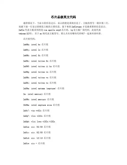
芯片组代码:2a69k:intel bx 芯片组2a69j:intel lx 芯片组2a69h: intel fx 芯片组2a59c: intel triton fx 芯片组2a59f: intel triton ii hx 芯片组2a59g: intel triton vx 芯片组2a59h: intel triton vx 芯片组2a59i: intel triton tx 芯片组2a59a: intel natoma (neptune) 芯片组2a: intel mercury 芯片组2a59b: intel mercury 芯片组2b59a: intel neptune eisa 芯片组2a5c7: via vt82c 芯片组2a5g7: vlsi vl82c 芯片组2a5gb: vlsi lynx vl82c/vl82c2a5ia: sis /02/03 芯片组2a5ic: sis /02/03 芯片组2a5id: sis /12/13 芯片组2a5ie: sis - 芯片组2a5if: sis 芯片组2a5ih: sis 芯片组2a5ii: sis 芯片组2a5ik: sis 芯片组2a5kb: ali /61/51 芯片组2a5kc: 目前未明2a5kf: ali /23 芯片组2a5ki: ali iv+ m/m 芯片组 (super tx 芯片组)2a5la: via apollo vp1 芯片组 (vt82cvp) ( vxpro 芯片组)2a5lc: via apollo vp2 芯片组 (amd 芯片组) 2a5ld: via vpx 芯片组 ( vxpro+ 芯片组) 2a5le: via apollo (m)vp32a5l7: via vt82c 2a5l9: via vt82cm2a5r5: forex a- 芯片组2a5ui: opti 82c// 芯片组2a5ul: opti 82c// 芯片组2a5um: opti 82c// 芯片组2a5un: optiviper-m82c//|viper 82c//芯片组2a5x7: umc 82c 芯片组2a5x8: umc umbf/umbf/umbf 芯片组2a4h2: contaq 82c-9 芯片组2a4ib: sis / 芯片组2a4kc: ali /45/31 芯片组2a4kd: ali 芯片组2a4l4: via a// 芯片组2a4l6: via // 芯片组2a4uk: opti-g- 芯片组2a4x5: umc / 芯片组2c: efar ecg-b 芯片组2c4i8: sis b/e 芯片组2c4i9: sis 85cb/e/g 芯片组2c4k9: ali 芯片组2c4j6: 目前未知2c4l2: via 82ca 芯片组2c4l6: via vtg 芯片组2c4uk: opti - g2c4x2: umc um82c/82c 芯片组2c4x6: umc umf/f2a: cyrix 芯片组 (mediagx)厂商代码:a0 asus(华硕)a1 abit(silicon star)(升技)a2 atrend (中凌)a3 asi (aquarius systems inc.) a7 arima twn ab aopen (建基) ad amaquestam mirageb0 biostar (映泰)b3 bcmc1 clevoc2 chiconyc3 chaintech (承启)c5 chapletc9 computrendcf flagpointd0 dataexpert (联讯)d1 dtk (创宏)d2 digital (dec)d3 digicomd4 dfi(钻石)e1 ecs (elitegroup) (磐英)e3 efae4 espcoe6 elonexec enpcf0 fic (fica) (大众)f2 free techf3 full yes (福扬)f5 fugutechf9 fordlianfd dataexpert or atima or gct (联讯) fh amptronfn amptrong0 giga-byte(技嘉)g3 gemlightg9 global circuit technologyh0 hsin-techh2 holco (shuttle)i3 iwill (艾威)i4 inventai5 informtechj1 jetway (jetboard, acorp) (捷波)j2 jamiconj3 j-bond(捷波)j4 jetta j6 jossk0 kapokk1 kameil1 lucky starm0 matram2 mycomp (tmc) and megastar (皇朝/麦肯) m3 mitacm4 micro-star(微星)m8 mustekm9 mlen5 nec o0 ocean (octek)(海洋)p1 pc-chips (明致)p4 asus(华硕)p8 azzap9 powertechpa epox (pronix) (磐英)pc pineq0 quanta (twn)q1 qdi(联想)r0 mtech (rise)r2 rectrons2 soyo (梅捷)s5 shuttle (holco)s9 spring circlesa seanixsc sukjung (auhua electronics co. ltd.)se smt (sundance multiprocessor technology ltd) sh sye (shing yunn technology co., ltd.)sm san-li and hope vision sn soltek (硕泰克)t0 twinhead(伦飞)t1 taemung or fentecht4 takent5 tyant6 trigentb totemtg tekram(建邦)tj totemtp commate, ozzou0 u-boardu2 air (uhc)u6 unitronv3 vtech (pcpartner)v5 vision top technologyv6 vobisv7 ykm (distribution by dayton micron)w0 wintec (edom)z1 zida (tomato boards)补足:主板购买注意事项1、工作稳定,兼容性好。
Richtek技术有限公司RT8525GS产品说明书
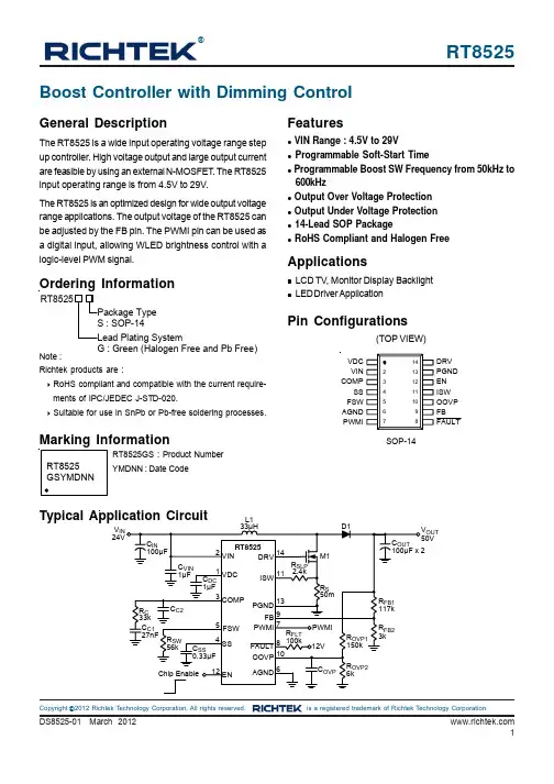
RT8525®DS8525-01 March 20121©Copyright 2012 Richtek Technology Corporation. All rights reserved. is a registered trademark of Richtek Technology Corporation.Ordering InformationNote :Richtek products are :` RoHS compliant and compatible with the current require-ments of IPC/JEDEC J-STD-020.` Suitable for use in SnPb or Pb-free soldering processes.Boost Controller with Dimming ControlPin ConfigurationsSOP-14(TOP VIEW)RT8525GS : Product NumberYMDNN : Date CodeGeneral DescriptionThe RT8525 is a wide input operating voltage range step up controller. High voltage output and large output current are feasible by using an external N-MOSFET . The RT8525input operating range is from 4.5V to 29V.The RT8525 is an optimized design for wide output voltage range applications. The output voltage of the RT8525 can be adjusted by the FB pin. The PWMI pin can be used as a digital input, allowing WLED brightness control with a logic-level PWM signal.FeatureszVIN Range : 4.5V to 29VzProgrammable Soft-Start Timez Programmable Boost SW Frequency from 50kHz to 600kHzz Output Over Voltage Protection z Output Under Voltage Protection z 14-Lead SOP Packagez RoHS Compliant and Halogen FreeApplicationszLCD TV, Monitor Display Backlight zLED Driver ApplicationDRV PGND ISW EN OOVP FB FAULTVDC VIN COMPSS FSW AGND PWMITypical Application CircuitG : Green (Halogen Free and Pb Free)L1V OUT2RT8525DS8525-01 March 2012©Copyright 2012 Richtek Technology Corporation. All rights reserved. is a registered trademark of Richtek Technology Corporation.Function Block Diagram3RT8525DS8525-01 March 2012©Copyright 2012 Richtek Technology Corporation. All rights reserved. is a registered trademark of Richtek Technology Corporation.Electrical Characteristics(V IN = 21V, V OUT = 50V, T A = 25°C, unless otherwise specified)Absolute Maximum Ratings (Note 1)z VIN to GND ------------------------------------------------------------------------------------------------------------------ −0.3V to 32V z VDC, DRV, FAULT to GND----------------------------------------------------------------------------------------------- −0.3V to 13.2V z EN, COMP , SS, FSW, FB, OOVP , ISW, PWMI to GND --------------------------------------------------------- −0.3V to 6V zPower Dissipation, P D @ T A = 25°CSOP-14----------------------------------------------------------------------------------------------------------------------1.000W zPackage Thermal Resistance (Note 2)SOP-14 , θJA ----------------------------------------------------------------------------------------------------------------100°C/W z Lead Temperature (Soldering, 10 sec.)-------------------------------------------------------------------------------260°C z Junction T emperature -----------------------------------------------------------------------------------------------------150°Cz Storage T emperature Range -------------------------------------------------------------------------------------------- −65°C to 150°C zESD Susceptibility (Note 3)HBM --------------------------------------------------------------------------------------------------------------------------2kV MM ----------------------------------------------------------------------------------------------------------------------------200VRecommended Operating Conditions (Note 4)z Supply Input Voltage, VIN -----------------------------------------------------------------------------------------------4.5V to 29V z Junction T emperature Range -------------------------------------------------------------------------------------------- −40°C to 125°C zAmbient T emperature Range -------------------------------------------------------------------------------------------- −40°C to 85°C4RT8525DS8525-01 March 2012©Copyright 2012 Richtek Technology Corporation. All rights reserved. is a registered trademark of Richtek Technology Corporation.Note 1. Stresses beyond those listed “Absolute Maximum Ratings ” may cause permanent damage to the device. These arestress ratings only, and functional operation of the device at these or any other conditions beyond those indicated in the operational sections of the specifications is not implied. Exposure to absolute maximum rating conditions may affect device reliability.Note 2. θJA is measured at T A = 25°C on a low effective thermal conductivity single-layer test board per JEDEC 51-3.Note 3. Devices are ESD sensitive. Handling precaution is recommended.Note 4. The device is not guaranteed to function outside its operating conditions..RT8525Copyright 2012 Richtek Technology Corporation. All rights reserved. is a registered trademark of Richtek Technology Corporation.Feedback Voltage vs. Temperature1.01.11.21.31.41.5-50-25255075100125Temperature (°C)F e e d b a c k V o l t a g e(V )Feedback Voltage vs. Input Voltage1.01.11.21.31.41.54914192429Input Voltage (V)F e e d b a c k V o l t a g e (V )Typical Operating CharacteristicsBoost Efficiency vs. Load CurrentSwitching Frequency vs. TemperatureQuiescent Current vs. Input Voltage0.00.51.01.52.02.53.04914192429Input Voltage (V) Q u i e s c e n t C u r r e n t (m A )Quiescent Current vs. Temperature0.00.51.01.52.02.53.0-50-25255075100125Temperature (°C)Q u i e s c e n t C u r r e n t (m A )6RT8525DS8525-01 March 2012©Copyright 2012 Richtek Technology Corporation. All rights reserved. is a registered trademark of Richtek Technology Corporation.Applications InformationThe RT8525 is a wide input operating voltage range step up controller. High voltage output and large output current are feasible by using an external N-MOSFET. The protection functions include output over voltage, output under voltage, over temperature and current limiting protection.Boost Output Voltage SettingThe regulated output voltage is set by an external resistor divider according to the following equation :⎛⎞×⎜⎟⎝⎠FB1OUT FB FB FB2R V = V 1+, where V = 1.25V (typ.)R The recommended value of R FB2 should be at least 1k Ωfor saving sacrificing. Moreover, placing the resistor divider as close as possible to the chip can reduce noise sensitivity.Boost Switching FrequencyThe RT8525 boost driver switching frequency is able to be adjusted by a resistor R SW ranging from 18k Ω to 220k Ω. The following figure illustrates the corresponding switching frequency within the resistor range.Figure 1. Boost Switching FrequencySwitching Frequency vs. R SW0100200300400500600050100150200250R SW (k ) f S W (k H z )ΩBoost Loop CompensationThe voltage feedback loop can be compensated by anexternal compensation network consisted of R C , C C1 and C C2. Choose R C to set high frequency gain for fast transient response. Select C C1 and C C2 to set the zero and pole to maintain loop stability. For typical application,V IN = 24V, V OUT = 50V, C OUT = 100μF x 2, L1 = 33μH,while the recommended value for compensation is as follows : R C = 33k Ω, C C1 = 27nF.Soft-StartThe soft-start of the RT8525 can be achieved by connecting a capacitor from the SS pin to GND. The built-in soft-start circuit reduces the start-up current spike and output voltage overshoot. The external capacitor charged by an internal 4μA constant charging current determines the soft-start time. The SS pin limits the rising rate of the COMP pin voltage and thereby limits the peak switch current.The soft-start interval is set by the soft-start capacitor according to the following equation :≅××5SS SS t C 510A typical value for the soft-start capacitor is 0.33μF. The soft-start capacitor is discharged when EN voltage falls below its threshold after shutdown delay or UVLO occurs.Slope Compensation and Current LimitingA slope compensation is applied to avoid sub-harmonic oscillation in current-mode control. The slope compensation voltage is generated by the internal ramp current flow through a slope compensation resistor R SLP .The inductor current is sensed by the sensing resistor R S . Both of them are added and presented on the ISW pin. The internal ramp current is rising linearly form zero at the beginning of each switching cycle to 50μA in maximum on-time of each cycle. The slope compensation resistor R SLP can be calculated by the following equation :where R S is current sensing resistor, L is inductor value,and f SW is boost switching frequency.The current flow through inductor during charging period is detected by a sensing resistor R S . Besides, the slope compensation voltage also attributes magnitude to ISW.As the voltage at the ISW pin is over 0.4V, the DRV will be pulled low and turn off the external N-MOSFET. So that the inductor will be forced to leave charging stage and enter discharging stage to prevent over current. The current limiting can be calculated by the following equation:()−××××OUT IN SSLP SW V V R R >2L 50μf7RT8525DS8525-01 March 2012©Copyright 2012 Richtek Technology Corporation. All rights reserved. is a registered trademark of Richtek Technology Corporation.where I L, PK is peak inductor current, and D MAX is maximum duty.Output Over Voltage ProtectionThe output voltage can be clamped at the voltage level determined by the following equation :⎛⎞×⎜⎟⎝⎠OVP1OUT (OOVP)OOVP OVP2OOVP R V = V 1+,R where V = 2.5V (typ.)Power MOSFET SelectionFor the applications operating at high output voltage,switching losses dominate the overall power loss.Therefore, the power N-MOSFET switch is typically chosen for drain voltage, VDS, rating and low gate charge.Consideration of switch on-resistance R DS(ON) is usually secondary. The VDC regulator in the RT8525 has a fixed output current limit to protect the IC and provide 12V DRV voltage for N-MOSFET switch gate driver.()×−×××2OUT SW OUTD 1D V L =2f I Inductor SelectionThe boundary value of the inductance L between Discontinuous Conduction Mode (DCM) and Continuous Conduction Mode (CCM) can be approximated by the following equation :Figure 2. Fault Protection Function BlockwhereV OUT is the maximum output voltage,V IN is the minimum input voltage,fsw is the operating frequency,I OUT is the sum of current from all LED strings,and D is the duty cycle calculated by the following equation :−OUTIN OUTV V D = V The boost converter operates in DCM over the entire input voltage range if the inductor value is less than the boundary value L. With an inductance greater than L, the converter operates in CCM at the minimum input voltage and may transit to DCM at higher voltages. The inductor must be−××MAX SLP S L, PK0.4D R 50μR <I be under 0.25V. Then the protection function will perform action 2 to turn off the driver. When protection function is released, the RT8525 will re-start.On the other hand, if the triggered protection is OOVP ,the voltage at node A will be decided by voltage divider composed of R FLT and the internal 8k Ω resistor. This voltage must be designed between 0.25V and 1.25V by choosing R FLT appropriately. Once the OOVP turns on the Switch 2, the divided FAULT voltage will activate action 1to turn off the driver without resetting soft-start. Therefore,when protection function OOVP is released, the RT8525will be in normal operation.where R OVP1 and R OVP2 are the voltage divider connected to the OOVP pin.Fault ProtectionThe FAULT pin will be pulled low once a protection is triggered, and a suitable pulled-high R FLT is required. The suggested R FLT is 100k Ω if the pulled-high voltage was 12V. The following figure illustrates the fault protection function block. If one of the OUVP and OTP occurs, the switch 1 will be turned on, and the voltage at node A will8RT8525DS8525-01 March 2012©Copyright 2012 Richtek Technology Corporation. All rights reserved. is a registered trademark of Richtek Technology Corporation.Thermal ConsiderationsFor continuous operation, do not exceed absolute maximum junction temperature. The maximum power dissipation depends on the thermal resistance of the IC package, PCB layout, rate of surrounding airflow, and difference between junction and ambient temperature. The maximum power dissipation can be calculated by the following formula :P D(MAX) = (T J(MAX) − T A ) / θJAwhere T J(MAX) is the maximum junction temperature, T A is the ambient temperature, and θJA is the junction to ambient thermal resistance.For recommended operating condition specifications, the maximum junction temperature is 125°C. The junction to ambient thermal resistance, θJA , is layout dependent. For SOP-14 packages, the thermal resistance, θJA , is 100°C/W on a standard JEDEC 51-3 single-layer thermal test board. The maximum power dissipation at T A = 25°C can be calculated by the following formula :P D(MAX) = (125°C − 25°C) / (100°C/W) = 1.000W for SOP-14 packageThe maximum power dissipation depends on the operating ambient temperature for fixed T J(MAX) and thermal resistance, θJA . The derating curve in Figure 4 allows the designer to see the effect of rising ambient temperature on the maximum power dissipation.×××+××ηOUT OUT LPK INV I VIN D TI = V 2L where η is the efficiency of the power converter.⎡⎤⎛⎞⎛⎞×+Δ−+−Δ−×⎜⎟⎜⎟⎢⎥⎝⎠⎝⎠⎣⎦××ΔININ L OUT IN L OUT OUT OUT OUT1SWV 111Q = I I I I I I 222V 1 = C V f where f SW is the switching frequency, and ΔI L is the inductor ripple current. Move C OUT to the left side to estimate the value of ΔV OUT1 as the following equation :×Δ××ηOUTOUT1OUT SWD I V =C f Finally, by taking ESR into consideration, the overall output ripple voltage can be determined as the following equation :×Δ×+××OUTOUT IN OUT SWD I V = I ESR ηC f Figure 3. The Output Ripple Voltage without theContribution of ESR Diode SelectionSchottky diodes are recommended for most applicationsbecause of their fast recovery time and low forward voltage.The power dissipation, reverse voltage rating and pulsating peak current are the important parameters for Schottky diode selection. Make sure that the diode's peak current rating exceeds I LPK , and reverse voltage rating exceeds the maximum output voltage.Capacitor SelectionOutput ripple voltage is an important index for estimating the performance. This portion consists of two parts, one is the product of input current and ESR of output capacitor,another part is formed by charging and discharging process of output capacitor. Refer to figure 3, evaluate ΔV OUT1 by ideal energy equalization. According to the definition of Q, the Q value can be calculated as following equation :selected with a saturated current rating greater than the peak current provided by the following equation :9RT8525DS8525-01 March 2012©Copyright 2012 Richtek Technology Corporation. All rights reserved. is a registered trademark of Richtek Technology yout ConsiderationsPCB layout is very important for designing switching powerconverter circuits. The following layout guides should be strictly followed for best performance of the RT8525.`The power components L 1, D 1, C IN , C OUT , M 1 and R S must be placed as close as possible to reduce current loop. The PCB trace between power components must be as short and wide as possible.`Place components R FB1, R FB2, R OVP1 and R OVP2 close to IC as possible. The trace should be kept away from the power loops and shielded with a ground trace to prevent any noise coupling.`The compensation circuit should be kept away from the power loops and should be shielded with a ground trace to prevent any noise coupling. Place the compensation components to the COMP pin as close as possible, no matter the compensation is R C , C C1 or C C2.Figure 5. PCB Layout GuideFigure 4. Derating Curve of Maximum Power DissipationPlace the power components as close as possible. The traces feedback pin. The divider center trace must beshorter and avoid the trace near any switching nodes.S for better stability.0.00.10.20.30.40.50.60.70.80.91.01.1255075100125Ambient Temperature (°C)M a x i m u m P o w e r D i s s i p a t i o n (W )10RT8525DS8525-01 March 2012Richtek Technology Corporation5F, No. 20, Taiyuen Street, Chupei City Hsinchu, Taiwan, R.O.C.Tel: (8863)5526789Richtek products are sold by description only. Richtek reserves the right to change the circuitry and/or specifications without notice at any time. Customers shouldobtain the latest relevant information and data sheets before placing orders and should verify that such information is current and complete. Richtek cannot assume responsibility for use of any circuitry other than circuitry entirely embodied in a Richtek product. Information furnished by Richtek is believed to be accurate and reliable. However, no responsibility is assumed by Richtek or its subsidiaries for its use; nor for any infringements of patents or other rights of third parties which may result from its use. No license is granted by implication or otherwise under any patent or patent rights of Richtek or its subsidiaries.Outline DimensionM14–Lead SOP Plastic Package。
Silver Telecom 2022 EvalAg7x61 单通道 PSE 增益转换器 评估板
V1.0 February 2022Evaluation Board User ManualEvaluation BoardUser ManualSilvertelEvalAg7x61 Evaluation Board User ManualVersion 1.0 – February 2022Table of Contents1Kit Contents (3)2Additional Components (3)3Board Layout (3)Link Settings (3)4Introduction (4)5Input (4)Supply (4)DC/DC Adjust (4)Data (4)6Auxiliary Supply (5)7PSE Output (5)Power option select (5)Pairset Select (5)Operation (6)Status Output (6)8Test Setup (7)9Additional information (7)10Schematic (8)11Bill of Materials (9)Table of FiguresFigure 1: EvalAg6120 Board Layout (3)Figure 2: Basic Test Setup (7)1 Kit Contents➢EvalAg6120 Evaluation Board2 Additional Components➢Ag6120 PSE Module➢Ag7100 or Ag7200 Isolated Boost Converter Module3 Board LayoutFigure 1: EvalAg6120 Board Layout Link SettingsLK1-4 – Output Pairset EnableLK5 – Status LED EnableLK6 – Output Power SelectLK7&8 – DC/DC AdjustLK9 – PoE Power LED EnableLK10 – DC/DC Converter Power LED Enable4 IntroductionThis Manual is a guide to using the EvalAg7x61 evaluation board which can be fitted with a Silvertel Ag6120 Single Channel Power Sourcing Equipment (PSE) module along with either a Silvertel Ag7200 or Ag7100 isolated boost converter module for a single port PSE powered via 5V-15V for Type 1 applications or 12V-27V for Type 2 applications.This board is designed to assist with evaluating the use of Silvertel's Ag6120 in conjunction with one of Silvertel's isolated boost modules in an application; as such it has been designed to pass through 10/100/1000/10GBASE-T Ethernet data signals from any source connected to J100 onto the powered device connected to J101This Evaluation board can also be used with the Ag6100 or Ag6110 PSE Modules; however, the output power settings, set by LK6, are not a feature of those modules.5 InputSupplyThe EvalAg7x61 evaluation board is powered using a DC Power supply connected to either J3 or J1 and 2. This supply should deliver either 5V-15V or 12V-27V depending on the model of boost converter fitted.For Type 1 (IEEE802.3af) applications the EvalAg7x61 can be fitted with an Ag7200 isolated boost converter for a maximum power output of 20W. With the Ag7200 fitted the EvalAg7x61 should be supplied with a DC Power supply of 5V-15VFor Type 2 (IEEE802.3at) applications the EvalAg7x61 can be fitted with an Ag7100 isolated boost converter for a maximum power output of 40W. With the Ag7100 fitted the EvalAg7x61 should be supplied with a DC Power supply of 12V-27VAdditionally, the EvalAg7x61 can be supplied from an auxiliary DC Power supply delivering between 44V and 57V to J4.Both DC jack connectors J3 and J4 are configured with the positive supply connected to the centre pin and 0V to the outer ring.DC/DC AdjustThe output voltage of the Boost module can be adjusted by moving the jumper on DC/DC Adjust headers between LK7 and LK8. Placing the Jumper on LK8 will result in the output of the DC/DC converter being set to 48V. Removing the jumper from LK8 and inserting it on LK7 will result in the DC/DC converter outputting 57V.If a different voltage is required, please contact Silvertel for more details.DataA data source can be connected to the Data port J100 via RJ45 connector. This data will be transposed onto the Data and Power output port J101 via the data transformer. The data traces on the evaluation board have been designed to pass through10/100/1000/10GBASE-T Ethernet data signals. No processing or amplification of this signal will be performed on the evaluation board6 Auxiliary SupplyThe Auxiliary supply port, J4, can be used to either inject a secondary supply for theAg6120 or as an output so that the fitted DC/DC converter can be used to power external devices.If J4 is used as an output, it is important to remember that there is an OR-ing diode fitted to the EvalAg7x61, so there will be a voltage drop on the output of the Boost converter.7 PSE OutputPower option selectThe Ag6120 has an option to select its output power and class. These can be chosen by placing a jumper on the appropriate pins of LK6. The power option select should be set while the Ag6120 is powered off, if the power option is changed while the device is powered, the change will not occur until after the Ag6120 output has been power cycled.Mode Classificationtype*2Maxoutputpower*3Connectedpair sets*4Legacy Type 2 (at)*1 IEEE802.3at 38W Either 2Type 1 (af) IEEE802.3bt 20W Either 2Type 2 (at) IEEE802.3bt 38W Either 2 Legacy high power at + legacy class 5 75W All 4BT 1 pair (bt class 5)*5 IEEE802.3bt 46W Either 2/all 4BT Type 3 (bt class 6)*5IEEE802.3bt 75W All 4Table 1: option selections and limits*1 Not recommend for new designs only for use as drop in replacement of the Ag6100*2 See section 5.5.2: Classification of the Ag6120 Datasheet for details*3 See sections 5.7: Output Current Limits & 5.8: Output Power of the Ag6120 Datasheet for details*4 See section 5.4: Port Output of the Ag6120 Datasheet for details*5 Compatible with IEEE802.3bt single signature PDsPairset SelectThe EvalAg7x61 contains four links LK1-4 that connect the pairsets to the outputs of the Ag6120. In order to enable power transfer down a given pairset a jumper should be inserted onto the relevant link or removed if power is not desired down that given pairset. Pairsets 1-2 and 4-5 are connected to the positive output of the Ag6120. While pairsets 3-6 and 7-8 are connected to the negative output of the Ag6120. In high power modes all four jumpers should be fitted.When only two pairsets are to be connected, in order to guarantee operation either pairsets 1-2 & 3-6 should be connected or pairsets 4-5 & 7-8 should be connected.OperationTo ensure that the Ag6120 does not apply power to a non-PoE enabled device the output port first checks for a valid PoE signature. If the Ag6120 does not see a valid signature then it will disconnect, wait approximately 2 seconds then try again. Once a valid signature has been detected the Ag6120 will then perform classification to determine the power requirement of the PD, only after this has occurred will the Ag6120 supply power to the powered device.Status OutputThe Status LED will illuminate if the Ag6120 is providing power to the output port. It will also flash as per the table below when an error has occurred. If this functionality is not desired, it can be disabled by removing the jumper on link LK5.Fault Condition Status Pulses (200ms)Short Circuit 1 x FlashOver Current 2 x FlashesSignature/Class Error 3 x FlashesInput Voltage < UVLO limit 4 x FlashesTable 2: Status Output8 Test SetupFigure 2 shows the basic set up using the EvalAg7x61 evaluation board fitted with anAg6120 and Ag7100 for a Type 2 PSE setup capable of supplying the application with up to 40W of power. This setup is powered using a 12V DC power supply capable of supplying up to 4A to full power output is available.The power option select and Pairset links should already be set before supplying power to the evaluation board. The powered device and data source need not be connected before power is applied.The equipment required: -➢Power supply unit, 5V-27V output e.g. 30V bench power supply➢Powered device➢CAT5e/CAT6a cablesOptional equipment: -➢Data source e.g. PCFigure 2: Basic Test Setup9 Additional informationFull operating conditions and feature set can be found in the Ag6120, Ag7100 and Ag7200 product datasheets, available from .10 Schematic11 Bill of Materials。
74LVC1G14单芯片阈值稳定器反转器数据表说明书
74LVC1G14Single Schmitt-trigger inverterRev. 15 — 8 June 2018Product data sheet1General descriptionThe 74LVC1G14 provides the inverting buffer function with Schmitt-trigger input. It iscapable of transforming slowly changing input signals into sharply defined, jitter-freeoutput signals.The input can be driven from either 3.3 V or 5 V devices. This feature allows the useof this device in a mixed 3.3 V and 5 V environment. Schmitt-trigger action at the inputmakes the circuit tolerant for slower input rise and fall time.This device is fully specified for partial power-down applications using I OFF. The I OFFcircuitry disables the output, preventing the damaging backflow current through thedevice when it is powered down.2Features and benefits•Wide supply voltage range from 1.65 V to 5.5 V•High noise immunity•Complies with JEDEC standard:–JESD8-7 (1.65 V to 1.95 V)–JESD8-5 (2.3 V to 2.7 V)–JESD8-B/JESD36 (2.7 V to 3.6 V).•±24 mA output drive (V CC = 3.0 V)•CMOS low power consumption•Latch-up performance exceeds 250 mA•Direct interface with TTL levels•Unlimited rise and fall times•Input accepts voltages up to 5 V•Multiple package options•ESD protection:–HBM: ANSI/ESDA/JEDEC JS-001 Class 2 exceeds 2000 V–MM: JESD22-A115-A exceeds 200 V.•Specified from -40 °C to +85 °C and -40 °C to +125 °C.3Applications•Wave and pulse shaper•Astable multivibrator•Monostable multivibratorSingle Schmitt-trigger inverter 4Ordering information5Marking[1]The pin 1 indicator is located on the lower left corner of the device, below the marking code.Single Schmitt-trigger inverter6Functional diagram7Pinning information7.1Pinning74LVC1G14n.c.V CCA GNDY001aab65512354Figure 4. Pin configuration SOT353-1 and SOT75374LVC1G14A 001aae976n.c.GNDn.c.V CC YT ransparent top view231546Figure 5. Pin configuration SOT886, SOT891, SOT1115and SOT1202n.c.V CCGND13254AY aaa-003024Transparent top view 74LVC1G14Figure 6. Pin configuration SOT1226 (X2SON5)aaa-028401Transparent top view74LVC1G14V CC4Y3A 1GND 2Figure 7. Pin configuration SOT1269-2 (X2SON4)7.2Pin descriptionSingle Schmitt-trigger inverter8Functional description[1][1]H = HIGH voltage level; L = LOW voltage level9Limiting valuesTable 5. Limiting valuesIn accordance with the Absolute Maximum Rating System (IEC 60134). Voltages are referenced to GND (ground = 0 V).[1]The input and output voltage ratings may be exceeded if the input and output current ratings are observed.[2]For TSSOP5 and SC-74A packages: above 87.5 °C the value of P tot derates linearly with 4.0 mW/K.For XSON6 and X2SON5 package: above 118 °C the value of P tot derates linearly with 7.8 mW/K.[3]For X2SON4 packages: above 57 °C the value of P tot derates linearly with 1.7 mW/K.Single Schmitt-trigger inverter 10Recommended operating conditions11Static characteristicsTable 7. Static characteristicsAt recommended operating conditions; voltages are referenced to GND (ground = 0 V).Single Schmitt-trigger inverter[1]All typical values are measured at maximum V CC and T amb = 25 °C.Table 8. Transfer characteristicsVoltages are referenced to GND (ground = 0 V); for test circuit see Figure 9.[1]Typical values are measured at T amb = 25 °C and V CC = 1.8 V, 2.5 V, 2.7 V, 3.3 V and 5.0 V respectively.Single Schmitt-trigger inverter 12Dynamic characteristicsTable 9. Dynamic characteristicsVoltages are referenced to GND (ground = 0 V); for test circuit see Figure 9.[1]Typical values are measured at T amb = 25 °C and V CC = 1.8 V, 2.5 V, 2.7 V, 3.3 V and 5.0 V respectively.[2]t pd is the same as t PLH and t PHL.[3]C PD is used to determine the dynamic power dissipation (P D in μW).P D = C PD x V CC2 x f i + (C L x V CC2 x f o) where:f i = input frequency in MHz;f o = output frequency in MHz;C L = output load capacitance in pF;V CC = supply voltage in V.12.1Waveform and test circuitSingle Schmitt-trigger inverterSingle Schmitt-trigger inverter12.2Waveforms transfer characteristics13Application informationThe slow input rise and fall times cause additional power dissipation, this can becalculated using the following formula:P add = f i x (t r x ΔI CC(AV) + t f x ΔI CC(AV)) x V CC where:•P add = additional power dissipation (μW);•f i = input frequency (MHz);•t r = input rise time (ns); 10 % to 90 %;•t f = input fall time (ns); 90 % to 10 %;•ΔI CC(AV) = average additional supply current (μA).Average ΔI CC(AV) differs with positive or negative input transitions, as shown in Figure 13.An example of a relaxation circuit using the 74LVC1G14 is shown in Figure 14.Single Schmitt-trigger inverteraaa-0219851234560.20.40.60.811.2V CC (V)KFigure 15. Typical K-factor for relaxation oscillatorSingle Schmitt-trigger inverter 14Package outlineSingle Schmitt-trigger inverterSingle Schmitt-trigger inverterSingle Schmitt-trigger inverterSingle Schmitt-trigger inverterSingle Schmitt-trigger inverterSingle Schmitt-trigger inverterSingle Schmitt-trigger inverterSingle Schmitt-trigger inverter 15Abbreviations16Revision historySingle Schmitt-trigger inverter 17Legal information17.1 Data sheet status[1]Please consult the most recently issued document before initiating or completing a design.[2]The term 'short data sheet' is explained in section "Definitions".[3]The product status of device(s) described in this document may have changed since this document was published and may differ in case of multipledevices. The latest product status information is available on the Internet at URL .17.2 DefinitionsDraft — The document is a draft version only. The content is still under internal review and subject to formal approval, which may result in modifications or additions. Nexperia does not give any representations or warranties as to the accuracy or completeness of information included herein and shall have no liability for the consequences of use of such information.Short data sheet — A short data sheet is an extract from a full data sheet with the same product type number(s) and title. A short data sheet is intended for quick reference only and should not be relied upon to contain detailed and full information. For detailed and full information see the relevant full data sheet, which is available on request via the local Nexperia sales office. In case of any inconsistency or conflict with the short data sheet, the full data sheet shall prevail.Product specification — The information and data provided in a Product data sheet shall define the specification of the product as agreed between Nexperia and its customer, unless Nexperia and customer have explicitly agreed otherwise in writing. In no event however, shall an agreement be valid in which the Nexperia product is deemed to offer functions and qualities beyond those described in the Product data sheet.17.3 DisclaimersLimited warranty and liability — Information in this document is believed to be accurate and reliable. However, Nexperia does not give any representations or warranties, expressed or implied, as to the accuracyor completeness of such information and shall have no liability for the consequences of use of such information. Nexperia takes no responsibility for the content in this document if provided by an information source outside of Nexperia. In no event shall Nexperia be liable for any indirect, incidental, punitive, special or consequential damages (including - without limitation -lost profits, lost savings, business interruption, costs related to the removal or replacement of any products or rework charges) whether or not such damages are based on tort (including negligence), warranty, breach of contract or any other legal theory. Notwithstanding any damages that customer might incur for any reason whatsoever, Nexperia's aggregate and cumulative liability towards customer for the products described herein shall be limited in accordance with the Terms and conditions of commercial sale of Nexperia.Right to make changes — Nexperia reserves the right to make changesto information published in this document, including without limitation specifications and product descriptions, at any time and without notice. This document supersedes and replaces all information supplied prior to the publication hereof.Suitability for use — Nexperia products are not designed, authorized or warranted to be suitable for use in life support, life-critical or safety-critical systems or equipment, nor in applications where failure or malfunctionof an Nexperia product can reasonably be expected to result in personal injury, death or severe property or environmental damage. Nexperia and its suppliers accept no liability for inclusion and/or use of Nexperia products in such equipment or applications and therefore such inclusion and/or use is at the customer’s own risk.Applications — Applications that are described herein for any of these products are for illustrative purposes only. Nexperia makes no representation or warranty that such applications will be suitable for the specified use without further testing or modification. Customers are responsible for the design and operation of their applications and products using Nexperia products, and Nexperia accepts no liability for any assistance with applications or customer product design. It is customer’s sole responsibility to determine whether the Nexperia product is suitable and fit for the customer’s applications and products planned, as well as for the planned application and use of customer’s third party customer(s). Customers should provide appropriate design and operating safeguards to minimize the risks associated with their applications and products. Nexperia does not accept any liability related to any default, damage, costs or problem which is based on any weakness or default in the customer’s applications or products, or the application or use by customer’s third party customer(s). Customer is responsible for doing all necessary testing for the customer’s applications and products using Nexperia products in order to avoid a default of the applications and the products or of the application or use by customer’s third party customer(s). Nexperia does not accept any liability in this respect.Limiting values — Stress above one or more limiting values (as defined in the Absolute Maximum Ratings System of IEC 60134) will cause permanent damage to the device. Limiting values are stress ratings only and (proper) operation of the device at these or any other conditions above thosegiven in the Recommended operating conditions section (if present) or the Characteristics sections of this document is not warranted. Constant or repeated exposure to limiting values will permanently and irreversibly affect the quality and reliability of the device.Terms and conditions of commercial sale — Nexperia products aresold subject to the general terms and conditions of commercial sale, as published at /profile/terms, unless otherwise agreed in a valid written individual agreement. In case an individual agreement is concluded only the terms and conditions of the respective agreement shall apply. Nexperia hereby expressly objects to applying the customer’s general terms and conditions with regard to the purchase of Nexperia products by customer.No offer to sell or license — Nothing in this document may be interpreted or construed as an offer to sell products that is open for acceptance orthe grant, conveyance or implication of any license under any copyrights, patents or other industrial or intellectual property rights.Export control — This document as well as the item(s) described herein may be subject to export control regulations. Export might require a prior authorization from competent authorities.Single Schmitt-trigger inverterNon-automotive qualified products — Unless this data sheet expressly states that this specific Nexperia product is automotive qualified, the product is not suitable for automotive use. It is neither qualified nor tested in accordance with automotive testing or application requirements. Nexperia accepts no liability for inclusion and/or use of non-automotive qualified products in automotive equipment or applications. In the event that customer uses the product for design-in and use in automotive applications to automotive specifications and standards, customer (a) shall use the product without Nexperia's warranty of the product for such automotive applications, use and specifications, and (b) whenever customer uses the product for automotive applications beyond Nexperia's specifications such use shall be solely at customer’s own risk, and (c) customer fully indemnifies Nexperia for any liability, damages or failed product claims resulting from customer design and use of the product for automotive applications beyond Nexperia's standard warranty and Nexperia's product specifications.Translations — A non-English (translated) version of a document is for reference only. The English version shall prevail in case of any discrepancy between the translated and English versions.17.4 TrademarksNotice: All referenced brands, product names, service names and trademarks are the property of their respective owners.74LVC1G14All information provided in this document is subject to legal disclaimers.© Nexperia B.V. 2018. All rights reserved. Product data sheet Rev. 15 — 8 June 201821 / 22Single Schmitt-trigger inverterContents1General description (1)2Features and benefits (1)3Applications (1)4Ordering information (2)5Marking (2)6Functional diagram (3)7Pinning information (3)7.1Pinning (3)7.2Pin description (3)8Functional description (4)9Limiting values (4)10Recommended operating conditions (5)11Static characteristics (5)12Dynamic characteristics (7)12.1Waveform and test circuit (7)12.2Waveforms transfer characteristics (9)13Application information (9)14Package outline (11)15Abbreviations (19)16Revision history (19)17Legal information (20)Please be aware that important notices concerning this document and the product(s)described herein, have been included in section 'Legal information'.© Nexperia B.V. 2018.All rights reserved.For more information, please visit: Forsalesofficeaddresses,pleasesendanemailto:***************************Date of release: 8 June 2018Document identifier: 74LVC1G14Mouser ElectronicsAuthorized DistributorClick to View Pricing, Inventory, Delivery & Lifecycle Information:N experia:74LVC1G14GS,13274LVC1G14GN,13274LVC1G14GF,13274LVC1G14GM,11574LVC1G14GM,132 74LVC1G14GV,12574LVC1G14GW,12574LVC1G14GX,12574LVC1G14GX4Z。
NXP i.MX 8M Plus Applications Processor Reference
Preview of i.MX 8M Plus Applications Processor Reference ManualGet entire reference manual (7406 pages, PDF)Document Number: IMX8MPRMRev. 1, 06/2021ContentsSection number Title PageChapter 1Introduction1.1Product Overview (9)1.2Target Applications (9)1.3Acronyms and Abbreviations (9)1.4Architectural Overview (12)Chapter 2Memory Map2.1Memory system overview (23)2.2Cortex-A53 Memory Map (24)2.3Cortex-M7 Memory Map (26)2.4DMA memory maps (29)2.5AIPS Memory Maps (30)2.6DAP Memory Map (36)2.7Audio Processor Memory Map (38)2.8HDMI_TX Subsystem Memory Map (38)Chapter 3Security3.1System Security (41)3.2Resource Domain Controller (RDC) (44)Chapter 4Arm Platform and Debug4.1Arm Cortex A53 Platform (A53) (91)4.2Arm Cortex M7 Platform (CM7) (97)4.3Messaging Unit (MU) (99)4.4Semaphore (SEMA4) (143)4.5On-Chip RAM Memory Controller (OCRAM) (161)4.6Network Interconnect Bus System (NIC) (164)4.7AHB to IP Bridge (AIPSTZ) (165)4.8Shared Peripheral Bus Arbiter (SPBA) (188)4.9TrustZone Address Space Controller (TZASC) (201)4.10System Debug (203)4.11System Counter (SYS_CTR) (207)Chapter 5Clocks and Power Management5.1Clock Control Module (CCM) (227)5.2General Power Controller (GPC) (566)5.3Crystal Oscillator (XTALOSC) (718)5.4Thermal Monitoring Unit (TMU) (722)Chapter 6SNVS, Reset, Fuse, and Boot6.1System Boot (741)6.2Fusemap (808)6.3On-Chip OTP Controller (OCOTP_CTRL) (824)6.4Secure Non-Volatile Storage (SNVS) (868)6.5System Reset Controller (SRC) (897)6.6Watchdog Timer (WDOG) (968)Chapter 7Interrupts and DMA7.1Interrupts and DMA Events (987)7.2Smart Direct Memory Access Controller (SDMA) (1008)7.3Enhanced Direct Memory Access (eDMA) (1256)7.4Interrupt Request Steering (IRQ_STEER) (1318)Chapter 8Chip IO and Pinmux8.1External Signals and Pin Multiplexing (1329)8.2IOMUX Controller (IOMUXC) (1352)8.3General Purpose Input/Output (GPIO) (1982)Chapter 9External Memory9.1External Memory Overview (2001)9.2DDR Controller (DDRC) (2003)9.3DDR BLK_CTRL (2164)9.4DDR PHY (DDR_PHY) (2166)9.5AHB-to-APBH Bridge with DMA (APBH-Bridge-DMA) (2177)9.662BIT Correcting ECC Accelerator (BCH) (2217)9.7General Purpose Media Interface (GPMI) (2280)Chapter 10Mass Storage10.1Enhanced Configurable SPI (ECSPI) (2339)10.2FlexSPI Controller (FlexSPI) (2369)10.3Ultra Secured Digital Host Controller (uSDHC) (2500)Chapter 11Connectivity11.1HSIO BLK_CTRL (2659)11.2Universal Serial Bus Controller (USB) (2680)11.3Universal Serial Bus PHY (USB_PHY) (2993)11.4PCI Express (PCIe) (2997)11.5PCI Express PHY (PCIe_PHY) (3369)11.6Ethernet MAC (ENET) (3754)11.7Ethernet Quality Of Service (ENET_QOS) (3957)11.8FlexCAN (4980)Chapter 12Timers12.1General Purpose Timer (GPT) (5123)12.2Pulse Width Modulation (PWM) (5142)Chapter 13Display, Imaging, and Camera13.1Display, Imaging, and Camera Overview (5155)13.2MEDIA BLK_CTRL (5163)13.3LCD Interface (LCDIF) (5233)13.4Image Sensing Interface (ISI) (5265)13.5MIPI CSI Host Controller (MIPI_CSI) (5347)13.6MIPI DSI Host Controller (MIPI_DSI) (5396)13.7MIPI D-PHY (MIPI_DPHY) (5469)13.8LVDS Display Bridge (LDB) (5493)13.9HDMI TX Controller (5496)13.10HDMI TX PHY (5779)13.11HDMI TX BLK_CTRL (5828)13.12HDMI TX Parallel Audio Interface (HTX_PAI) (5859)13.13HDMI TX Parallel Video Interface (HTX_PVI) (5871)13.14Image Signal Processor (ISP) (5895)13.15DeWarp (5901)13.16Machine Learning Neural Processing Unit (NPU) (5907)Chapter 14Audio14.1Audio Overview (5943)14.2AUDIO BLK_CTRL (5947)14.3PDM Microphone Interface (MICFIL) (5977)14.4Synchronous Audio Interface (SAI) (6023)14.5Asynchronous Sample Rate Converter (ASRC) (6077)14.6Enhanced Audio Return Channel (eARC) (6162)14.7Audio DSP (HiFi 4 DSP) (6231)Chapter 15Graphics Processing Unit (GPU)15.1GPU Overview (6239)15.22D Graphics Processing Unit (GPU2D) (6240)15.33D Graphics Processing Unit (GPU3D) (6254)Chapter 16Video Processing Unit (VPU)16.1VPU G1 Decoder (6263)16.2VPU G2 Decoder (6429)16.3VPU VC8000E Encoder (6665)16.4VPU BLK_CTRL (7256)Chapter 17Low Speed Communication and Interconnects17.1I2C Controller (I2C) (7269)17.2Universal Asynchronous Receiver/Transmitter (UART) (7293)Chapter 1Introduction1.1Product OverviewThis chapter introduces the architecture of the i.MX 8M Plus Applications Processor. The i.MX 8M Plus family is a set of NXP products focused on machine learning applications, combining state-of-art multimedia features with high-performance processing optimized for low-power consumption.The i.MX 8M Plus Applications Processor relies on a powerful fully coherent core complex based on a quad Cortex-A53 cluster, a Cortex-M7 coprocessor, audio digital signal processor, machine learning and graphics accelerators.The i.MX 8M Plus provides additional computing resources and peripherals:•Advanced security modules for secure boot, cipher acceleration and DRM support •A wide range of audio interfaces•Large set of peripherals that are commonly used in consumer/industrial markets including USB , PCIe, Ethernet, and CAN1.2Target ApplicationsThe i.MX 8M Plus Media Applications Processor targets applications on:•Smart Homes, Buildings and Cities•Machine Learning and Industrial Automation•Consumer and Pro Audio/Voice Systems1.3Acronyms and AbbreviationsThe table below contains acronyms and abbreviations used in this document.Acronyms and AbbreviationsAcronyms and Abbreviated TermsTerm Meaning ADC Analog-to-Digital ConverterAHB Advanced High-performance BusAIPS Arm IP BusALU Arithmetic Logic UnitAMBA Advanced Microcontroller Bus ArchitectureAPB Advanced Peripheral BusASRC Asynchronous Sample Rate ConverterAXI Advanced eXtensible InterfaceCA/CM Arm Cortex-A/Cortex-MCAAM Cryptographic Acceleration and Assurance Module CA53Arm Cortex A53 CoreCAN Controller Area NetworkCM7Arm Cortex M7 CoreCPU Central Processing UnitCSI CMOS Sensor InterfaceCSU Central Security UnitCTI Cross Trigger InterfaceD-cache Data cacheDAP Debug Access PortDDR Double data rateDMA Direct memory accessDPLL Digital phase-locked loopDRAM Dynamic random access memoryECC Error correcting codesECSPI Enhanced Configurable SPILPSPI Low-power SPIEDMA Enhanced Direct Memory AccessEIM External Interface ModuleENET EthernetEPIT Enhanced Periodic Interrupt TimerEPROM Erasable Programmable Read-Only MemoryETF Embedded Trace FIFOETM Embedded Trace MacrocellFIFO First-In-First-OutGIC General Interrupt ControllerGPC General Power ControllerGPIO General-Purpose I/OGPR General-Purpose RegisterGPS Global Positioning SystemTable continues on the next page...Continue Reading This Reference ManualGet entire reference manual (7406 pages, PDF)Stay informed when design resources related to this product are updated.Go to i.MX 8M Plusi.MX 8M Plus Applications Processor Reference Manual, Rev. 1, 06/202111NXP Semiconductors。
迪拜狗MINI NDI编码器和解码器用户指南(2018年12月)说明书

USER GUIDE | DECEMBER 2018MINIWELCOME TO THE FUTURE.4. GETTING TO KNOW MINIPhysical connectorsPowering Mini PoE (Power over Ethernet)DC/D-TapThermal management5.POWERING ON SEQUENCEIndication of system boot processOPERATING MINIWeb configuration panelAccess via web browser (URL)BirdDog Finder applicationAccessing Mini via an IP address Accessing Mini on a network without a DHCP server6.PASSWORD MANAGEMENTDefault passwordPassword resetCONFIGURING VIDEO INPUTSAutomatic input7.Semi-automatic inputManual input8.AUDIOEnabling or disabling AudioAudiosetup 8.NDI DECODE OPERATIONChanging modes from NDI Encoder to NDI Decoder Selecting an NDI source to decodeChanging back to NDI Encode operation 10.NETWORK SETTINGS AND DEVICE NAMING Device namingIP configuration methodDHCP IP addressStatic IP address11.TALLY SUPPORTOnboard TallyProgram TallyPreview TallyTally border overlay on loop12.FACTORY RESETSettings resetFIRMWARE UPDATE13.RECEIVING MINI STREAMSNewTek Studio MonitorNewTek TriCaster SeriesMINITHE WORLD’S SMALLEST NDI ENCODER AND DECODER.GETTING TO KNOW MINIThanks for purchasing BirdDog Mini. Please take some time to read this document to allow you to get the most out of your purchase and familiarize yourself with the features available in the unit.Physical connectors1. LED Indicator2. 1Gb Ethernet (Power over Ethernet)3. HDMI Input4. HDMI Output5. Audio Headset connector6. DC Input (5-18v DC)7. Reset SwitchPowering MiniMini is equipped with a sophisticated system allowing power from various sources:PoE (Power over Ethernet)PoE is a convenient way to power Mini as it allows both data and power to be sent through the same standard Ethernet cable. To take advantage of PoE, the network switch that Mini is directly plugged into must support PoE, in either 802.11at or 802.11af standard.Different network switches are capable of providing differing amounts of total power to all connected devices. Mini uses approximately 7 watts in PoE mode.DC/D-TapLocated at the side of Mini is a DC connection port. This power input socket is capable of accepting power in a range of voltages from 5–18 volts DC. Mini can be powered by the included AC adaptor or alternatively via the optional D-Tap cable to power using a D-Tap compatible battery.Thermal managementMini has been engineered to be passively cooled, no fans are required. In order to achieve this the entire enclosure of Mini is designed to dissipate heat. The main processor is capable of operating up to 100º C / 212 degrees Fahrenheit.Some factors affect how much heat BirdDog will produce, and it is normal for it to feel warm to the touch.In extreme circumstances (a hot day/direct hot sun) it is advised to power Mini via DC or D-Tap as this producesless heat than PoE.BirdDog has been tested in extreme environments.BOOTING UP YOUR BIRDDOG MINIIndication of system boot processAs soon as BirdDog Mini detects a power input signal the left hand 'power/fault' light will light up green.1Typically the status will change after 10-20 seconds, at thispoint the middle 'status' light will light up blue to indicate The final stage of booting will show the status light change to white indicating the BirdDog is ready and able to be found on the computer network.3After initial boot up is complete your Mini unit will be visible as a source on any NDI compatible devices on the SAME ethernet subnet.For further networking architecture instructions including OPERATING MINIWeb configuration panelIn this release, the web configuration panel allows you to alter key settings of Mini, specifically video source settings, and video frame rates, restarting the video processing engine, changing networking parameters, and applying firmware updates.Access via web browser (URL)To access the web configuration panel please point your computer web browser to: http://birddog-xxxxx.local/“xxxxx” is the serial number of the Mini, the serial number is printed on the box and on the main unit. Note the web address is case sensitive and should be all lower case. Your computer will need to have ‘Bonjour’ services loaded in order to access the unit via it’s ‘friendly’ name described above.Apple devices come pre-installed with Bonjour, while Windows devices need a small plugin available here:https:///kb/dl999?locale=en_AUBirdDog Finder applicationIn addition to typing this URL in manually there is an applica-tion: BirdDog Finder, which is available from /firmware-updates . This application looks on the local network for any NDI capable Mini and launches the web configuration interface directly from the application.Accessing Mini via an IP addressMini is configured to automatically receive a network (IP) address from the computer network via DHCP (Dynamic Host Configuration Protocol). Most corporate, education and home networks have a DHCP server present on the network to allow this to occur. Usually your Internet Router provides this.If Mini receives an IP address automatically from this server (DHCP) the IP address can be discovered in several ways, including the BirdDog Finder application available from: /firmware-updatesAccessing Mini on a network without a DHCP serverSome standalone or private networks may not have a DHCP server. After 15 seconds of searching for an automatically assigned IP address Mini will fall back to a default address which is:192.168.100.100In order to access the web configuration panel on a network which is configured to a different subnet, change your computers IP address to match the BirdDog unit. Once you gain access to the BirdDog web configuration panel choose your IP address to match the rest of the devices on your network.For instructions on setting your computers IP address please consult your computer operating system manual or IT support resources.Note: only the last 5 digits are required for accessing the web interface.PASSWORD MANAGEMENTOnce you direct your web browser to the web configuration panel you will need to log in to change any settings.Default passwordThe web configuration panel is secured by a user-selectable password. The default password is: birddog (one word, lower case).It is recommended to change this password in a network environment where Mini is shared with other users (e.g. not private). By entering this password, the user is granted full access to the Mini configuration settings and could interrupt a live program.To change the password simply login using the default password, navigate to the network tab in the web interface, and select change password.Password resetIf you lose or forget your password, you must reset the Mini to factory settings, which will allow logging back in using the default birddog password. Please see page 12 for instructions.CONFIGURING VIDEO INPUTSAutomatic inputMini will search for any active video input on startup. It will continue to search until an active input is found.Please note that the source from your camera or video device needs to be in a supported video format.Please check firmware release notes for list of supported video formats.MINICurrent video input:Audiosetup:Mute:Tally:Input selection:DASHBOARD NETWORK CONFIG. SYSTEM LOGOUTMINIManual inputManual input configures Mini to only look at the selected video source for a specific video format and color space.This can be useful if your source is not correctly detected by Mini.BirdDog has taken as much care as possible to ensure any source is automatically detected in the correct format, however some cameras may send nonstandard timing signals or incorrect metadata. In this case please configure Mini with manual input to enable correct operation and report your camera model and video format to BirdDog so it can be added to the list of supported cameras.Current video input: Audiosetup: Mute:Tally:Input selection: Input:Configuration:DASHBOARD NETWORK CONFIG. SYSTEM LOGOUTMINICurrent video input: Audiosetup: Mute:Tally:Input selection: Input:Configuration: Format: Framerate: Colorspace:DASHBOARD NETWORK CONFIG. SYSTEM LOGOUTMINIAUDIOEnabling or disabling AudioMini can be configured to process embedded audio from SDI or HDMI from within the web configuration console. This setting is located in the Video section of the console and operates in the following way:Audio Mute ONAudio is not passed through embedded SDI or HDMI.Audio Mute OFFAudio is passed through the embedded SDI or HDMI input and streamed to the NDI receiver.Current video input:Audiosetup:Mute:Tally:Input selection:DASHBOARD NETWORK CONFIG. SYSTEM LOGOUTMININDI DECODE OPERATIONChanging modes from NDI Encoder to NDI DecoderBirdDog can operate in either NDI Encode (converting from HDMI to NDI) or NDI Decode (receiving an NDI signal from the network and displaying it out the HDMI ports). To change modes from the default NDI Encoder mode into NDI Decode navigate to the CONFIG. section of the web interface.Select DECODE mode from the selection box and press REBOOT DEVICE.N ote that you must reboot the BirdDog unit once a new operating mode is selected, dynamically switching will be added in an upcoming firmware release.CURRENT OPERATION MODE (Change requires reboot)Current Source Available SourcesAPPLYDECODE REBOOT DEVICEDESKTOP-EVS0MMNDESKTOP-EVS0MMDASHBOARD NETWORK VIDEO SYSTEM LOGOUTMINISelecting an NDI source to decodeOnce your BirdDog device has entered NDI decode mode and successfully rebooted, you are able to select the source that you wish to decode via the web interface.All available sources are listed in the drop down menu in the CON FIG. section of the web interface, select the desired source and press APPLY to begin receiving this source.Once your BirdDog unit is in Decode mode you can switch between any available sources on the network by choosing them from the drop down menu and pressing APPLY again.Note. BirdDog can only decode video format and frame rate sources, these formats are the same as what BirdDog capable of encoding. If you are unable to successfully receive a source, please double check that the video format and frame rate are ones that are supported by your unit.Changing back to NDI Encode operationT o change modes from N DI Decode mode back into N DI Encode navigate to the CONFIG. section of the web interface.Select EN CODE mode from the selection box and press REBOOT DEVICE before APPLY .Note. You must reboot the BirdDog unit once a new opera-ting mode is selected, dynamically switching will be added in an upcoming firmware release.CURRENT OPERATION MODE (Change requires reboot)Current Source Available SourcesAPPLYENCODEREBOOT DEVICEDESKTOP-EVS0MMNDESKTOP-EVS0MMDASHBOARD NETWORK VIDEO SYSTEM LOGOUTMINIIP configuration methodYou can configure Mini to operate on the network with a dynamic (DHCP) IP address or a fixed address.For smaller networks DHCP networking is generally suitable, however larger networks with managed opera-tions will often determine each device needs to have a dedicated and static IP address.DHCP IP addressDHCP is set as the network configuration by default for Mini.Static IP addressTo enable a static IP address, change configuration method to static and fill in the details required in Address, Mask and Gateway. Particular attention should be paid to the Address and Mask fields as incorrect information entered will result in Mini not being visible on the network and a factory reset will be required in order to recover the unit.IP address recoveryIn the event that the Mini is not visible on the network, the network has changed, or the static IP address details have been lost, reset the BirdDog back to its default settings by following the factory reset procedure.BirdDog nameYou can name each Mini with a friendly name that makes sense for each production (Camera 1, Camera 2, etc). This name will appear on any N DI receiver when it looks for video coming from Mini over the network. The name must not include any special characters and can be any combina-tion of ‘a-z, 1-0, and –‘.Note: no uppercase characters are valid.On NDI receiving devices, Mini will present as a source as follows:birddog-name [AUTO]when the unit is set to automatic input.birddog-name [HDMI]when set to HDMI in manual mode.Configuration method:Address:Mask:Gateway:DHCP timeout:Static fallback address:Static fallback mask:BirdDog Name:DASHBOARD VIDEO CONFIG. SYSTEM LOGOUTMININETWORK SETTINGS AND DEVICE NAMINGDevice namingWhen Mini is first powered on it defaults to the naming convention as described in the web configuration panel section of this manual.http://birddog-xxxxx.local/It is possible to change the name along with the network settings to better suit your environment.In the web configuration panel, navigate to the network section.TALLY SUPPORTOnboard TallyMini supports Tally within the N DI protocol. Tally is a method of identifying which source is being used ‘on air’ at any particular time.Whenever a Mini source is being used on the program output of an N DI compatible receiver that supports Tally metadata, the screen will light up red on the front of the Mini unit.Program TallyMini also supports preview tally. The onboard screen will light up green when the Mini source is placed in the preview bus of the receiving switcher.In the situation where the BirdDog source is loaded on both the program and preview bus of the receiver the light will be red.Preview TallyTally border overlay on loopMini is capable of enabling Tally borders on the video loop out. This feature is particularly useful for a camera setup that has a video monitor attached.The camera operator is able to quickly see if their camera is being used in a current or preview shot in a live environ-ment. This feature is enabled via the Video settings tab in the web configuration panel.Note the Tally borders now appear on the outside edges of the external monitor and update in real time as you selectsources on your vision switcher.Current video input:Audiosetup:Mute:Tally:Input selection:AUTO/SDI/1080i/25.0/YUVDASHBOARD NETWORK VIDEO CONFIG. SYSTEM LOGOUTMINIThe screen will update the status of the update procedure, once complete it will show the line Please power cycle your device…Remove all power from the Mini and wait for 5 seconds before re-powering the device.UPDATE - PROGRESSWaiting for update service...Connected to updater service...Processing update package: birddog-bdmini01-0_le.tar.gz Extracting...Changing directory...Checking if update script exists in packaging...Running in-packaging updater script...Updating package repositories...Installing required packages...Stopping BirdDog services...Copying new BirdDog data...Setting default systemd target...Rebooting...DASHBOARD NETWORK VIDEO CONFIG. SYSTEM LOGOUTMINIFACTORY RESETSettings resetIf Mini is not found on the network and the web configura-tion console is inaccessible it is possible to perform a factory reset on the network settings. To reset Mini simply press and hold the reset micro switch for 6 seconds at any time after Mini has booted up (approx. 20 seconds after power on).Once the reset process begins, BirdDog Mini will flash the LED screen between red and green repeatedly. Once the screen stops flashing, the reset process has completed and all network settings will return to default (device name and DHCP network address).The reset switch is located on the top of the unit here:FIRMWARE UPDATEMini is updateable via the web interface. Please check the below address regularly to ensure you have the latest firmware available for your device.Having the latest firmware ensures you have all the latest features and performance updates to get the most out of Mini: /firmware-updatesAfter downloading the latest firmware release, navigate to the settings tab on the Mini web configuration console click on Choose file… select the firmware update file and press the update button.SYSTEM UPDATE Update file:CONFIG. UPDATEUpdate file:DASHBOARD NETWORK VIDEO CONFIG. SYSTEM LOGOUTMINIRECEIVING NDI STREAMSThere are many applications that support receiving the NDI signal that Mini produces. Each application will vary slightly on how you choose your source.NewTek Studio MonitorN ewTek provide a free Studio Monitor application that allows you to monitor many N DI sources on a standard Windows computer. Once Studio Monitor is launched on your computer, simply right click anywhere in the interface and select your Mini from the drop-down list.Once connected to the Mini you will notice a configuration cog appears on the bottom right-hand side of the video display, this is a shortcut to access the Mini web configura-tion panel.NewTek TriCaster SeriesNewTek TriCaster series devices allow several NDI sources to be received simultaneously, the amount of simultaneous connections varies by what model TriCaster you have. Consult your TriCaster user manual to determine how many connections are available on your device.To select Mini as a source on your TriCaster, simply click on the configuration cog below your desired source location, this will bring up the Input Setting dialog, select from the drop-down list your Mini source.Once connected to the Mini you will notice a configuration cog appears next to the source drop down window, this is a shortcut to access the Mini web configuration panel. *****************。
AV Binloop Uncompressed 多通道视音频播放处理器说明书
AV Binloop Uncompressed 多通道视音频播放处理器说明书Binloop说明书关于BinloopBinloop是什么?AV Binloop Uncompressed是一个多通道视频播放处理器,提供多达8个单独的高清频道的2K视频,最高2个通道的超高清(3840x2160)或4K(4096x2160)分辨率。
这些视频通道可以自由地组合在一起同步播放也可以彼此独立地单独播放视频。
对于独立的应用,Binloop可以按照时间轴自由的编排,然后使其自动播放已经安排好的视频文件。
对于复杂的应用程序,该产品可以通过SMPTE/EBU时间码、MIDI、RS-232以太网或干接点的方式接受控制,从而达到用户的需求。
话虽如此,但Binloop并不是你日常使用的多频道视频播放器。
它能够提供精确的帧同步播放,并且有各种易于使用的控制接口,更加方便独特的系统架构需求。
本说明书的目的是让您熟悉Binloop的工作原理,从而理解如何更好地使用它来达到你的需求。
Binloop组成部分Binloop由四种主要类型的组件组成1.机箱2.控制卡3.通道卡4.CobraNet卡或Dante/AVB卡(选配)机箱机箱是集成Binloop组件的“骨架”。
这个机箱包含一个电源,一个状态显示器,一个控制器卡槽,一个网络音频卡槽,和8个通道卡卡槽。
从左边到右边,从Binloop的前面看,通道卡槽编号从1到8。
机箱的后面包含了Binloop所有的控制连接接口,以及所有8个通道卡插槽的视频输出接口。
通道卡插槽可能会插卡也可能不会插卡,这取决于订购Binloop的通道数。
控制板卡控制板卡是Binloop的核心板卡。
此卡提供Binloop的更新状态和显示信息功能,并提供了控制Binloop基本功能的按钮。
它还处理来自Binloop的远程控制接口的所有外部通信,以及与通道卡的内部通信。
此外,它还为Binloop提供了生成或读取SMPTE时间码的功能。
AD9253 14-bit 125 MSPS Four-Channel ADC Reference
连接/参考器件电路笔记 CN-0249Circuits from the Lab™ reference circuits are engineered and tested for quick and easy system integration to help solve today’s analog, mixed-signal, and RF design challenges. For more information and/or support, visit /CN0249.AD9253 14位、125 MSPS 四通道模数转换器(ADC)14位、125 MSPS 四通道ADC ,通过后端数字求和增强SNR 性能Rev. 0Circuits from the Lab™ circuits from Analog Devices have been designed and built by Analog Devices engineers. Standard engineering practices have been employed in the design and construction of each circuit, and their function and performance have been tested and veri ed in a lab environment at room temperature. However , you are solely responsible for testing the circuit and determining its suitability and applicability for your use and application. Accordingly , in no event shall Analog Devices be liable for direct, indirect, special, incidental, consequential or punitive damages due to any cause whatsoever connected to the use of any Circuits from the Lab circuits. (Continued on last page)One Technology Way, P.O. Box 9106, Norwood, MA 02062-9106, U.S.A. Tel: 781.329.4700 Fax: 781.461.3113 ©2013 Analog Devices, Inc. All rights reserved.ADC 1,2,3,4:AD9253QUAD 14-BIT,125MSPSANALOG SIGNAL INPUTnn + 210303-001CLOCK INPUTADC 1ADC 3ADC 4ADC 2POST DIGITAL SUMMERΣnnnANALOG FRONT-ENDCLOCK CIRCUITRY图1. 四个并联ADC 求和得到更高SNR 的基本框图评估和设计支持设计和集成文件原理图、布局文件、物料清单电路功能与优势图1所示电路是14位、125 MSPS 四通道ADC 系统的简化图,该电路使用后端数字求和将信噪比(SNR)从单通道ADC 的74 dBFS 提升到四通道ADC 的78.5 dBFS 。
Model 7265 DSP Lock-in Amplifier 信号恢复仪说明书
Dual Reference In this mode the instrument can make simultaneous measurements on two signals at different reference frequencies, which is ideal, for example, for use in source compensated optical experiments
Graphical Display
The model 7265 is extremely easy to use. All instrument controls are adjusted using soft-touch, front panel push-buttons, with the present settings and measured outputs being displayed on the centrally located, cold fluorescent backlit dot-matrix LCD. A particularly convenient feature is the pop-up keypad which is
External control of the unit is via either the RS232 or GPIB interfaces, using simple mnemonic-type ASCII commands. A second RS232 port allows up to sixteen 7265 or compatible instruments to be operated from a single RS232 computer port by connecting them in a “daisy-chain” configuration.
TD信息元素详解
信息元素功能性定义作者:李欣目录目录 (1)信息元素功能性定义 (11)1 核心网信息元素 (11)1.1 CN Information elements (11)1.2 CN Domain System Information (11)1.3 CN Information info (11)1.4 IMEI (11)1.5 IMSI (GSM-MAP) (11)1.6 Intra Domain NAS Node Selector (11)1.7 Location Area Identification (12)1.8 NAS message (12)1.9 NAS system information (GSM-MAP) (12)1.10 Paging record type identifier (12)1.11 PLMN identity (12)1.12 PLMN Type (12)1.13 P-TMSI (GSM-MAP) (12)1.14 RAB identity (12)1.15 Routing Area Code (12)1.16 Routing Area Identification (13)1.17 TMSI (GSM-MAP) (13)2 UTRAN 移动信息元素 (13)2.1 Cell Access Restriction (13)2.2 Cell identity (13)2.3 Cell selection and re-selection info for SIB3/4 (13)2.4 Cell selection and re-selection info for SIB11/12 (13)2.5 Mapping Info (14)2.6 URA identity (14)3 UE 信息元素 (14)3.1 Activation time (14)3.2 Capability Update Requirement (14)3.3 Cell update cause (15)3.4 Ciphering Algorithm (15)3.5 Ciphering mode info (15)3.6 CN domain specific DRX cycle length coefficient (15)3.7 CPCH Parameters (15)3.8 C-RNTI (15)3.9 DRAC system information (15)3.10 Void (16)3.11 Establishment cause (16)3.12 Expiration Time Factor (16)3.13 Failure cause (16)3.14 Failure cause and error information (16)3.15 Initial UE identity (16)3.16 Integrity check info (16)3.17 Integrity protection activation info (17)3.18 Integrity protection Algorithm (17)3.19 Integrity protection mode info (17)3.20 Maximum bit rate (17)3.21 Measurement capability (17)3.22 Paging cause (17)3.23 Paging record (17)3.24 PDCP capability (17)3.25 Physical channel capability (18)3.26 Protocol error cause (18)3.27 Protocol error indicator (18)3.28 RB timer indicator (18)3.29 Redirection info (18)3.30 Re-establishment timer (18)3.31 Rejection cause (18)3.32 Release cause (18)3.33 RF capability FDD (19)3.34 RLC capability (19)3.35 RLC re-establish indicator (19)3.36 RRC transaction identifier (19)3.37 Security capability (19)3.38 START (19)3.39 Transmission probability (19)3.40 Transport channel capability (20)3.41 UE multi-mode/multi-RAT capability (20)3.42 UE radio access capability (20)3.43 UE Timers and Constants in connected mode (21)3.44 UE Timers and Constants in idle mode (21)3.45 UE positioning capability (21)3.46 URA update cause (21)3.47 U-RNTI (21)3.48 U-RNTI Short (21)3.49 UTRAN DRX cycle length coefficient (21)3.50 Wait time (21)3.51 UE Specific Behavior Information 1 idle (21)3.52 UE Specific Behavior Information 1 interRAT (22)4 无线承载信息元素 (22)4.0 Default configuration identity (22)4.1 Downlink RLC STATUS info (22)4.2 PDCP info (22)4.3 PDCP SN info (22)4.4 Polling info (22)4.5 Predefined configuration identity (23)4.6 Predefined configuration value tag (23)4.7 Predefined RB configuration (23)4.8 RAB info (23)4.9 RAB info Post (23)4.10 RAB information for setup (23)4.11 RAB information to reconfigure (24)4.12 NAS Synchronization indicator (24)4.13 RB activation time info (24)4.14 RB COUNT-C MSB information (24)4.15 RB COUNT-C information (24)4.16 RB identity (24)4.17 RB information to be affected (24)4.18 RB information to reconfigure (25)4.19 RB information to release (25)4.20 RB information to setup (25)4.21 RB mapping info (25)4.22 RB with PDCP information (25)4.23 RLC info (25)4.24 Signaling RB information to setup (26)4.25 Transmission RLC Discard (26)5 传输信道信息元素 (26)5.1 Added or Reconfigured DL TrCH information (26)5.2 Added or Reconfigured UL TrCH information (27)5.3 CPCH set ID (27)5.4 Deleted DL TrCH information (27)5.5 Deleted UL TrCH information (27)5.6 DL Transport channel information common for all transport channels (27)5.7 DRAC Static Information (27)5.8 Power Offset Information (28)5.9 Predefined TrCH configuration (28)5.10 Quality Target (28)5.11 Semi-static Transport Format Information (28)5.12 TFCI Field 2 Information (28)5.13 TFCS Explicit Configuration (28)5.14 TFCS Information for DSCH (TFCI range method) (29)5.15 TFCS Reconfiguration/Addition Information (29)5.16 TFCS Removal Information (29)5.17 Void (29)5.18 Transport channel identity (29)5.19 Transport Format Combination (TFC) (29)5.20 Transport Format Combination Set (29)5.21 Transport Format Combination Set Identity (29)5.22 Transport Format Combination Subset (29)5.23 Transport Format Set (29)5.24 UL Transport channel information common for all transport channels (30)6 物理信道信息元素 (30)6.1 AC-to-ASC mapping (30)6.2 AICH Info (30)6.3 AICH Power offset (30)6.4 Allocation period info (30)6.5 Alpha (30)6.6 ASC Setting (30)6.7 Void (31)6.8 CCTrCH power control info (31)6.9 Cell parameters Id (31)6.10 Common timeslot info (31)6.11 Constant value (31)6.12 CPCH persistence levels (31)6.13 CPCH set info (31)6.14 CPCH Status Indication mode (31)6.15 CSICH Power offset (32)6.16 Default DPCH Offset Value (32)6.17 Downlink channelisation codes (32)6.18 Downlink DPCH info common for all RL (32)6.19 Downlink DPCH info common for all RL Post (32)6.20 Downlink DPCH info common for all RL Pre (32)6.21 Downlink DPCH info for each RL (32)6.22 Downlink DPCH info for each RL Post (33)6.23 Downlink DPCH power control information (33)6.24 Downlink information common for all radio links (33)6.25 Downlink information common for all radio links Post (33)6.26 Downlink information common for all radio links Pre (33)6.27 Downlink information for each radio link (33)6.28 Downlink information for each radio link Post (33)6.29 Void (33)6.30 Downlink PDSCH information (33)6.31 Downlink rate matching restriction information (34)6.32 Downlink Timeslots and Codes (34)6.33 DPCH compressed mode info (34)6.34 DPCH Compressed Mode Status Info (34)6.35 Dynamic persistence level (34)6.36 Frequency info (34)6.37 Individual timeslot info (35)6.38 Individual Timeslot interference (35)6.39 Maximum allowed UL TX power (35)6.40 Void (35)6.41 Midamble shift and burst type (35)6.42 PDSCH Capacity Allocation info (35)6.43 PDSCH code mapping (36)6.44 PDSCH info (36)6.45 PDSCH Power Control info (36)6.46 PDSCH system information (36)6.47 PDSCH with SHO DCH Info (36)6.48 Persistence scaling factors (36)6.49 PICH Info (36)6.50 PICH Power offset (37)6.51 PRACH Channelisation Code List (37)6.52 PRACH info (for RACH) (37)6.53 PRACH partitioning (37)6.54 PRACH power offset (37)6.55 PRACH system information list (37)6.56 Predefined PhyCH configuration (38)6.57 Primary CCPCH info (38)6.58 Primary CCPCH info post (38)6.59 Primary CCPCH TX Power (38)6.60 Primary CPICH info (38)6.61 Primary CPICH Tx power (38)6.62 Primary CPICH usage for channel estimation (38)6.63 PUSCH info (38)6.64 PUSCH Capacity Allocation info (38)6.65 PUSCH power control info (39)6.66 PUSCH system information (39)6.67 RACH transmission parameters (39)6.68 Radio link addition information (39)6.69 Radio link removal information (39)6.70 SCCPCH Information for FACH (39)6.71 Secondary CCPCH info (39)6.72 Secondary CCPCH system information (40)6.73 Secondary CPICH info (40)6.74 Secondary scrambling code (40)6.75 SFN Time info (40)6.76 SSDT cell identity (40)6.77 SSDT information (40)6.78 STTD indicator (40)6.79 TDD open loop power control (41)6.80 TFC Control duration (41)6.81 TFCI Combining Indicator (41)6.82 TGPSI (41)6.83 Time info (41)6.84 Timeslot number (41)6.85 TPC combination index (41)6.86 TSTD indicator (41)6.87 TX Diversity Mode (41)6.88 Uplink DPCH info (41)6.89 Uplink DPCH info Post (42)6.90 Uplink DPCH info Pre (42)6.91 Uplink DPCH power control info (42)6.92 Uplink DPCH power control info Post (42)6.93 Uplink DPCH power control info Pre (42)6.94 Uplink Timeslots and Codes (42)6.95 Uplink Timing Advance (42)6.96 Uplink Timing Advance Control (43)7 测量信息元素 (43)7.1 Additional measurements list (43)7.2 Cell info (43)7.3 Cell measured results (43)7.4 Cell measurement event results (44)7.5 Cell reporting quantities (44)7.6 Cell synchronization information (44)7.7 Event results (44)7.8 FACH measurement occasion info (45)7.9 Filter coefficient (45)7.10 HCS Cell re-selection information (45)7.11 HCS neighboring cell information (45)7.12 HCS Serving cell information (45)7.13 Inter-frequency cell info list (46)7.14 Inter-frequency event identity (46)7.15 Inter-frequency measured results list (46)7.16 Inter-frequency measurement (46)7.17 Inter-frequency measurement event results (47)7.18 Inter-frequency measurement quantity (47)7.19 Inter-frequency measurement reporting criteria (47)7.20 Inter-frequency measurement system information (47)7.21 Inter-frequency reporting quantity (47)7.22 Inter-frequency SET UPDATE (48)7.23 Inter-RAT cell info list (48)7.24 Inter-RAT event identity (48)7.25 Inter-RAT info (48)7.26 Inter-RAT measured results list (48)7.27 Inter-RAT measurement (49)7.28 Inter-RAT measurement event results (49)7.29 Inter-RAT measurement quantity (49)7.30 Inter-RAT measurement reporting criteria (49)7.31 Inter-RAT measurement system information (50)7.32 Inter-RAT reporting quantity (50)7.33 Intra-frequency cell info list (50)7.34 Intra-frequency event identity (50)7.35 Intra-frequency measured results list (50)7.36 Intra-frequency measurement (50)7.37 Intra-frequency measurement event results (51)7.38 Intra-frequency measurement quantity (51)7.39 Intra-frequency measurement reporting criteria (51)7.40 Intra-frequency measurement system information (51)7.41 Intra-frequency reporting quantity (52)7.42 Intra-frequency reporting quantity for RACH reporting (52)7.43 Maximum number of reported cells on RACH (52)7.44 Measured results (52)7.45 Measured results on RACH (52)7.46 Measurement Command (52)7.47 Measurement control system information (53)7.48 Measurement Identity (53)7.49 Measurement reporting mode (53)7.50 Measurement Type (53)7.51 Measurement validity (53)7.52 Observed time difference to GSM cell (53)7.53 Periodical reporting criteria (53)7.54 Primary CCPCH RSCP info (54)7.55 Quality measured results list (54)7.56 Quality measurement (54)7.57 Quality measurement event results (54)7.58 Quality measurement reporting criteria (54)7.59 Quality reporting quantity (54)7.60 Reference time difference to cell (54)7.61 Reporting Cell Status (55)7.62 Reporting information for state CELL_DCH (55)7.63 SFN-SFN observed time difference (55)7.64 Time to trigger (55)7.65 Timeslot ISCP info (55)7.66 Traffic volume event identity (55)7.67 Traffic volume measured results list (55)7.68 Traffic volume measurement (55)7.69 Traffic volume measurement event results (56)7.70 Traffic volume measurement object (56)7.71 Traffic volume measurement quantity (56)7.72 Traffic volume measurement reporting criteria (56)7.73 Traffic volume measurement system information (56)7.74 Traffic volume reporting quantity (56)7.75 UE internal event identity (56)7.76 UE internal measured results (57)7.77 UE internal measurement (57)7.78 UE internal measurement event results (57)7.79 UE internal measurement quantity (57)7.80 UE internal measurement reporting criteria (57)7.81 Void (58)7.82 UE Internal reporting quantity (58)7.83 UE Rx-Tx time difference type 1 (58)7.84 UE Rx-Tx time difference type 2 (58)7.85 UE Transmitted Power info (58)7.86 UE positioning Ciphering info (58)7.87 UE positioning Error (58)7.88 UE positioning GPS acquisition assistance (59)7.89 UE positioning GPS almanac (59)7.90 UE positioning GPS assistance data (59)7.91 UE positioning GPS DGPS corrections (59)7.92 UE positioning GPS ionospheric model (59)7.93 UE positioning GPS measured results (59)7.94 UE positioning GPS navigation model (60)7.95 UE positioning GPS real-time integrity (60)7.96 UE positioning GPS reference time (60)7.97 UE positioning GPS UTC model (61)7.98 UE positioning IPDL parameters (61)7.99 UE positioning measured results (61)7.100 UE positioning measurement (61)7.101 UE positioning measurement event results (61)7.102 Void (62)7.103 UE positioning OTDOA assistance data for UE-assisted (62)7.104 Void (62)7.105 UE positioning OTDOA measured results (62)7.106 UE positioning OTDOA neighbor cell info (62)7.107 UE positioning OTDOA quality (63)7.108 UE positioning OTDOA reference cell info (63)7.109 UE positioning position estimate info (64)7.110 UE positioning reporting criteria (64)7.111 UE positioning reporting quantity (64)7.112 T ADV info (65)8 其它信息元素 (65)8.1 BCCH modification info (65)8.2 BSIC (65)8.3 CBS DRX Level 1 information (65)8.4 Cell Value tag (65)8.5 Inter-RAT change failure (65)8.6 Inter-RAT handover failure (66)8.7 Inter-RAT UE radio access capability (66)8.8 Void (66)8.9 MIB Value tag (66)8.10 PLMN Value tag (66)8.11 Predefined configuration identity and value tag (66)8.12 Protocol error information (66)8.13 References to other system information blocks (66)8.14 References to other system information blocks and scheduling blocks (67)8.15 Rplmn information (67)8.16 Scheduling information (67)8.17 SEG COUNT (67)8.18 Segment index (67)8.19 SIB data fixed (67)8.20 SIB data variable (67)8.21 SIB type (67)8.22 SIB type SIBs only (67)9 ANSI-41 Information elements (68)10 Multiplicity values and type constraint values (68)信息元素功能性定义消息是由多个信息元素组合而成,信息元素根据其功能的不同划分为:核心网域信息元素、UTRAN 移动信息元素、UE 信息元素、无线承载信息元素、传输信道信息元素、物理信道信息元素和测量信息元素。
- 1、下载文档前请自行甄别文档内容的完整性,平台不提供额外的编辑、内容补充、找答案等附加服务。
- 2、"仅部分预览"的文档,不可在线预览部分如存在完整性等问题,可反馈申请退款(可完整预览的文档不适用该条件!)。
- 3、如文档侵犯您的权益,请联系客服反馈,我们会尽快为您处理(人工客服工作时间:9:00-18:30)。
0 0 0 0
0 0 1 1
A0 0 A1 0
1 1
1 1
1 1
0 0
&
Y3
☆ We can make the
expressions directly according to the circuit and the truth table of 74139. ☆ Choosing the gating signals reasonably can improve the function of decoder.
2 1 1 1 1 0 1 1 1 1 1
3 1 1 1 1 1 0 1 1 1 1
4 1 1 1 1 1 1 0 1 1 1
5 1 1 1 1 1 1 1 0 1 1
6 1 1 1 1 1 1 1 1 0 1
7 1 1 1 1 1 1 1 1 1 0
X
1 X 0 0 0 0 0 0 0 0
X X 0 0 0 0 1 1 1 1
A1 A Y3
0
Y2 Y1
Y0
Y0 A1 A0 ST
A0
BIN/OCT
1 2 0 1 2 ST Y0 Y1 Y2 Y3 A1
0 0 1 1
0 1 0
1 1
1
1 D
Y1 A1 A0 ST Y2 A1 A0 ST
1 D 1 1 1
EN
3
1 D 1 1
1 D 1
Y3 A1 A0 ST
D
6.3.3 Binary-to-Octal Decoder
A3 0 0 0 0 0 0 0 0 1 1 1 1 1 1 1 1 A2 0 0 0 0 1 1 1 1 0 0 0 0 1 1 1 1 A1 0 0 1 1 0 0 1 1 0 0 1 1 0 0 1 1 A0 0 1 0 1 0 1 0 1 0 1 0 1 0 1 0 1 15 1 1 1 1 1 1 1 1 1 1 1 1 1 1 1 0 14 1 1 1 1 1 1 1 1 1 1 1 1 1 1 0 1 13 1 1 1 1 1 1 1 1 1 1 1 1 1 0 1 1 12 1 1 1 1 1 1 1 1 1 1 1 1 0 1 1 1 11 1 1 1 1 1 1 1 1 1 1 1 0 1 1 1 1 10 1 1 1 1 1 1 1 1 1 1 0 1 1 1 1 1 9 1 1 1 1 1 1 1 1 1 0 1 1 1 1 1 1 8 1 1 1 1 1 1 1 1 0 1 1 1 1 1 1 1 7 1 1 1 1 1 1 1 0 1 1 1 1 1 1 1 1 6 1 1 1 1 1 1 0 1 1 1 1 1 1 1 1 1 5 1 1 1 1 1 0 1 1 1 1 1 1 1 1 1 1 4 1 1 1 1 0 1 1 1 1 1 1 1 1 1 1 1 3 1 1 1 0 1 1 1 1 1 1 1 1 1 1 1 1 2 1 1 0 1 1 1 1 1 1 1 1 1 1 1 1 1 1 1 0 1 1 1 1 1 1 1 1 1 1 1 1 1 1 0 0 1 1 1 1 1 1 1 1 1 1 1 1 1 1 1
ST
BIN/OCT 1 2
ST
ST
ST
5
0 1 2
EN
3
ST A1 A0
Y3
1 1 1 1 0
Y2
1 1 1 0 1
Y1
1 1 0 1 1
Y0
1 0 1 1 1
The commonly medium integration circuit: 74139、CC4556。 two independent 2-4 decoders in a piece of integrated circuit.
6.3.4 BCD-to Decimal Decoder
&
Y0
Y 0 A3 A2 A1 A0 Y 1 A3 A2 A1 A0
&
A0
1
&
Y1
1
&
Y2
Y 2 A3 A2 A1 A0
Y 3 A3 A2 A1 A0
A1
1
&
Y3
1
&
Y4
Y 4 A3 A2 A1 A0
Y 5 A3 A2 A1 A0
BIN/OCT 1 2 4
Ⅰ
1
BIN/OCT 2 4
Ⅱ
0 0 0 0 1
A0 A
3
☆ method
0 1 2 3 BIN/OCT 1 2 4
2:
4 5 6 EN & 1 7 0 1 2 3 4 5 6 EN & 7 BIN/OCT 2 4
1 1
Ⅰ
Ⅱ
1 1 1 1 1
A
0
1
1
1
A3
The founction table of 4-16 decoder(complete decoder)
of working normally
0 1 1 1 1 1 1 1
STA 1 STB STC 0
☆ the Block diagram
of 3-8 decoder
0 1 2 3 4 5 6 7
1
BIN/OCT
1 2 4
EN &
☆ There are three bits of binary input ,eight
The founction table of 3-to-8 line decoder
☆ decoder conditions
STA STB STC A2
A1 A0 X X 0 0 1 1 0 0 1 1 X X 0 1 0 1 0 1 0 1
0 1 1 0 1 1 1 1 1 1 1
1 1 1 1 0 1 1 1 1 1 1
perform with the small scale integration circuit )
Make the NAND expression according to the truth value table.
.
Y3 A1 A0
Y2 A1 A0
Y0 A1 A0
Y1 A1 A0
1 0 0 0 0
X 0 0 1 1
X 0 1 0 1
6.3.2 Demultiplexer
☆ Functional block diagram of data distributor Y0 A1 A0 D Y2 A1 A0 D D
Y0 Y1 Y2 Y3
Y1 A1 A0 D Y3 A1 A0 D ☆ Perform 4-output data distributor A1 A0 with 2-4 decoder. Take the EN end of 2-4 decoder as data input end.
Realize the 4-16 decoder using 2-4 decoder
Y0
0 1 2
Y3
3
Y4
Y7
1 2 3
Y8
0 1 2
Y11
3
Y12
0 1 2
Y15
3 EN
BIN/OCT
BIN/OCT
0
BIN/OCT
1
EN 1 2
2
EN 1 2
3
EN 1 2
BIN/OCT
4
1 2
A0 A1 A2 A3
A0A1A2
lines of decoder high or low output .So it can be called 3-8 decoder.
Expand the founction of 3-8 decoder
expand the 3-8 decoder to 4-16 decoder The decoder conditions STA 1 STB STC of working normally
logical symbols of medium scale integration 2-4 decoder 74139. BIN/OCT The input binary signal:A1、A0。 A 1 0
0
Y0
Y1
A1
2
1 2
The output decoder signal: Y3 , Y2 , Y1 , Y0 Gating signal: ST
Modern Digital Electronics
Lectureter : Xie Songyun
6.3 Decoders/Demultiplexers and Their Use in CLD
decoder is the encoder's counter process. Translate every binary code into the corresponding high or low level.
☆
Truth Table
A1 0 0 1 1 A0 can Y3 make Y2 Y1 Y0 We the 0 variable 1 1 decoders 1 0 with small scale 1 1 1 0 1 integration gate circuit 0 1 0 1 1 1 0 1 1 1
☆ method
0 1 2
A3
A2 0 0 0 0 1 1 1 1 0 0 0 0 1 1 1 1
A1 0 0 1 1 0 0 1 1 0 0 1 1 0 0 1 1
A0 0 1 0 1 0 1 0 1 0 1 0 1 0 1 0 1
0
0 0 0 0
1:
3 4 5 6 EN & 1 7 0 1 2 3 4 5 6 EN & 7