M95160-RBN3中文资料
柴油发电机组-R-SM1650 S 说明书
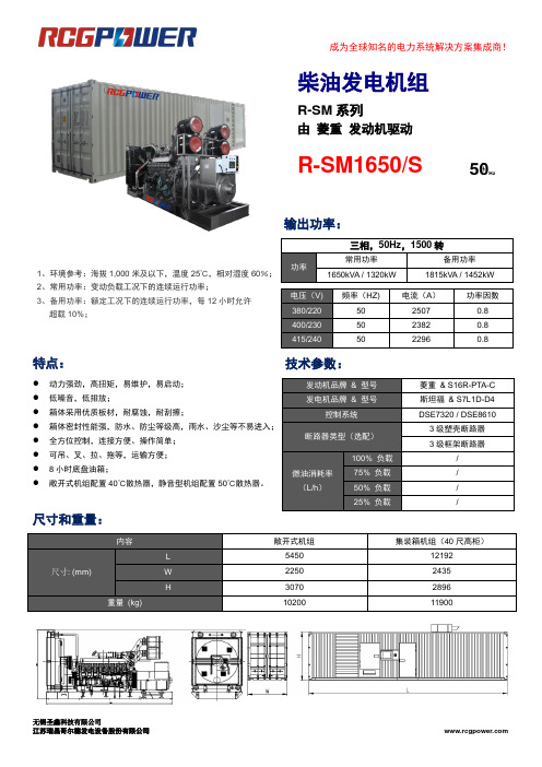
1、环境参考:海拔1,000米及以下,温度25℃,相对湿度60%;2、常用功率:变动负载工况下的连续运行功率;3、备用功率:额定工况下的连续运行功率,每12小时允许 超载10%;特点:⚫ 动力强劲,高扭矩,易维护,易启动; ⚫ 低噪音,低排放;⚫ 箱体采用优质板材,耐腐蚀,耐刮擦;⚫ 箱体密封性能强,防水、防尘等级高,雨水、沙尘等不易进入; ⚫ 全方位控制,连接方便、操作简单; ⚫ 可吊、叉、拉、拖等,运输方便; ⚫ 8小时底盘油箱;⚫ 敞开式机组配置40℃散热器,静音型机组配置50℃散热器。
尺寸和重量:内容敞开式机组 集装箱机组(40尺高柜)尺寸: (mm)L5450 12192 W 2250 2435 H3070 2896 重量 (kg)1020011900柴油发电机组R-SM 系列由 菱重 发动机驱动R-SM1650/S输出功率:三相,50Hz ,1500转功率 常用功率 备用功率 1650kVA / 1320kW1815kVA / 1452kW 技术参数:发动机品牌 & 型号 菱重 & S16R-PTA-C 发电机品牌 & 型号斯坦福 & S7L1D-D4 控制系统 DSE7320 / DSE8610 断路器类型(选配)3级塑壳断路器 3级框架断路器燃油消耗率(L/h )100% 负载/ 75% 负载 / 50% 负载 / 25% 负载/电压(V) 频率(HZ)电流(A ) 功率因数 380/220 50 2507 0.8 400/230 50 2382 0.8 415/2405022960.8发动机品牌 / 型号 & 菱重 / S16R-PTA-C缸数 / 排列 12 / V 功率(kW ) 常用 1450 类型 4冲程 备用1590 缸径 / 行程 170 mm / 180 mm压缩比 14 : 1 吸气方式 TCA 排量 (L) 65.37 冷却方式 水冷 调速方式 Electronic 润滑油15W40-CF4重量 (kg) 6750 润滑油容量(L )230冷却液容量(L )170发电机品牌 / 型号 & 斯坦福 / S7L1D-D4额定容量(kVA ) 1650 AVR 型号模拟式额定功率(kW ) 1320 电压调节(无负载、满载) ± 1.0% THF(BS EN60034 – 1) <2% 低速保护 标准 轴承数 单 防护等级IP23 绕组100% 铜 相序A(U), B(V), C(W)矽钢铁芯处理 整片冲孔TIF(NEMA MG 1-22) <50 绝缘等级 H 励磁系统 自励, 并联 绕组节距 2 / 3 环境温度 40℃ 阻尼绕组全部定子额定温度125 ℃控制系统 :DSE8610⚫ DSE8610是一种易于使用的机械轴连多发电机系统,设计为同步32的发电机,包括电子和非电子发动机。
Marlin固件全中文解析
3D打印机——Marlin固件全中文解析#ifndef CONFIGURATION_H#define CONFIGURATION_H// This configuration file contains the basic settings.// Advanced settings can be found in Configuration_adv.h// BASIC SETTINGS: select your board type, temperature sensor type, axis scaling, and endstop configuration//////////基本设置包括:主板类型,温度传感器类型,轴设置,限位开关配置//===================================================== ======================//============================= DELTA Printer===============================//===================================================== ======================// For a Delta printer replace the configuration files with the files in the// example_configurations/delta directory.////////////对于三角洲并联打印机,请找到固件里“example_configurations”文件夹下的“delta”子文件夹,并将其中的Configuration.h和Configuration_adv.h两个头文件拷贝到固件文件夹下,替换原先固件里的这两个头文件,并针对delta打印机作相应参数配置。
联想笔记本系列配置

3C产品培训sw

-USB 3.0 接口, 10倍于USB2.0的传输速度
多媒体娱乐体验
- 奥特蓝星扬声器,音质保证 - Sonic Focus音效软件,带来逼真的音效体验 - 支持UVD3第三代视屏解码引擎 分担CPU的占用率,高清播放更流畅
独特外观设计
- 3D效果上盖精致脱俗,彰显个性 - Wave键盘,带来舒适的打字手感 - 触摸板无缝设计,浑然一体,大方美观
2G DDR3 1333MHz, 4G DDR3 1333MHz (A84EI243SJ)
具有2组SOMIDMM内存扩展充槽 系统内存最高可扩充至 8GB(需操作系统支持) 320GB 5400rpm 500GB 5400rpm (A84EI243SJ) Windows7 Home Basic DOS (A84EI243SJ) 14.0” 16:9 LED背光屏幕 (1366*768) 内建多合一读卡器 支持MMC/SD/MS 内建DVD SuperMulti光驱 内建802.11 bgn无线网卡 内建10/100/1000Mbps以太网络模块
- 全球独家屏幕无亮点保证 - 华硕独家屏幕靓彩技术 - 预装Video Magic 影像画质提升软件
震撼听觉
完美视觉
优雅外观 精致细节
急速性能
- 荣获2010年 iF China设计大奖 - 铝合金拉丝屏幕上盖,优雅质感 - 全新波浪型流线侧边设计
- Intel Sandy bridge CPU i5-2410m
Celeron B815(1.6GHz) Intel GMA HD 2000 核心显卡 Intel HM65芯片组
显示屏 系统 读卡器 连接性 摄像头 接口 音效
14.0” 16:9 LED背光屏幕 (1366*768) DOS 内建多合一读卡器 支持MMC/SD/MS 内建802.11 bgn无线网卡 蓝牙™ V2.1 内建10/100/1000Mbps以太网络模块 30万像素高品质摄像头 2x USB 2.0 +1x USB 3.0 1 x VGA 接口 1 x HDMI 接口 1 x 以太网络接口 1x 麦克风输入插孔 1x 耳机输出插孔 Altec Lansing® Speakers(奥特蓝星扬声器)
HPcanon硒鼓适用机型对照大全

14
HP LaserJet 4000/4000N/4000T/4000TN/4050/4050T
/4050N/4050DN/4050TN/4000Se/4050USBMac/4050Se
C4127X(1010粉*2)有芯片
15
HP LaserJet 1000/1005/1200/1200n/1200 series/1220/1220 series
Q1338A(1010粉*4)有芯片
20
HP LaserJet 5200/5200L/5200LN /5200dtn/5200n/5200tn/5200Lx
Q7516A(1010粉*4或专用)有芯片
21
HP P2015d/2010/2014/2014n/M2727nfMFP/M2727nfsMFP
Q7553A(1010粉)有芯片
44
CANON LBP3018/3108/3010/3050
C912C(1008粉)
45
Canon LBP 3250
CB436A/313(1008粉)
46
CANON FAX-L95/100/100J/110/120/120J/140/140G/160/230/160G
CANON Image Class MF 4000/4100/4120/4122/4130/4150/4200/4600
5100LE/5000dn/5100DTN/5100TN
C4129X(1010粉*4或专用)有芯片
8
HP LaserJet 1100/1100A/1100A SE/1100A Xi/ 1100aAio/1100axiAio
/1100se/1100seAio/3200/3200m/3200se
广州大洋信息产品报价表(10-08-25)0

G450A系列
T4400“奔腾双核”64位笔记本电脑专用CPU(Duo2.1G/800FSB/1M/45nm)/ 14.0’WXGA LED背光屏 16:9黄金比例/2GB DDR3/320GHDD/超级DVD刻录/Geforce G210M独立显卡 512MB 独立显存 /10M-100M网卡内置 /DOS/802.11 B+G无线局域网卡/内置30万像素高清 T6600“奔腾双核”64位笔记本电脑专用CPU(Duo2.1G/800FSB/1M/45nm)/ 14.0’WXGA LED背光屏 16:9黄金比例/2GB DDR3/320GHDD/超级DVD刻录/Geforce G210M独立显卡 512MB 独立显存 /10M-100M网卡内置 /DOS/802.11 B+G无线局域网卡/内置30万像素高清
酷黑外观 Z465A系列
AMD® 速龙™ II 双核处理器P320 (2.1GHz,1MB二级缓存)/ 14.0’WXGA LED背光屏 16:9黄金比例/2GB DDR3/250GHDD/超级DVD刻录/ ATI HD 5470独立显卡 512M DDR3独立显存/10M-100M网卡/中文Windows 7 Home Basic /BGN无线局域网卡/内置30万像素高清摄像头/ HDMI高清输 出接口/联想一键拯救/联想软件礼包/酷黑外观 AMD® 羿龙™ II 三核处理器N830 (2.1GHz,1.5MB二级缓存)/ 14.0’ WXGA LED背光屏 16:9黄金比例/2GB DDR3/500GHDD/超级DVD刻录/ATI HD 5470独立显卡 512M DDR3独立显存/10M-100M网卡/中文Windows 7 Home Basic/BGN无线局域网卡/内置30万像素高清摄像头/ HDMI高清输 出接口/联想一键拯救/联想软件礼包/酷黑外观
H3N技术应用手册第4版

2.1 外形尺寸及安装尺寸 ......................................................................................... 4 2.2 安装环境 ........................................................................................................... 5 2.3 驱动器连接端子................................................................................................. 6 2.4 安装和配线时的注意事项 .................................................................................. 7
3.2.1 CN1 外形 ................................................................................................... 8 3.2.2 CN1 定义 ................................................................................................... 9 3.3 CN2 接口 .......................................................................................................... 9 3.3.1 CN2 外形 ................................................................................................... 9 3.3.2 CN2 定义 ................................................................................................. 10 3.4 输入输出接口类型 ........................................................................................... 11 3.4.1 数字信号输入接口.................................................................................... 11 3.4.2 数字信号输出接口.................................................................................... 11 3.4.3 脉冲指令输入接口.................................................................................... 12 3.4.4 模拟量输入接口 ....................................................................................... 13 3.4.5 编码器信号输出接口 ................................................................................ 13 3.4.6 编码器 Z 信号集电极开路输出接口.......................................................... 15 3.4.7 光电编码器信号输入接口......................................................................... 15 3.5 标准接线方式 .................................................................................................. 15 3.5.1 位置控制下标准接线图 ............................................................................ 15 3.5.2 速度/转矩模拟量控制下标准接线图 ......................................................... 17
NUC微控制器产品系列说明书

M251 Feature
。 Arm® Cortex®-M23 。 运行速度可达 48 MHz
M252 Feature
。 USB 2.0 全速设备无需外 挂晶振
M253 Feature
。 USB 2.0 全速设备无需外 挂晶振
。 高达五路 UART 。 CAN FD x1
2
Low Power
TrustZone
AEC-Q100
Market Trend
随着电子应用对低功耗或电池供电的需 求日益增加,现今的应用必须尽量降低 能源消耗,甚至在极端情况下,可能需 要倚赖单颗电池来维持长达 15 至 20 年 运转
低功耗应用情景包含手持式设备、居家、 AIoT、IIoT (工业物联网) 等应用情景, 使用范围十分广泛
(Programmable Serial I/O) • USB 2.0 全速装置无需外挂晶振 • 独立的 RTC 电源 VBAT 管脚
Highlight
• 支持 1.8 V ~ 5.5 V 串行接口,可连接不同电压 装置
*USCI: Universal Serial Control Interface Controller
C
1.8 3.3 5 M253
CU
3.3 5 M071
1.8 3.3 5 M252
U
3.3 5 M051
1.8 3.3 5 M251
3.3 5 Mini51
3.3 5 3.3 5
1.8 3.3 Nano100
M480 M460 M471 M453 M452 M451
E CU E CU
U C
U
Arm9™
- 1、下载文档前请自行甄别文档内容的完整性,平台不提供额外的编辑、内容补充、找答案等附加服务。
- 2、"仅部分预览"的文档,不可在线预览部分如存在完整性等问题,可反馈申请退款(可完整预览的文档不适用该条件!)。
- 3、如文档侵犯您的权益,请联系客服反馈,我们会尽快为您处理(人工客服工作时间:9:00-18:30)。
1/40October 2004M95160M9508016Kbit and 8Kbit Serial SPI Bus EEPROMWith High Speed ClockFEATURES SUMMARY■Compatible with SPI Bus Serial Interface (Positive Clock SPI Modes)■Single Supply Voltage:– 4.5 to 5.5V for M95xxx – 2.5 to 5.5V for M95xxx-W – 1.8 to 5.5V for M95xxx-R ■High Speed–10MHz Clock Rate, 5ms Write Time ■Status Register■Hardware Protection of the Status Register ■BYTE and PAGE WRITE (up to 32 Bytes)■Self-Timed Programming Cycle■Adjustable Size Read-Only EEPROM Area ■Enhanced ESD Protection■More than 1 Million Erase/Write Cycles ■More than 40-Year Data RetentionTable 1. Product ListReferencePart NumberM95160M95160M95160-W M95160-R M95080M95080M95080-W M95080-RM95160, M95080TABLE OF CONTENTSFEATURES SUMMARY . . . . . . . . . . . . . . . . . . . . . . . . . . . . . . . . . . . . . . . . . . . . . . . . . . . . . . . . . . . . .1Table 1.Product List . . . . . . . . . . . . . . . . . . . . . . . . . . . . . . . . . . . . . . . . . . . . . . . . . . . . . . . . . . . .1 Figure 1.Packages. . . . . . . . . . . . . . . . . . . . . . . . . . . . . . . . . . . . . . . . . . . . . . . . . . . . . . . . . . . . . .1SUMMARY DESCRIPTION. . . . . . . . . . . . . . . . . . . . . . . . . . . . . . . . . . . . . . . . . . . . . . . . . . . . . . . . . . .5Figure 2.Logic Diagram . . . . . . . . . . . . . . . . . . . . . . . . . . . . . . . . . . . . . . . . . . . . . . . . . . . . . . . . . .5 Figure 3.DIP, SO, TSSOP and MLP Connections (Top View). . . . . . . . . . . . . . . . . . . . . . . . . . . . .5 Table 2.Signal Names . . . . . . . . . . . . . . . . . . . . . . . . . . . . . . . . . . . . . . . . . . . . . . . . . . . . . . . . . .5SIGNAL DESCRIPTION . . . . . . . . . . . . . . . . . . . . . . . . . . . . . . . . . . . . . . . . . . . . . . . . . . . . . . . . . . . . .6 Serial Data Output (Q). . . . . . . . . . . . . . . . . . . . . . . . . . . . . . . . . . . . . . . . . . . . . . . . . . . . . . . . . . . .6 Serial Data Input (D) . . . . . . . . . . . . . . . . . . . . . . . . . . . . . . . . . . . . . . . . . . . . . . . . . . . . . . . . . . . . .6 Serial Clock (C). . . . . . . . . . . . . . . . . . . . . . . . . . . . . . . . . . . . . . . . . . . . . . . . . . . . . . . . . . . . . . . . .6 Chip Select (S) . . . . . . . . . . . . . . . . . . . . . . . . . . . . . . . . . . . . . . . . . . . . . . . . . . . . . . . . . . . . . . . . .6 Hold (HOLD) . . . . . . . . . . . . . . . . . . . . . . . . . . . . . . . . . . . . . . . . . . . . . . . . . . . . . . . . . . . . . . . . . . .6 Write Protect (W). . . . . . . . . . . . . . . . . . . . . . . . . . . . . . . . . . . . . . . . . . . . . . . . . . . . . . . . . . . . . . . .6CONNECTING TO THE SPI BUS. . . . . . . . . . . . . . . . . . . . . . . . . . . . . . . . . . . . . . . . . . . . . . . . . . . . . .7Figure 4.Bus Master and Memory Devices on the SPI Bus. . . . . . . . . . . . . . . . . . . . . . . . . . . . . . .7 SPI Modes . . . . . . . . . . . . . . . . . . . . . . . . . . . . . . . . . . . . . . . . . . . . . . . . . . . . . . . . . . . . . . . . . . . .8 Figure 5.SPI Modes Supported . . . . . . . . . . . . . . . . . . . . . . . . . . . . . . . . . . . . . . . . . . . . . . . . . . . .8OPERATING FEATURES. . . . . . . . . . . . . . . . . . . . . . . . . . . . . . . . . . . . . . . . . . . . . . . . . . . . . . . . . . . .9Power-up . . . . . . . . . . . . . . . . . . . . . . . . . . . . . . . . . . . . . . . . . . . . . . . . . . . . . . . . . . . . . . . . . . . . .9 Power On Reset: VCC Lock-Out Write Protect. . . . . . . . . . . . . . . . . . . . . . . . . . . . . . . . . . . . . . .9 Power-down. . . . . . . . . . . . . . . . . . . . . . . . . . . . . . . . . . . . . . . . . . . . . . . . . . . . . . . . . . . . . . . . . . .9 Active Power and Standby Power Modes. . . . . . . . . . . . . . . . . . . . . . . . . . . . . . . . . . . . . . . . . . .9 Hold Condition. . . . . . . . . . . . . . . . . . . . . . . . . . . . . . . . . . . . . . . . . . . . . . . . . . . . . . . . . . . . . . . . .9 Status Register . . . . . . . . . . . . . . . . . . . . . . . . . . . . . . . . . . . . . . . . . . . . . . . . . . . . . . . . . . . . . . .10 WIP bit. . . . . . . . . . . . . . . . . . . . . . . . . . . . . . . . . . . . . . . . . . . . . . . . . . . . . . . . . . . . . . . . . . . . . . .10 WEL bit . . . . . . . . . . . . . . . . . . . . . . . . . . . . . . . . . . . . . . . . . . . . . . . . . . . . . . . . . . . . . . . . . . . . . .10 BP1, BP0 bits . . . . . . . . . . . . . . . . . . . . . . . . . . . . . . . . . . . . . . . . . . . . . . . . . . . . . . . . . . . . . . . . .10 SRWD bit. . . . . . . . . . . . . . . . . . . . . . . . . . . . . . . . . . . . . . . . . . . . . . . . . . . . . . . . . . . . . . . . . . . . .10 Table 3.Status Register Format . . . . . . . . . . . . . . . . . . . . . . . . . . . . . . . . . . . . . . . . . . . . . . . . . .10 Data Protection and Protocol Control. . . . . . . . . . . . . . . . . . . . . . . . . . . . . . . . . . . . . . . . . . . . .10 Table 4.Write-Protected Block Size . . . . . . . . . . . . . . . . . . . . . . . . . . . . . . . . . . . . . . . . . . . . . . .10MEMORY ORGANIZATION . . . . . . . . . . . . . . . . . . . . . . . . . . . . . . . . . . . . . . . . . . . . . . . . . . . . . . . . .11 Figure 6.Block Diagram. . . . . . . . . . . . . . . . . . . . . . . . . . . . . . . . . . . . . . . . . . . . . . . . . . . . . . . . .11INSTRUCTIONS . . . . . . . . . . . . . . . . . . . . . . . . . . . . . . . . . . . . . . . . . . . . . . . . . . . . . . . . . . . . . . . . . .12 Table 5.Instruction Set . . . . . . . . . . . . . . . . . . . . . . . . . . . . . . . . . . . . . . . . . . . . . . . . . . . . . . . . .12 Write Enable (WREN) . . . . . . . . . . . . . . . . . . . . . . . . . . . . . . . . . . . . . . . . . . . . . . . . . . . . . . . . . .132/40M95160, M95080Figure 7.Write Enable (WREN) Sequence. . . . . . . . . . . . . . . . . . . . . . . . . . . . . . . . . . . . . . . . . . .13 Write Disable (WRDI). . . . . . . . . . . . . . . . . . . . . . . . . . . . . . . . . . . . . . . . . . . . . . . . . . . . . . . . . . .13 Figure 8.Write Disable (WRDI) Sequence. . . . . . . . . . . . . . . . . . . . . . . . . . . . . . . . . . . . . . . . . . .13 Read Status Register (RDSR). . . . . . . . . . . . . . . . . . . . . . . . . . . . . . . . . . . . . . . . . . . . . . . . . . . .14 WIP bit. . . . . . . . . . . . . . . . . . . . . . . . . . . . . . . . . . . . . . . . . . . . . . . . . . . . . . . . . . . . . . . . . . . . . . .14 WEL bit . . . . . . . . . . . . . . . . . . . . . . . . . . . . . . . . . . . . . . . . . . . . . . . . . . . . . . . . . . . . . . . . . . . . . .14 BP1, BP0 bits . . . . . . . . . . . . . . . . . . . . . . . . . . . . . . . . . . . . . . . . . . . . . . . . . . . . . . . . . . . . . . . . .14 SRWD bit. . . . . . . . . . . . . . . . . . . . . . . . . . . . . . . . . . . . . . . . . . . . . . . . . . . . . . . . . . . . . . . . . . . . .14 Figure 9.Read Status Register (RDSR) Sequence . . . . . . . . . . . . . . . . . . . . . . . . . . . . . . . . . . . .14 Write Status Register (WRSR) . . . . . . . . . . . . . . . . . . . . . . . . . . . . . . . . . . . . . . . . . . . . . . . . . . .15 Table 6.Protection Modes. . . . . . . . . . . . . . . . . . . . . . . . . . . . . . . . . . . . . . . . . . . . . . . . . . . . . . .15 Table 7.Address Range Bits. . . . . . . . . . . . . . . . . . . . . . . . . . . . . . . . . . . . . . . . . . . . . . . . . . . . .16 Figure 10.Write Status Register (WRSR) Sequence. . . . . . . . . . . . . . . . . . . . . . . . . . . . . . . . . . . .16 Read from Memory Array (READ) . . . . . . . . . . . . . . . . . . . . . . . . . . . . . . . . . . . . . . . . . . . . . . . .17 Figure 11.Read from Memory Array (READ) Sequence. . . . . . . . . . . . . . . . . . . . . . . . . . . . . . . . .17 Write to Memory Array (WRITE). . . . . . . . . . . . . . . . . . . . . . . . . . . . . . . . . . . . . . . . . . . . . . . . . .18 Figure 12.Byte Write (WRITE) Sequence . . . . . . . . . . . . . . . . . . . . . . . . . . . . . . . . . . . . . . . . . . . .18 Figure 13.Page Write (WRITE) Sequence . . . . . . . . . . . . . . . . . . . . . . . . . . . . . . . . . . . . . . . . . . .19POWER-UP AND DELIVERY STATE. . . . . . . . . . . . . . . . . . . . . . . . . . . . . . . . . . . . . . . . . . . . . . . . . .20Power-up State . . . . . . . . . . . . . . . . . . . . . . . . . . . . . . . . . . . . . . . . . . . . . . . . . . . . . . . . . . . . . . .20 Initial Delivery State . . . . . . . . . . . . . . . . . . . . . . . . . . . . . . . . . . . . . . . . . . . . . . . . . . . . . . . . . . .20MAXIMUM RATING. . . . . . . . . . . . . . . . . . . . . . . . . . . . . . . . . . . . . . . . . . . . . . . . . . . . . . . . . . . . . . . .21 Table 8.Absolute Maximum Ratings. . . . . . . . . . . . . . . . . . . . . . . . . . . . . . . . . . . . . . . . . . . . . . .21DC AND AC PARAMETERS. . . . . . . . . . . . . . . . . . . . . . . . . . . . . . . . . . . . . . . . . . . . . . . . . . . . . . . . .22Table 9.Operating Conditions (M95xxx). . . . . . . . . . . . . . . . . . . . . . . . . . . . . . . . . . . . . . . . . . . .22 Table 10.Operating Conditions (M95xxx-W). . . . . . . . . . . . . . . . . . . . . . . . . . . . . . . . . . . . . . . . . .22 Table 11.Operating Conditions (M95xxx-R). . . . . . . . . . . . . . . . . . . . . . . . . . . . . . . . . . . . . . . . . .22 Table 12.AC Measurement Conditions. . . . . . . . . . . . . . . . . . . . . . . . . . . . . . . . . . . . . . . . . . . . . .22 Figure 14.AC Measurement I/O Waveform. . . . . . . . . . . . . . . . . . . . . . . . . . . . . . . . . . . . . . . . . . .22 Table 13.Capacitance. . . . . . . . . . . . . . . . . . . . . . . . . . . . . . . . . . . . . . . . . . . . . . . . . . . . . . . . . . .23 Table 14.DC Characteristics (M95xxx, Device Grade 6) . . . . . . . . . . . . . . . . . . . . . . . . . . . . . . . .23 Table 15.DC Characteristics (M95xxx, Device Grade 3) . . . . . . . . . . . . . . . . . . . . . . . . . . . . . . . .24 Table 16.DC Characteristics (M95xxx-W, Device Grade 6). . . . . . . . . . . . . . . . . . . . . . . . . . . . . .24 Table 17.DC Characteristics (M95xxx-W, Device Grade 3). . . . . . . . . . . . . . . . . . . . . . . . . . . . . .25 Table 18.DC Characteristics (M95xxx-R). . . . . . . . . . . . . . . . . . . . . . . . . . . . . . . . . . . . . . . . . . . .25 Table 19.AC Characteristics (M95xxx, Device Grade 6) . . . . . . . . . . . . . . . . . . . . . . . . . . . . . . . .26 Table 20.AC Characteristics (M95xxx, Device Grade 3) . . . . . . . . . . . . . . . . . . . . . . . . . . . . . . . .27 Table 21.AC Characteristics (M95xxx-W, Device Grade 6) . . . . . . . . . . . . . . . . . . . . . . . . . . . . . .28 Table 22.AC Characteristics (M95xxx-W, Device Grade 3) . . . . . . . . . . . . . . . . . . . . . . . . . . . . . .29 Table 23.AC Characteristics (M95xxx-R). . . . . . . . . . . . . . . . . . . . . . . . . . . . . . . . . . . . . . . . . . . .30 Figure 15.Serial Input Timing . . . . . . . . . . . . . . . . . . . . . . . . . . . . . . . . . . . . . . . . . . . . . . . . . . . . .31 Figure 16.Hold Timing. . . . . . . . . . . . . . . . . . . . . . . . . . . . . . . . . . . . . . . . . . . . . . . . . . . . . . . . . . .31 Figure 17.Output Timing . . . . . . . . . . . . . . . . . . . . . . . . . . . . . . . . . . . . . . . . . . . . . . . . . . . . . . . . .323/40M95160, M95080PACKAGE MECHANICAL . . . . . . . . . . . . . . . . . . . . . . . . . . . . . . . . . . . . . . . . . . . . . . . . . . . . . . . . . .33Figure 18.PDIP8 – 8 pin Plastic DIP, 0.25mm lead frame, Package Outline . . . . . . . . . . . . . . . . .33 Table 24.PDIP8 – 8 pin Plastic DIP, 0.25mm lead frame, Package Mechanical Data. . . . . . . . . .33 Figure 19.SO8 narrow – 8 lead Plastic Small Outline, 150 mils body width, Package Outline . . . .34 Table 25.SO8 narrow – 8 lead Plastic Small Outline, 150 mils body width, Mechanical Data. . . .34 Figure 20.UFDFPN8 (MLP8) 8-lead Ultra thin Fine pitch Dual Flat Package No lead 2x3mm², Outline 35Table 26.UFDFPN8 (MLP8) 8-lead Ultra thin Fine pitch Dual Flat Package No lead 2x3mm², Data.35Figure 21.TSSOP8 – 8 lead Thin Shrink Small Outline, Package Outline . . . . . . . . . . . . . . . . . . .36 Table 27.TSSOP8 – 8 lead Thin Shrink Small Outline, Package Mechanical Data. . . . . . . . . . . .36 Figure 22.TSSOP8 3x3mm² – 8 lead Thin Shrink Small Outline, 3x3mm² body size, Package Outline 37Table 28.TSSOP8 3x3mm² – 8 lead Thin Shrink Small Outline, 3x3mm² body size, Mechanical Data 37PART NUMBERING . . . . . . . . . . . . . . . . . . . . . . . . . . . . . . . . . . . . . . . . . . . . . . . . . . . . . . . . . . . . . . .38Table 29.Ordering Information Scheme . . . . . . . . . . . . . . . . . . . . . . . . . . . . . . . . . . . . . . . . . . . . .38 Table 30.How to Identify Present and Previous Products by the Process Identification Letter . . .38REVISION HISTORY. . . . . . . . . . . . . . . . . . . . . . . . . . . . . . . . . . . . . . . . . . . . . . . . . . . . . . . . . . . . . . .39 Table 31.Document Revision History. . . . . . . . . . . . . . . . . . . . . . . . . . . . . . . . . . . . . . . . . . . . . . .394/40M95160, M95080 SUMMARY DESCRIPTIONThese electrically erasable programmable memo-ry (EEPROM) devices are accessed by a high speed SPI-compatible bus. The memory array is organized as 2048 x 8 bit (M95160), and 1024 x 8 bit (M95080).The device is accessed by a simple serial interface that is SPI-compatible. The bus signals are C, D and Q, as shown in Table 2. and Figure 2..The device is selected when Chip Select (S) is tak-en Low. Communications with the device can be interrupted using Hold (HOLD).Figure 3. DIP, SO, TSSOP and MLPsions, and how to identify pin-1.Table 2. Signal NamesC SerialClockD Serial Data InputQ Serial Data OutputS Chip SelectW WriteProtectHOLD HoldV CC Supply VoltageV SS Ground5/40M95160, M950806/40SIGNAL DESCRIPTIONDuring all operations, V CC must be held stable and within the specified valid range: V CC (min) to V CC (max).All of the input and output signals must be held High or Low (according to voltages of V IH , V OH , V IL or V OL , as specified in Table 14. to Table 18.).These signals are described next.Serial Data Output (Q).This output signal is used to transfer data serially out of the device.Data is shifted out on the falling edge of Serial Clock (C).Serial Data Input (D).This input signal is used to transfer data serially into the device. It receives in-structions, addresses, and the data to be written.Values are latched on the rising edge of Serial Clock (C).Serial Clock (C).This input signal provides the timing of the serial interface. Instructions, address-es, or data present at Serial Data Input (D) are latched on the rising edge of Serial Clock (C). Data on Serial Data Output (Q) changes after the falling edge of Serial Clock (C).Chip Select (S).When this input signal is High,the device is deselected and Serial Data Output(Q) is at high impedance. Unless an internal Write cycle is in progress, the device will be in the Stand-by Power mode. Driving Chip Select (S) Low se-lects the device, placing it in the Active Power mode.After Power-up, a falling edge on Chip Select (S)is required prior to the start of any instruction. pause any serial communications with the device without deselecting the device.During the Hold condition, the Serial Data Output (Q) is high impedance, and Serial Data Input (D)and Serial Clock (C) are Don’t Care.To start the Hold condition, the device must be se-The main purpose of this in-put signal is to freeze the size of the area of mem-ory that is protected against Write instructions (as specified by the values in the BP1 and BP0 bits of the Status Register).This pin must be driven either High or Low, and must be stable during all write instructions.M95160, M95080 CONNECTING TO THE SPI BUSThese devices are fully compatible with the SPI protocol.All instructions, addresses and input data bytes are shifted in to the device, most significant bit first. The Serial Data Input (D) is sampled on the first rising edge of the Serial Clock (C) after Chip Select (S) goes Low.All output data bytes are shifted out of the device, most significant bit first. The Serial Data Output (Q) is latched on the first falling edge of the Serial Clock (C) after the instruction (such as the Read from Memory Array and Read Status Register in-structions) have been clocked into the device. Figure 4. shows three devices, connected to an MCU, on a SPI bus. Only one device is selected at a time, so only one device drives the Serial Data Output (Q) line at a time, all the others being high impedance.7/40M95160, M950808/40SPI ModesThese devices can be driven by a microcontroller with its SPI peripheral running in either of the two following modes:–CPOL=0, CPHA=0–CPOL=1, CPHA=1For these two modes, input data is latched in on the rising edge of Serial Clock (C), and output data is available from the falling edge of Serial Clock (C).The difference between the two modes, as shown in Figure 5., is the clock polarity when the bus master is in Stand-by mode and not transferring data:– C remains at 0 for (CPOL=0, CPHA=0)– C remains at 1 for (CPOL=1, CPHA=1)M95160, M95080 OPERATING FEATURESPower-upWhen the power supply is turned on, V CC rises from V SS to V CC.During this time, the Chip Select (S) must be al-lowed to follow the V CC voltage. It must not be al-lowed to float, but should be connected to V CC via a suitable pull-up resistor.sensitive as well as level sensitive. After Power-up, the device does not become selected until a falling edge has first been detected on Chip Select been High, prior to going Low to start the first op-eration.Power On Reset: V CC Lock-Out Write Protect In order to prevent data corruption and inadvertent Write instructions during Power-up, a Power On Reset (POR) circuit is included. The internal reset is held active until V CC has reached the Power On Reset (POR) threshold voltage, and all operations are disabled – the device will not respond to any instruction. In the same way, when V CC drops from the operating voltage, below the Power On Reset (POR) threshold voltage, all operations are dis-abled and the device will not respond to any in-struction.A stable and valid V CC must be applied before ap-plying any logic signal.Power-downAt Power-down, the device must be deselected. voltage applied on V CC.Active Power and Standby Power Modesed, and in the Active Power mode. The device consumes I CC, as specified in Table 14. to Table 18..lected. If an Erase/Write cycle is not currently in progress, the device then goes in to the Standby Power mode, and the device consumption drops to I CC1.Hold Conditionrial communications with the device without reset-ting the clocking sequence.During the Hold condition, the Serial Data Output (Q) is high impedance, and Serial Data Input (D) and Serial Clock (C) are Don’t Care.To enter the Hold condition, the device must be selected, with Chip Select (S) Low.Normally, the device is kept selected, for the whole duration of the Hold condition. Deselecting the de-vice while it is in the Hold condition, has the effect of resetting the state of the device, and this mech-anism can be used if it is required to reset any pro-cesses that had been in progress.signal is driven Low at the same time as Serial Clock (C) already being Low.The Hold condition ends when the Hold (HOLD) signal is driven High at the same time as Serial Clock (C) already being Low.9/40M95160, M9508010/40Status RegisterFigure 6. shows the position of the Status Register in the control logic of the device. The Status Reg-ister contains a number of status and control bits that can be read or set (as appropriate) by specific instructions.WIP bit.The Write In Progress (WIP) bit indicates whether the memory is busy with a Write or Write Status Register cycle.WEL bit.The Write Enable Latch (WEL) bit indi-cates the status of the internal Write Enable Latch.BP1, BP0 bits.The Block Protect (BP1, BP0) bits are non-volatile. They define the size of the area to be software protected against Write instructions. SRWD bit.The Status Register Write Disable (SRWD) bit is operated in conjunction with the Write Protect (W) signal. The Status Register signal allow the device to be put in the Hardware Protected mode. In this mode, the non-volatile bits of the Status Register (SRWD, BP1, BP0) become read-only bits.Table 3. Status Register FormatData Protection and Protocol ControlNon-volatile memory devices can be used in envi-ronments that are particularly noisy, and within ap-plications that could experience problems if memory bytes are corrupted. Consequently, the device features the following data protection mechanisms:■Write and Write Status Register instructionsare checked that they consist of a number of clock pulses that is a multiple of eight, before they are accepted for execution.■All instructions that modify data must bepreceded by a Write Enable (WREN) instruction to set the Write Enable Latch(WEL) bit. This bit is returned to its reset state by the following events:–Power-up–Write Disable (WRDI) instructioncompletion–Write Status Register (WRSR) instructioncompletion–Write (WRITE) instruction completion ■The Block Protect (BP1, BP0) bits allow part ofthe memory to be configured as read-only. This is the Software Protected Mode (SPM).■The Write Protect (W) signal allows the BlockProtect (BP1, BP0) bits to be protected. This is the Hardware Protected Mode (HPM).For any instruction to be accepted, and executed,Chip Select (S) must be driven High after the rising edge of Serial Clock (C) for the last bit of the in-struction, and before the next rising edge of Serial Clock (C).Two points need to be noted in the previous sen-tence:–The ‘last bit of the instruction’ can be theeighth bit of the instruction code, or the eighth bit of a data byte, depending on the instruction (except for Read Status Register (RDSR) and Read (READ) instructions).–The ‘next rising edge of Serial Clock (C)’ might(or might not) be the next bus transaction for some other device on the SPI bus.Table 4. Write-Protected Block Sizeb7 b0SRWD0 0 0 BP1 BP0 WEL WIPStatus Register Write ProtectBlock Protect Bits Write Enable Latch BitWrite In Progress BitStatus Register BitsProtected BlockArray Addresses Protected BP1 BP0 M95160 M950800 0 nonenone none 0 1 Upper quarter 0600h - 07FFh 0300h - 03FFh 1 0 Upper half 0400h - 07FFh 0200h - 03FFh 11Whole memory0000h - 07FFh0000h - 03FFhMEMORY ORGANIZATIONThe memory is organized as shown in Figure 6..11/40INSTRUCTIONSEach instruction starts with a single-byte code, as summarized in Table 5..If an invalid instruction is sent (one not contained in Table 5.), the device automatically deselects it-self.Table 5. Instruction SetInstructionDescriptionInstructionFormat WREN Write Enable0000 0110 WRDI Write Disable0000 0100 RDSR Read Status Register 0000 0101 WRSR Write Status Register 0000 0001 READ Read from Memory Array0000 0011 WRITE Write to Memory Array 0000 001012/40Write Enable (WREN)The Write Enable Latch (WEL) bit must be set pri-or to each WRITE and WRSR instruction. The only way to do this is to send a Write Enable instruction to the device.As shown in Figure 7., to send this instruction to the device, Chip Select (S) is driven Low, and the bits of the instruction byte are shifted in, on Serial Data Input (D). The device then enters a wait state. It waits for a the device to be deselected, by Chip Select (S) being driven High.One way of resetting the Write Enable Latch (WEL) bit is to send a Write Disable instruction to the device.As shown in Figure 8., to send this instruction to the device, Chip Select (S) is driven Low, and the bits of the instruction byte are shifted in, on Serial Data Input (D).The device then enters a wait state. It waits for a the device to be deselected, by Chip Select (S) be-ing driven High.The Write Enable Latch (WEL) bit, in fact, be-comes reset by any of the following events:–Power-up–WRDI instruction execution–WRSR instruction completion–WRITE instruction completion.13/40Read Status Register (RDSR)The Read Status Register (RDSR) instruction al-lows the Status Register to be read. The Status Register may be read at any time, even while a Write or Write Status Register cycle is in progress. When one of these cycles is in progress, it is rec-ommended to check the Write In Progress (WIP) bit before sending a new instruction to the device. It is also possible to read the Status Register con-tinuously, as shown in Figure 9..The status and control bits of the Status Register are as follows:WIP bit.The Write In Progress (WIP) bit indicates whether the memory is busy with a Write or Write Status Register cycle. When set to 1, such a cycle is in progress, when reset to 0 no such cycle is in progress.WEL bit.The Write Enable Latch (WEL) bit indi-cates the status of the internal Write Enable Latch. When set to 1 the internal Write Enable Latch is set, when set to 0 the internal Write Enable Latch is reset and no Write or Write Status Register in-struction is accepted.BP1, BP0 bits.The Block Protect (BP1, BP0) bits are non-volatile. They define the size of the area to be software protected against Write instructions. These bits are written with the Write Status Regis-ter (WRSR) instruction. When one or both of the Block Protect (BP1, BP0) bits is set to 1, the rele-vant memory area (as defined in Table 3.) be-comes protected against Write (WRITE) instructions. The Block Protect (BP1, BP0) bits can be written provided that the Hardware Protect-ed mode has not been set.SRWD bit.The Status Register Write Disable (SRWD) bit is operated in conjunction with the Write Protect (W) signal. The Status Register Write Disable (SRWD) bit and Write Protect (W) signal allow the device to be put in the Hardware Protected mode (when the Status Register Write Disable (SRWD) bit is set to 1, and Write Protect bits of the Status Register (SRWD, BP1, BP0) be-come read-only bits and the Write Status Register (WRSR) instruction is no longer accepted for exe-cution.14/40Write Status Register (WRSR)The Write Status Register (WRSR) instruction al-lows new values to be written to the Status Regis-ter. Before it can be accepted, a Write Enable (WREN) instruction must previously have been ex-ecuted. After the Write Enable (WREN) instruction has been decoded and executed, the device sets the Write Enable Latch (WEL).The Write Status Register (WRSR) instruction is entered by driving Chip Select (S) Low, followed by the instruction code and the data byte on Serial Data Input (D).The instruction sequence is shown in Figure 10.. The Write Status Register (WRSR) instruction has no effect on b6, b5, b4, b1 and b0 of the Status Register. b6, b5 and b4 are always read as 0. Chip Select (S) must be driven High after the rising edge of Serial Clock (C) that latches in the eighth bit of the data byte, and before the next rising edge of Serial Clock (C). Otherwise, the Write Status Register (WRSR) instruction is not executed. As soon as Chip Select (S) is driven High, the self-timed Write Status Register cycle (whose duration is t W) is initiated. While the Write Status Register cycle is in progress, the Status Register may still be read to check the value of the Write In Progress (WIP) bit. The Write In Progress (WIP) bit is 1 dur-ing the self-timed Write Status Register cycle, and is 0 when it is completed. When the cycle is com-pleted, the Write Enable Latch (WEL) is reset. The Write Status Register (WRSR) instruction al-lows the user to change the values of the Block Protect (BP1, BP0) bits, to define the size of the area that is to be treated as read-only, as defined in Table 3..The Write Status Register (WRSR) instruction also allows the user to set or reset the Status Register Write Disable (SRWD) bit in accordance with the Write Protect (W) signal. The Status Register Write Disable (SRWD) bit and Write Protect (W) signal allow the device to be put in the Hardware Protected Mode (HPM). The Write Status Register (WRSR) instruction is not executed once the Hard-ware Protected Mode (HPM) is entered.The contents of the Status Register Write Disable (SRWD) and Block Protect (BP1, BP0) bits are fro-zen at their current values from just before the start of the execution of Write Status Register (WRSR) instruction. The new, updated, values take effect at the moment of completion of the ex-ecution of Write Status Register (WRSR) instruc-tion.Table 6. Protection ModesNote: 1.As defined by the values in the Block Protect (BP1, BP0) bits of the Status Register, as shown in Table 6..The protection features of the device are summa-rized in Table 4..When the Status Register Write Disable (SRWD) bit of the Status Register is 0 (its initial delivery state), it is possible to write to the Status Register provided that the Write Enable Latch (WEL) bit has previously been set by a Write Enable (WREN) in-struction, regardless of the whether Write Protect (W) is driven High or Low.When the Status Register Write Disable (SRWD) bit of the Status Register is set to 1, two cases need to be considered, depending on the state of –If Write Protect (W) is driven High, it is possible to write to the Status Registerprovided that the Write Enable Latch (WEL) bit has previously been set by a Write Enable(WREN) instruction.–If Write Protect (W) is driven Low, it is not possible to write to the Status Register even if the Write Enable Latch (WEL) bit haspreviously been set by a Write Enable(WREN) instruction. (Attempts to write to the Status Register are rejected, and are notaccepted for execution). As a consequence,all the data bytes in the memory area that are software protected (SPM) by the Block ProtectW Signal SRWDBitModeWrite Protection of theStatus RegisterMemory ContentProtected Area1Unprotected Area110SoftwareProtected(SPM)Status Register is Writable(if the WREN instructionhas set the WEL bit)The values in the BP1 andBP0 bits can be changedWrite ProtectedReady to accept Writeinstructions00 1101HardwareProtected(HPM)Status Register isHardware write protectedThe values in the BP1 andBP0 bits cannot bechangedWrite ProtectedReady to accept Writeinstructions15/40。