BT137-800E中文资料
BT137 数据手册说明书

主要参数 MAIN CHARACTERISTICSI T(RMS) 8A V DRM 600V or 800VI GT 10mA用途APPLICATIONSz 交流开关 z AC switching z 相位控制 z Phase control产品特性FEATURESz 平面钝化芯片高可靠性、一致性 z Planar chip for reliabilityand uniformz 低通态电流和高浪涌电流能力 z High I TSM z 环保RoHS 产品z RoHS productsz 通过UL 认证: E258645z UL :E258645订货信息 ORDER MESSAGES订 货 型 号 Order code印 记 Marking封 装 Package包 装 PackagingBT137-O-Z-N-C BT137 TO-220 袋装 Bag BT137-O-J-N-B BT137 TO-220S 条管 Tube BT137-O-HF-N-B BT137TO-220HF 条管 Tube绝对最大额定值 ABSOLUTE RATINGS (T C =25℃)项 目 Parameter符 号Symbol 试 验 条 件 Condition数 值Value 单位Unit重复峰值断态电压Repetitive peak off-state voltage V DRM±600 ±800 V 通态方均根电流On-state RMS current I T(RMS)full sine wave 8 A full sine wave ,t=20ms 65 A 非重复浪涌峰值通态电流Non- repetitive surge peak on-state current I TSMfull sine wave ,t=16.7ms 71AI 2t t =10ms 21 A 2s 通态电流临界上升率Repetitive rate ofrise of on-state current after triggering dI/dtI TM =12A, I G =0.2A, dI G /dt=0.2A/μs50 A/μs 峰值门极电流 Peak gate current I GM 2 A 峰值门极电压 Peak gate voltage V GM 5 V 峰值门极功率 Peak gate power P GM 5 W 平均门极功率 Average gate power P G(AV)over any 20ms period0.5W存储温度 Storage temperatureT stg -40~150 ℃ 操作结温Operation junction temperatureT VJ125 ℃电特性 ELECTRICAL CHARACTERISTIC (T C =25℃)项 目 Parameter符 号 Symbol测 试 条 件 Condition最小Min典型 Typ 最大 Max 单位Unit峰值重复断态电流Peak Repetitive Blocking CurrentI DRMV DM =V DRM , Tj=125℃,gate open- 0.10.5 mA峰值通态电压Peak on-state voltageV TM I TM =10A - 1.3 1.65 VMT1(-),MT2(+),G(+)- 2.5 10 mA MT1(-),MT2(+),G(-)- 4.0 10 mA MT1(+),MT2(-),G(-)- 5.0 10 mA 门极触发电流Gate trigger currentI GTV DM =12V,R L =100ΩMT1(+),MT2(-),G(+)- 11 25 mA MT1(-),MT2(+),G(+)- - 1.5 V MT1(-),MT2(+),G(-)- - 1.5 V 门极触发电压Gate trigger voltage V GTV DM =12V,R L =100ΩMT1(+),MT2(-),G(-)- - 1.5 V维持电流Holding current I H V DM =12V, I GT =0.1A - - 20 mAMT1(-),MT2(+),G(+)- 3.0 25 mA MT1(-),MT2(+),G(-)- 14 35 mA 擎住电流Latching current I LV DM =12V,I GT =0.1AMT1(+),MT2(-),G(-)- 3.0 25 mA 断态临界电压上升率 Rise of off- state voltagedV/dtV DM =67% V DRM(MAX), Tj=125℃, gate open- 50 -V/μs 热特性THERMAL CHARACTERISTIC项 目 Parameter 符 号 Symbol条 件 Condition最小Min典型Typ 最大Max 单位Unitfull cycle(TO-220)2.0 ℃/W full cycle(TO-220S)2.8 ℃/W 结到管壳的热阻Thermal resistance junction to caseR th(j-c) full cycle(TO-220HF)4.5℃/W 电绝缘特性ELECTRICAL ISOLATION项 目 Parameter 符 号Symbol 条 件 Condition数 值Value 单位Unit 1 minute, leads to mounting tab TO-220S 2000 V 绝缘电压Isolation voltageV ISOL1 minute, leads to mounting tab TO-220HF2000V特征曲线 ELECTRICAL CHARACTERISTICS (curves)P tot - I T(RMS)I T(RMS) – T c态峰值耗散功率P t o t (W )通态方均根电流I T(R M S )(A )通态方均根电流I T (RMS )(A )管壳温度Tc (℃)I TSM - tpI T(RMS)- ts通态浪涌电流I T S M (A )通态方均根电流I T (R M S )(A )脉冲宽度tp(ms)冲击持续时间ts(s)I GT (Tj)/I GT (25℃) - TjV TM - I T比值I G T (T j )/I G T (25℃)电流I T (A )结温Tj(℃)通态压降V TM (V)TO-220/TO-220S 单位Unit :mmNote:For customer requirements,the top of TO-220S mounting base can be formed as angle.TO-220HF 单位Unit :mm注意事项 NOTE1.吉林华微电子股份有限公司的产品销售分为直销和销售代理,无论哪种方式,订货时请与公司核实。
BT137双向可控硅晶闸管8A,TO-220B封装

8A SERIESGeneral purpose switching and phase control applications .These devices are intended to be interfaced directly to microcontrollers , logic integrated circuits and other low power gate trigger circuits such as fan speed and temperature modulation control , lighting control and static switching relay.DESCRIPTIONFEATURES•Repetitive Peak off-State Voltage: 600V/800V •R.M.S On-State Current(I =8.0A)•Low on-state voltage: V =1.55(Max.)@ I •Low reverse and forward blocking current:•High Commutation dV/dt.T(RMS)TM TMABSOLUTE MAXIMUM RATINGS ()T = 25°C UNLESS OTHERWISE SPECIFIED J BI-DIRECTIONAL TRIODE THYRISTORSymbol ParameterCondition Ratings Units V DRM Repetitive Peak Off-State Voltage 600/800V I T(RMS)R.M.S On-State Current All Conduction Angle 8.0A I TSM Surge On -State CurrentF=50Hz,tp 20ms =80A I 2t I t for Fusingtp=10ms36 A S P GM Forward Peak Gate Power Dissipation 5.0W P G(AV)Forward Average Gate Power Dissipation1.0W I GM Peak Gate Current 40.A T J Operating Junction Temperature-40~125°C T STGStorage Temperature-40~150°C2V RRM Repetitive Peak Reverse Voltage600/800V 2d d I/t Repetitive rate of rise of on-state current after triggeringI =2F=100Hz tr SG ≤100n I GT 50A/uSELECTRICAL CHARACTERISTICS ( TC = 25 °C UNLESS OTHERWISE NOTED )SymbolItemsConditionsRatingsUnitBW CBI DRM Repetitive Peak Off-State CurrentV D =V DRMT C =25°C T C =125°C≤5≤1000uA V TM Peak On-State Voltage I TM =5.5A≤1.55V I GT Gate Trigger Current V D =12V≤50mA ≤100V GT Gate Trigger Voltage V D =12V V ≤1.3V GD Non-Trigger Gate Voltage ≥0.2V dv/dt Critical Rate of RiseOff-State VoltageV D =2/3V DRM ,T J =125°CV/uS I H Holding CurrentI T =0.1AmA ⅠⅢⅡⅣV D =2/3V DRM ,T J =125°C I LLatching currentI 1.2I G GT=mAⅠⅢⅡPACKAGE MECHANICAL DATATO-252(DPAK)SWCW≤25≤50≤50-≤25-≤10-≥50≥5≥1000≥400≥40≤50≤25≤50≤35≤15≤50≤40≤70≤50≤25Ⅳ≤100≤80≤80≤60≤30≤50≤40---TO-251(IPAK)TO-220ABTO-220F。
BT136-600E中文资料
Thermal resistance
full cycle
junction to mounting base half cycle
Thermal resistance
in free air
junction to ambient
MIN.
-
TYP.
60
MAX.
3.0 3.7
-
UNIT
K/W K/W K/W
STATIC CHARACTERISTICS
Tj = 25 ˚C unless otherwise stated SYMBOL PARAMETER
IGT
Gate trigger current
IL
Latching current
IH
Holding current
VT
On-state voltage
VGT
ITSM / A 30 25 20 15
BT136
IT
ITSM
T
time
Tj initial = 25 C max
10
5
01
10
100
1000
Number of cycles at 50Hz
Fig.3. Maximum permissible non-repetitive peak on-state current ITSM, versus number of cycles, for
7
6
1
5
4
3
104
= 180 107
120
90
110
60
113
30 116
2
119
1
122
0
BT137-600D,127;中文规格书,Datasheet资料

1.Product profile1.1General descriptionPlanar passivated very sensitive gate four quadrant triac in a SOT78 plastic package intended for use in general purpose bidirectional switching and phase control applications, where high sensitivity is required in all four quadrants. This very sensitive gate "series D" triac is intended to be interfaced directly to microcontrollers, logic integrated circuits and other low power gate trigger circuits.1.2Features and benefitsDirect triggering from low power drivers and logic ICs High blocking voltage capability Low holding current for low current loads and lowest EMI at commutationPlanar passivated for voltage ruggedness and reliability Triggering in all four quadrants Very sensitive gate1.3ApplicationsGeneral purpose motor controlGeneral purpose switching1.4Quick reference dataBT137-600D4Q TriacRev. 3 — 24 March 2011Product data sheetTable 1.Quick reference data Symbol Parameter ConditionsMin Typ Max Unit V DRM repetitive peak off-state voltage --600V I TSMnon-repetitive peak on-state current full sine wave; T j(init)=25°C; t p =20ms; see Figure 4;see Figure 5--65AI T(RMS)RMS on-state currentfull sine wave; T mb ≤102°C; see Figure 1; see Figure 2;see Figure 3--8A2.Pinning information3.Ordering informationStatic characteristicsI GTgate trigger currentV D =12V;I T =0.1A; T2+ G+; T j =25°C; see Figure 7- 2.55mA V D =12V;I T =0.1A; T2+ G-; T j =25°C; see Figure 7- 3.55mA V D =12V;I T =0.1A; T2- G-; T j =25°C; see Figure 7- 3.55mA V D =12V;I T =0.1A; T2- G+; T j =25°C; see Figure 7- 6.510mA I Hholding currentV D =12V;T j =25°C;see Figure 9- 1.510mATable 1.Quick reference data …continued Symbol Parameter ConditionsMin Typ Max Unit Table 2.Pinning information Pin Symbol Description Simplified outline Graphic symbol1T1main terminal 1SOT78 (TO-220AB)2T2main terminal 23G gatembT2mounting base;main terminal 212mb3sym051T1GT2Table 3.Ordering informationType numberPackage NameDescriptionVersion BT137-600DTO-220ABplastic single-ended package; heatsink mounted; 1 mounting hole; 3-lead TO-220ABSOT784.Limiting valuesTable 4.Limiting valuesIn accordance with the Absolute Maximum Rating System (IEC 60134).Symbol ParameterConditionsMin Max Unit V DRM repetitive peak off-state voltage -600V I T(RMS)RMS on-state current full sine wave; T mb ≤102°C;see Figure 1; see Figure 2; see Figure 3-8A I TSMnon-repetitive peak on-state currentfull sine wave; T j(init)=25°C;t p =20ms; see Figure 4; see Figure 5-65A full sine wave; T j(init)=25°C; t p =16.7ms-71A I 2t I 2t for fusing t p =10ms; sine-wave pulse-21A 2s dI T /dtrate of rise of on-state currentI T =12A; I G =0.2A; dI G /dt =0.2A/µs; T2+ G+-50A/µs I T =12A; I G =0.2A; dI G /dt =0.2A/µs; T2+ G--50A/µs I T =12A; I G =0.2A; dI G /dt =0.2A/µs; T2- G--50A/µs I T =12A; I G =0.2A; dI G /dt =0.2A/µs; T2- G+-10A/µs I GM peak gate current -2A V GM peak gate voltage -5V P GM peak gate power -5W P G(AV)average gate power over any 20 ms period-0.5W T stg storage temperature -40150°C T jjunction temperature-125°C5.Thermal characteristicsTable 5.Thermal characteristicsSymbol ParameterConditionsMin Typ Max Unit R th(j-mb)thermal resistance from junction to mounting base half cycle; see Figure 6-- 2.4K/W full cycle; see Figure 6--2K/W R th(j-a)thermal resistance from junction to ambientin free air-60-K/W6.CharacteristicsTable 6.CharacteristicsSymbol Parameter Conditions Min Typ Max Unit Static characteristicsI GT gate trigger current V D=12V;I T=0.1A; T2+ G+;T j=25°C;see Figure 7- 2.55mAV D=12V;I T=0.1A; T2+ G-;T j=25°C;see Figure 7- 3.55mAV D=12V;I T=0.1A; T2- G-;T j=25°C;see Figure 7- 3.55mAV D=12V;I T=0.1A; T2- G+;T j=25°C;see Figure 7- 6.510mAI L latching current V D=12V;I G=0.1A; T2+ G+;T j=25°C;see Figure 8- 1.615mAV D=12V;I G=0.1A; T2+ G-;T j=25°C;see Figure 8-8.520mAV D=12V;I G=0.1A; T2- G-;T j=25°C;see Figure 8- 1.215mAV D=12V;I G=0.1A; T2- G+;T j=25°C;see Figure 8- 2.520mA I H holding current V D=12V;T j=25°C;see Figure 9- 1.510mA V T on-state voltage I T=10A; T j=25°C; see Figure 10- 1.3 1.65VV GT gate trigger voltage V D=12V;I T=0.1A; T j=25°C;see Figure 11-0.7 1.5VV D=400V; I T=0.1A; T j=125°C;see Figure 110.250.4-VI D off-state current V D=600V; T j=125°C-0.10.5mA Dynamic characteristicsdV D/dt rate of rise of off-statevoltage V DM=402V;T j=125°C;R GT1=1kΩ;exponential waveform; gate open circuit-5-V/µst gt gate-controlled turn-ontime I TM=12A; V D=600V; I G=0.1mA;dI G/dt=5A/µs-2-µs7.Package outlineFig 12.Package outline SOT78 (TO-220AB)8.Revision historyTable 7.Revision historyDocument ID Release date Data sheet status Change notice SupersedesBT137-600D v.320110324Product data sheet-BT137-600D_2 Modifications:•Various changes to content.•The format of this data sheet has been redesigned to comply with the new identity guidelines of NXP Semiconductors.•Legal texts have been adapted to the new company name where appropriate.BT137-600D_220010601Product specification-BT137_SERIES_D_1分销商库存信息: NXPBT137-600D,127。
BT139-800E

Thermal resistance
full cycle
junction to mounting base half cycle
Thermal resistance
in free air
junction to ambient
MIN.
-
TYP.
60
MAX.
1.2 1.7
-
UNIT
K/W K/W K/W
currents, f = 50 Hz; Tmb ≤ 99˚C.
VGT(Tj) 1.6 VGT(25 C)
1.4
1.2
1
0.8
0.6
0.4-50
0
50
100
150
Tj / C
Fig.6. Normalised gate trigger voltage VGT(Tj)/ VGT(25˚C), versus junction temperature Tj.
Gate trigger voltage
ID
Off-state leakage current
CONDITIONS
VD = 12 V; IT = 0.1 A
T2+ G+
T2+ G-
T2- G-
T2- G+
VD = 12 V; IGT = 0.1 A
T2+ G+
T2+ G-
T2- G-
T2- G+
VD = 12 V; IGT = 0.1 A IT = 20 A VD = 12 V; IT = 0.1 A VD = 400 V; IT = 0.1 A; Tj = 125 ˚C VD = VDRM(max); Tj = 125 ˚C
BT 双向可控硅中文资料

2.9 2.8 1.3 16.1
T2+ GT2- G-
T2- G+
T2+ G+
控制极触发电压
T2+ GT2- G-
T2- G+
VDRM IDRM VRRM IRRM VTM IH
IGT
VGT
测试条件
ID= 0.1mA VDRM= 520V ID= 0.1mA VRRM= 520V
IT= 6A IT= 0.1A;IGT= 20mA
VAK= 12V;RL= 100Ω
最小值
8.8 9.5 4.2 1.2 φ3.4
9.5 0.43 13 0.75
2.7 2.7 1.2 15.7
深圳市商岳电子有限公司
典型值
9 10 4.5 1.25 φ3.6 2.54 10 0.45 13.5 0.8 5.08
2.8 2.75 1.25 15.9
最大值
9.2 10.5 4.8 1.3 φ3.8
VD= 12V;RL= 100Ω
规范值
最小值 最大值 600 10 600 10 1.7 15 6 6 6 15 1.5 1.5 1.5 1.8
单位
V µA V µA V mA
mA
V
深圳市商岳电子有限公司
TO - 220 外形尺寸图
单位:mm
符号
A B C D F G H J K L N P Q R S Z
名称
符号
VDRM VRRM
IT I TSM Tjm Tstg
额定值
600 600
4 40 110 - 55 ~ 150
单位
V V A A ℃ ℃
BT137-600D 规格书

BT137-600D4Q Triac12 June 2014Product data sheet1.General descriptionPlanar passivated very sensitive gate four quadrant triac in a SOT78 plastic packageintended for use in general purpose bidirectional switching and phase controlapplications, where high sensitivity is required in all four quadrants. This very sensitivegate "series D" triac is intended to be interfaced directly to microcontrollers, logicintegrated circuits and other low power gate trigger circuits.2.Features and benefits•Direct triggering from low power drivers and logic ICs•High blocking voltage capability•Low holding current for low current loads and lowest EMI at commutation•Planar passivated for voltage ruggedness and reliability•Triggering in all four quadrants•Very sensitive gate3.Applications•General purpose motor control•General purpose switching4.Quick reference data5.Pinning information6.Ordering information7.Limiting values Table 4.Limiting values8.Thermal characteristics9.CharacteristicsT j (°C)-6014090-1040003aae6940.80.41.21.60V GT (25°C)V GT Fig. 11.Normalized gate trigger voltage as a function of junction temperature10.Package outline11.Legal information11.1Data sheet status[1]Please consult the most recently issued document before initiating orcompleting a design.[2]The term 'short data sheet' is explained in section "Definitions".[3]The product status of device(s) described in this document may havechanged since this document was published and may differ in case of multiple devices. The latest product status information is available on the Internet at URL .11.2DefinitionsPreview — The document is a preview version only. The document is still subject to formal approval, which may result in modifications or additions. NXP Semiconductors does not give any representations or warranties as to the accuracy or completeness of information included herein and shall have no liability for the consequences of use of such information.Draft — The document is a draft version only. The content is still under internal review and subject to formal approval, which may result in modifications or additions. NXP Semiconductors does not give any representations or warranties as to the accuracy or completeness of information included herein and shall have no liability for the consequences of use of such information.Short data sheet — A short data sheet is an extract from a full data sheet with the same product type number(s) and title. A short data sheet is intended for quick reference only and should not be relied upon to contain detailed and full information. For detailed and full information see the relevant full data sheet, which is available on request via the local NXP Semiconductors sales office. In case of any inconsistency or conflict with the short data sheet, the full data sheet shall prevail.Product specification — The information and data provided in a Product data sheet shall define the specification of the product as agreed between NXP Semiconductors and its customer, unless NXP Semiconductors and customer have explicitly agreed otherwise in writing. In no event however, shall an agreement be valid in which the NXP Semiconductors productis deemed to offer functions and qualities beyond those described in the Product data sheet.11.3DisclaimersLimited warranty and liability — Information in this document is believed to be accurate and reliable. However, NXP Semiconductors does not give any representations or warranties, expressed or implied, as to the accuracy or completeness of such information and shall have no liability for the consequences of use of such information. NXP Semiconductors takes no responsibility for the content in this document if provided by an information source outside of NXP Semiconductors.In no event shall NXP Semiconductors be liable for any indirect, incidental, punitive, special or consequential damages (including - without limitation -lost profits, lost savings, business interruption, costs related to the removal or replacement of any products or rework charges) whether or not such damages are based on tort (including negligence), warranty, breach of contract or any other legal theory.Notwithstanding any damages that customer might incur for any reason whatsoever, NXP Semiconductors’ aggregate and cumulative liability towards customer for the products described herein shall be limited in accordance with the Terms and conditions of commercial sale of NXP Semiconductors. Right to make changes — NXP Semiconductors reserves the right tomake changes to information published in this document, including without limitation specifications and product descriptions, at any time and without notice. This document supersedes and replaces all information supplied prior to the publication hereof.Suitability for use — NXP Semiconductors products are not designed, authorized or warranted to be suitable for use in life support, life-critical or safety-critical systems or equipment, nor in applications where failure or malfunction of an NXP Semiconductors product can reasonably be expected to result in personal injury, death or severe property or environmental damage. NXP Semiconductors and its suppliers accept no liability for inclusion and/or use of NXP Semiconductors products in such equipment or applications and therefore such inclusion and/or use is at the customer’s own risk.Quick reference data — The Quick reference data is an extract of the product data given in the Limiting values and Characteristics sections of this document, and as such is not complete, exhaustive or legally binding.Applications — Applications that are described herein for any of these products are for illustrative purposes only. NXP Semiconductors makes no representation or warranty that such applications will be suitable for the specified use without further testing or modification.Customers are responsible for the design and operation of their applications and products using NXP Semiconductors products, and NXP Semiconductors accepts no liability for any assistance with applications or customer product design. It is customer’s sole responsibility to determine whether the NXP Semiconductors product is suitable and fit for the customer’s applications and products planned, as well as for the planned application and use of customer’s third party customer(s). Customers should provide appropriate design and operating safeguards to minimize the risks associated with their applications and products.NXP Semiconductors does not accept any liability related to any default, damage, costs or problem which is based on any weakness or defaultin the customer’s applications or products, or the application or use by customer’s third party customer(s). Customer is responsible for doing all necessary testing for the customer’s applications and products using NXP Semiconductors products in order to avoid a default of the applicationsand the products or of the application or use by customer’s third party customer(s). NXP does not accept any liability in this respect.Limiting values — Stress above one or more limiting values (as defined in the Absolute Maximum Ratings System of IEC 60134) will cause permanent damage to the device. Limiting values are stress ratings only and (proper) operation of the device at these or any other conditions above thosegiven in the Recommended operating conditions section (if present) or the Characteristics sections of this document is not warranted. Constant or repeated exposure to limiting values will permanently and irreversibly affect the quality and reliability of the device.Terms and conditions of commercial sale — NXP Semiconductors products are sold subject to the general terms and conditions of commercial sale, as published at /profile/terms, unless otherwise agreed in a valid written individual agreement. In case an individual agreement is concluded only the terms and conditions of the respective agreement shall apply. NXP Semiconductors hereby expressly objects to applying the customer’s general terms and conditions with regard to the purchase of NXP Semiconductors products by customer.No offer to sell or license — Nothing in this document may be interpreted or construed as an offer to sell products that is open for acceptance or thegrant, conveyance or implication of any license under any copyrights, patents or other industrial or intellectual property rights.Export control — This document as well as the item(s) described herein may be subject to export control regulations. Export might require a prior authorization from competent authorities.Non-automotive qualified products — Unless this data sheet expressly states that this specific NXP Semiconductors product is automotive qualified, the product is not suitable for automotive use. It is neither qualified nor tested in accordance with automotive testing or application requirements. NXP Semiconductors accepts no liability for inclusion and/or use of non-automotive qualified products in automotive equipment or applications.In the event that customer uses the product for design-in and use in automotive applications to automotive specifications and standards, customer (a) shall use the product without NXP Semiconductors’ warrantyof the product for such automotive applications, use and specifications, and (b) whenever customer uses the product for automotive applications beyond NXP Semiconductors’ specifications such use shall be solely at customer’s own risk, and (c) customer fully indemnifies NXP Semiconductors for any liability, damages or failed product claims resulting from customer design and use of the product for automotive applications beyond NXP Semiconductors’standard warranty and NXP Semiconductors’ product specifications.Translations — A non-English (translated) version of a document is for reference only. The English version shall prevail in case of any discrepancy between the translated and English versions.11.4TrademarksNotice: All referenced brands, product names, service names and trademarks are the property of their respective owners.Adelante, Bitport, Bitsound, CoolFlux, CoReUse, DESFire, EZ-HV, FabKey, GreenChip, HiPerSmart, HITAG, I²C-bus logo, ICODE, I-CODE, ITEC, Labelution, MIFARE, MIFARE Plus, MIFARE Ultralight, MoReUse, QLPAK, Silicon Tuner, SiliconMAX, SmartXA, STARplug, TOPFET, TrenchMOS, TriMedia and UCODE — are trademarks of NXP Semiconductors N.V.HD Radio and HD Radio logo — are trademarks of iBiquity Digital Corporation.12.Contents1General description (1)2Features and benefits (1)3Applications (1)4Quick reference data (1)5Pinning information (2)6Ordering information (2)7Limiting values (3)8Thermal characteristics (6)9Characteristics (7)10Package outline (10)11Legal information (11)11.1Data sheet status (11)11.2Definitions (11)11.3Disclaimers (11)11.4Trademarks (12)© NXP Semiconductors N.V. 2014. All rights reservedFor more information, please visit: For sales office addresses, please send an email to: salesaddresses@Date of release: 12 June 2014Mouser ElectronicsAuthorized DistributorClick to View Pricing, Inventory, Delivery & Lifecycle Information:N XP:BT137-600D,127。
(完整版)双向可控硅选型表

双向可控硅为什么称为“TRIAC”?三端:TRIode(取前三个字母)交流半导体开关:AC-semiconductor switch(取前两个字母)以上两组名词组合成“TRIAC”,或“TRIACs”中文译意“三端双向可控硅开关”。
由此可见“TRIAC”是双向可控硅的统称。
另:双向:Bi-directional(取第一个字母)控制:Controlled (取第一个字母)整流器:Rectifier (取第一个字母)再由这三组英文名词的首个字母组合而成:“BCR”,中文译意:双向可控硅。
以“BCR”来命名双向可控硅的典型厂家如日本三菱,如:BCR1AM-12、BCR8KM、BCR08AM 等等。
--------------双向:Bi-directional (取第一个字母)三端:Triode (取第一个字母)由以上两组单词组合成“BT”,也是对双向可控硅产品的型号命名,典型的生产商如:意法ST公司、荷兰飞利浦-Philips公司,均以此来命名双向可控硅.代表型号如:PHILIPS 的BT131-600D、BT134-600E、BT136-600E、BT138-600E、BT139-600E、、等。
这些都是四象限/非绝缘型/双向可控硅;Philips公司的产品型号前缀为“BTA”字头的,通常是指三象限的双向可控硅。
三象限的品种主要应用于电机电路、三相市电输入的电路、承受的瞬间浪涌电流高。
-------------------而意法ST公司,则以“BT”字母为前缀来命名元件的型号,并且在“BT”后加“A”或“B”来表示绝缘与非绝缘。
组成:“BTA”、“BTB”系列的双向可控硅型号,如:四象限、绝缘型、双向可控硅:BTA06-600C、BTA08-600C、BTA10-600B、BTA12-600B、BTA16-600B、BTA41-600、、、等等;四象限、非绝缘、双向可控硅:BTB06-600C、BTB08-600C、BTB10-600B、BTB12-600B、BTB16-600B、BTB41-600、、、等等;ST公司所有产品型号的后缀字母(型号最后一个字母)带“W”的,均为“三象限双向可控硅”。
- 1、下载文档前请自行甄别文档内容的完整性,平台不提供额外的编辑、内容补充、找答案等附加服务。
- 2、"仅部分预览"的文档,不可在线预览部分如存在完整性等问题,可反馈申请退款(可完整预览的文档不适用该条件!)。
- 3、如文档侵犯您的权益,请联系客服反馈,我们会尽快为您处理(人工客服工作时间:9:00-18:30)。
T2+ G-
T2- G-
T2- G+
VD = 12 V; IGT = 0.1 A IT = 10 A VD = 12 V; IT = 0.1 A VD = 400 V; IT = 0.1 A; Tj = 125 ˚C VD = VDRM(max); Tj = 125 ˚C
MIN. TYP. MAX. UNIT
September 1997
3
Rev 1.200
元器件交易网
Philips Semiconductors
Triacs sensitive gate
Product specification
BT137 series E
IGT(Tj) IGT(25 C) 3
2.5
2
BT137E
currents, f = 50 Hz; Tmb ≤ 102˚C.
VGT(Tj) 1.6 VGT(25 C)
BT136
1.4
1.2
1
0.8
0.6
0.4-50
0
50
100
150
Tj / C
Fig.6. Normalised gate trigger voltage VGT(Tj)/ VGT(25˚C), versus junction temperature Tj.
September 1997
1
Rev 1.200
元器件交易网
Philips Semiconductors
Triacs sensitive gate
Product specification
BT137 series E
THERMAL RESISTANCES
SYMBOL PARAMETER
CONDITIONS
Rth j-mb Rth j-a
Thermal resistance
full cycle
junction to mounting base half cycle
Thermal resistance
in free air
junction to ambient
MIN.
-
TYP.
60
MAX.
15
BT137 typ
max
10
5
0
0
0.5
1
1.5
2
2.5
3
VT / V
Fig.10. Typical and maximum on-state characteristic.
10 Zth j-mb (K/W)
BT137
unidirectional
1
bidirectional
0.1
P D
tp
t
0.01
MIN. -
-
TYP. MAX. UNIT
50
- V/µs
2
-
µs
September 1997
2
Rev 1.200
元器件交易网
Philips Semiconductors
Triacs sensitive gate
Product specification
BT137 series E
-
temperature
-500 5001
MAX. -600 6001
8
65 71 21
50 50 50 10 2 5 5 0.5 150 125
-800 800
UNIT
V
A
A A A2s
A/µs A/µs A/µs A/µs
A V W W ˚C ˚C
1 Although not recommended, off-state voltages up to 800V may be applied without damage, but the triac may switch to the on-state. The rate of rise of current should not exceed 6 A/µs.
QUICK REFERENCE DATA
SYMBOL PARAMETER
MAX. MAX. MAX. UNIT
VDRM IT(RMS) ITSM
BT137- 500E 600E 800E
Repetitive peak off-state
500 600 800 V
voltages
RMS on-state current
80 ITSM / A 70 60 50
BT137
IT
ITSM
T
time
Tj initial = 25 C max
40
30
20
10
01
10
100
1000
Number of cycles at 50Hz
Fig.3. Maximum permissible non-repetitive peak on-state current ITSM, versus number of cycles, for
sinusoidal currents, f = 50 Hz.
IT(RMS) / A 10
8
BT137
102 C
6
4
2
0-50
0
50
100
150
Tmb / C
Fig.4. Maximum permissible rms current IT(RMS) , versus mounting base temperaHale Waihona Puke ure Tmb.88
8A
Non-repetitive peak on-state 65 65 65 A
current
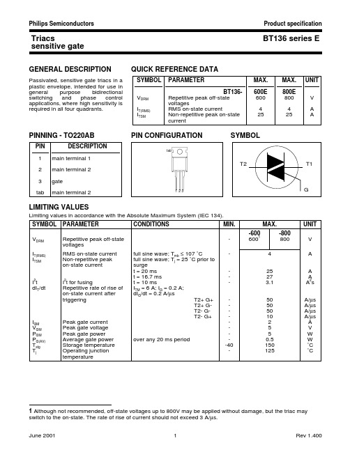
PINNING - TO220AB
PIN CONFIGURATION
SYMBOL
PIN
DESCRIPTION
tab
1 main terminal 1
2 main terminal 2
T2
T1
3 gate
1000 ITSM / A
BBTT113377 IT
ITSM
time
Tj initial = 25 C max
100 dIT/dt limit
T2- G+ quadrant
10 10us
100us
1ms T/s
10ms
100ms
Fig.2. Maximum permissible non-repetitive peak on-state current ITSM, versus pulse width tp, for sinusoidal currents, tp ≤ 20ms.
2.0 2.4
-
UNIT
K/W K/W K/W
STATIC CHARACTERISTICS
Tj = 25 ˚C unless otherwise stated SYMBOL PARAMETER
IGT
Gate trigger current
IL
Latching current
IH
Holding current
surge
t = 20 ms
-
t = 16.7 ms
-
I2t for fusing
t = 10 ms
-
Repetitive rate of rise of ITM = 12 A; IG = 0.2 A;
on-state current after
dIG/dt = 0.2 A/µs
triggering
T2+ G+
-
T2+ G-
-
T2- G-
-
T2- G+
-
Peak gate current
-
Peak gate voltage
-
Peak gate power
-
Average gate power
over any 20 ms period
-
Storage temperature
-40
Operating junction
元器件交易网
Philips Semiconductors
Triacs sensitive gate
Product specification
BT137 series E
GENERAL DESCRIPTION
Glass passivated, sensitive gate triacs in a plastic envelope, intended for use in general purpose bidirectional switching and phase control applications, where high sensitivity is required in all four quadrants.
0
-50
0
50
100
150
Tj / C
Fig.9. Normalised holding current IH(Tj)/ IH(25˚C), versus junction temperature Tj.
25 IT / A Tj = 125 C Tj = 25 C
20
Vo = 1.264 V Rs = 0.0378 Ohms
25 IT(RMS) / A
BT137
20
15
10
5
0
0.01
0.1
1
10
surge duration / s
Fig.5. Maximum permissible repetitive rms on-state current IT(RMS), versus surge duration, for sinusoidal