MTJ-88GX1-FSB-PG中文资料
XGK-CPU 用户手册

如果在安装的环境中有大量的震动出现,请不要让PLC直 接的承受震动,否则,将会引起触电,火灾或者导致系统 不正常的运行.
不要让任何外部的金属碎末进入到产品的内部,这将会引 起触电,火灾或者不正常的运行.
第三章 综合规格 .......................................................................................................................................................................................................................... 3-1
注意
应当在符合PLC手册或者在标准的环境下使用PLC系统, 否则的话,这将会引起的触电,火灾,不正常的运行或者 引起电弧 .
在安装模块之前,请确保PLC的供应电源已经关闭,否则, 这将会引起触电或者导致产品的损坏。
请确保PLC系统中的每一个模块都是正确的安装,如果模 块的安装出现松动或者不正确的现象,这将会引起不正常 的运行,错误或者模块掉下.
在安装接线的时候请确保终端块上的所有螺丝都已经拧紧, 如果终端块上的螺丝有松动,这将会引起触电,火灾或者 导致系统的不正常运行.
* 请确保FG接线端子上使用3级接地方式,这是使用PLC的 基本要求,如果端子上的接地不正确,这将会导致系统的 不正常运行.
在接线的过程中不要让任何外部的金属碎末和线头进入到 产品的内部,否则这将会引起火灾,产品的损坏或者系统 的不正常运行.
Richtek RT7313GS PFC控制器商品说明书

RT7313GSRT7313Copyright © 2016 Richtek Technology Corporation. All rights reserved. is a registered trademark of Richtek Technology Corporation.DS7313-01 July 20161PFC Controller with Critical Conduction ModeGeneral DescriptionThe RT7313 is an active Power Factor Correction (PFC) controller with critical conduction mode (CRM) operation that is designed to meet line current harmonic regulations for the applications of AC/DC adapters, electronic ballasts and medium off-line power converters (<300W). The CRM and Feed-Forward schemes provide near unity power factor across a wide range of input voltages and output powers.The totem-pole gate driver with 600mA sourcing current and 800mA sinking current provides powerful driving capability for power MOSFET to improve conversion efficiency. The RT7313 features an extra low start-up current (≤20μA) and supports a disable function to reduce power consumption in standby mode, which makes it easy to comply with energy saving regulations such as Blue Angel, Energy Star and Energy 2000.This controller integrates comprehensive safety protection functions for robust designs including input under-voltage lockout, output over-voltage protection, under-voltage protection and cycle-by-cycle current limit.The RT7313 is a cost-effective solution for PFC power converter with minimum external components. It is available in the SOP-8 package.Features● Critical Conduction Mode (CRM) Operation ● Constant On-Time Control (Voltage Mode) ● Near Unity Power Factor● Ultra Low Start-up Current (≤20μA)● Input Voltage Feed-Forward Compensation ● Wide Supply Voltage Range from 12V to 25V ● Totem Pole Gate Driver with 600mA/-800mA ● Maximum Frequency Clamping (120kHz) ● DCM THD Optimization ● Fast Dynamic Response● Light Load Burst Mode Operation ● Disable Function● Maximum/Minimum On-Time Limit ● Cycle-by-Cycle Current Limit● Output Over-Voltage Protection (OVP) ● Under-Voltage Lockout (UVLO) ●RoHS Compliant and Halogen FreeApplications● Electrical Lamp Ballast ● LED Lighting●AC/DC Adapter/Charger for Desktop PC, NB, TV, Monitor, Etc.●Entry-Level Server, Web ServerSimplified Application CircuitPSR ConverterOUT +OUT -SSR ConverterOUT +OUT -OUT1OUT2RT7313Copyright © 2016 Richtek Technology Corporation. All rights reserved. is a registered trademark of Richtek Technology Corporation. DS7313-01 July 20162Ordering InformationRT7313G : Green (Halogen Free and Pb Free)Note :Richtek products are :④ RoHScompliant and compatible with the currentrequirements of IPC/JEDEC J-STD-020.④ Suitable for use in SnPb or Pb-free soldering processes.Marking InformationRT7313GS : Product Number YMDNN : Date CodePin Configuration(TOP VIEW)INV COMPFF CSVDD GD ZCDGNDSOP-8Functional Pin DescriptionFunctional Block DiagramRT7313Copyright © 2016 Richtek Technology Corporation. All rights reserved. is a registered trademark of Richtek Technology Corporation.DS7313-01 July 20163OperationCritical Conduction Mode (CRM)The Critical Conduction Mode is also called Transition Mode or Boundary Mode. Figure 1 shows the CRM operating at the boundary between Continuous Conduction Mode (CCM) and Discontinuous Conduction Mode (DCM).In CRM, the power switch turns on immediately when the inductor current decreases to zero. The CRM is the preferred control method for medium power (<300W) applications due to the features of zero current switching and lower peak current than that in DCM.Figure 1. Inductor Current of DCM, CRM and CCM Constant On-Time Voltage Mode ControlFigure 2 shows a typical flyback converter. When the MOSFET turns on with a fixed on-time (t ON ), the inductor current can be calculated by the following equation (1).TX1OUTV OUTFigure 2. Typical flyback ConverterIN L_PK ON PFCVI = t (1)L⨯If the input voltage is a sinusoidal waveform and rectified by a bridge rectifier, the inductor current can be expressed with equation (2). When the converter operates in CRM with constant on-time voltage modecontrol, the envelope of inductor peak current will follow the input voltage waveform with in-phase. The average inductor current will be half of the peak current shown as Figure 3. Therefore, the near unity power factor is easy to be achieved by this control scheme.||||IN_pk ONL_pk PFCV sin θt I sin θ=(2)L ⨯⨯⨯I L_PK I Q1I in_avg I DOUTPeak Inductor Current MOSFET Current Average Input Current Output Diode CurrentV IN Input Voltage V Q1_GATE MOSFET Gate VoltageFigure 3. Inductor Current of CRM with ConstantOn-Time Voltage Mode Control Under-Voltage LockoutThe controller will be enabled when VDD exceeds V ON_TH (16V typ.) and disabled when VDD decreases lower than V OFF_TH (9V typ.).The maximum VDD voltage is set at 27V typically forover-voltage protection shown as Figure 4. An internal 29V zener diode is also used to avoid over voltage stress for the internal circuits.When the VDD is available, the precise reference is generated for internal circuitries such as Error Amplifier, Current Sense, OVP, UVP. The internal reference equips with excellent temperature coefficient performance so that the RT7313 can be operated in varied environments.RT7313Copyright © 2016 Richtek Technology Corporation. All rights reserved. is a registered trademark of Richtek Technology Corporation.DS7313-01 July 20164Figure 4. VDD and UVLOFeedback Voltage DetectionFigure 5 shows the feedback voltage detection circuit. The INV pin is the inverting input of the Error Amplifier with 1.5V reference voltage. Over-voltage protection is provided with threshold voltage 1.65V. If the INV voltage is over 1.65V, the gate driver will be disabled to prevent output over voltage condition or feedback open condition. Although the INV is an input pin with high impedance, it is suggested that the bias current of the potential divider should be over 30µA for noise immunity.Figure 5. Feedback Voltage DetectionTransconductance Error AmplifierThe RT7313 implements transconductance error amplifier with non-linear GM design to regulate the Flyback output voltage and provide fast dynamic response. The transconductance value is 100µA/V in normal operation. When the INV voltage increases over 1.65V or decreases under 1.35V, the output of error amplifier will source or sink 1.5mA(typ.) maximum current at COMP pin respectively shown as Figure 6. Thus, the non-linear GM design can provide fast response for the dynamic load of PFC converters even though the bandwidth of control loop is lower than linefrequency.Figure 6. Non-linear GMFeed-Forward CompensationThe FF pin is an input pin with high impedance to detect the line input voltage shown as Figure 7. A proper voltage divider should be applied to sense the line voltage after bridge diode rectifier. Since the FF voltage is proportional to the line input voltage, it provides a feed-forward signal to compensate the loop bandwidth for high line and low line input conditions.Figure 7. FF Detection CircuitThe constant on-time, t ON , can be derived from the following equations.()2)ON IN_pk ON IN IN_pk L_pk L_pk ONS PFC2IN_pk IN_pk ON ON IN IN_pk ON ON PFC S PFC SIN PFCON IN_pk S V t1P V I I t 4t L V (V t t 11P V t t 4L t 4L t 4P L t (3)t V t =⨯⨯⨯=⨯=⨯⨯⨯⨯=⨯⨯⨯⨯⨯⇒=⎛⎫⨯ ⎪⎝⎭RT7313Copyright © 2016 Richtek Technology Corporation. All rights reserved. is a registered trademark of Richtek Technology Corporation.DS7313-01 July 20165In RT7313, the t ON is implemented by a constant current charging a capacitor till V COMP threshold voltage is reached. Therefore, the t ON is a function of V COMP .()ramp COMP D ON ramp C V V t = 4I ()⨯-Then, the V COMP can be derived from equation (3) and (4).()()()22ramp COMP D IN PFCramp ON IN_pk S ramp IN PFCCOMP D rampON IN_pk S C V V 4P L I t V t I 4P L V + V (5)C t V t ⨯-⨯⨯=⎛⎫⨯ ⎪⎝⎭⨯⨯=⨯⎛⎫⨯ ⎪⎝⎭According to equation (5), the V COMP is reversely proportional to the input voltage so that the V COMP has a large variation for the change of line voltage between high and low input voltages. This variation will impact t ON , Burst mode entry level and loop bandwidth. In order to compensate the variation, the I ramp is designed to be proportional to the input voltage shown as equation (6).()2ONramp IN_pk FF ramp S2ON FF2IN_RMS ramp FF1FF2S 2FF2ramp IN PFC FF1FF2Comp D 2rampt I (V )k V gm t t R = k V gm (6)R + R t V 8gm P L R + R V (FF) + V C π=⨯⨯⨯⎡⎤⎛⎫⨯⨯⨯⎪⎢⎥⎝⎭⎣⎦⎛⎫⨯⨯⨯⨯ ⎪⎝⎭=⨯ (7)in which k, gm ramp , C ramp , and V D are fixed parameters in the RT7313, and the typical values are : k = 0.5, gm ramp = 10μA/V, C ramp = 4.5pF, and V D = 1V. Ramp GeneratorThe RT7313 provides constant on-time voltage mode control to achieve near unity power factor for the CRM Flyback converters. Figure 8 shows the Ramp Generator with Feed-Forward compensation and THD optimization circuit for the constant on-time operation.Figure 8. Ramp GeneratorThe charging current of ramp generator is modulated following the squared FF voltage with line voltage compensation and the THD optimization scheme is implemented to compensate the harmonic distortion. ZCD and Enable FunctionIn CRM operation, when the power switch turns on, the inductor current increases linearly to the peak value. When the power switch turns off, the inductor current decreases linearly to zero. The zero current can be detected by the ZCD pin with the auxiliary winding of Flyback inductor.Figure 9 and Figure 10 show the ZCD block diagram and related waveforms. The ZCD block diagram provides zero current detection, voltage clamp and shutdown control functions. When the inductor current decreases to zero, the auxiliary winding voltage will turn from high to low. Once the ZCD voltage decreases to the threshold V ZCDT (1V, typ.), the controller will generate a signal for gate driver. The hysteresis voltage between the threshold V ZCDA (1.6V, typ.) and V ZCDT is designed to avoid mis-triggering. In order to prevent over voltage stress, the ZCD pin voltage is clamped at V ZCDH (4.8V, typ.) if the input voltage is too high from the auxiliary winding and the ZCD pin voltage is clamped at V ZCDL (0.6V, typ.) if the input voltage is lower than V ZCDL .RT7313Copyright © 2016 Richtek Technology Corporation. All rights reserved. is a registered trademark of Richtek Technology Corporation. DS7313-01 July 20166R ZCDFigure 9.ZCD Block DiagramThe RT7313 provides shutdown function to save power consumption in standby mode. When the ZCD pin is pulled lower than 250mV, the gate driver will be turned off and operate in standby mode with low quiescent current less than 600µA. Once the ZCD pin is released, the controller will be activated.The RT7313 also provides ZCD time-out detection function. If the controller runs at maximum frequency and there is no ZCD signal being detected after 4µs delay time, the PWM will be turned on for ZCD time-out detection.V V I V V V VFigure 10. ZCD Related Waveforms.RT7313Copyright © 2016 Richtek Technology Corporation. All rights reserved. is a registered trademark of Richtek Technology Corporation.DS7313-01 July 20167Absolute Maximum Ratings (Note 1)● Supply Voltage, VDD --------------------------------------------------------------------------------------------- -0.3 to 30V ● Gate Driver Output, GD ------------------------------------------------------------------------------------------ -0.3V to 20V ● Other Pins ----------------------------------------------------------------------------------------------------------- -0.3V to 6V ●Power Dissipation, P D @ T A = 25°CSOP-8 ------------------------------------------------------------------------------------------------------------------ 0.625W ●Package Thermal Resistance (Note 2)SOP-8, θJA ------------------------------------------------------------------------------------------------------------ 160°C/W ● Junction Temperature -------------------------------------------------------------------------------------------- 150°C ● Lead Temperature (Soldering, 10 sec.) ------------------------------------------------------------------------ 260°C● Storage Temperature Range ------------------------------------------------------------------------------------- -65°C to 150°C ● ESD Susceptibility (Note 3)●HBM (Human Body Model) --------------------------------------------------------------------------------------- 2kVRecommended Operating Conditions (Note 4)● Supply Voltage, VDD ----------------------------------------------------------------------------------------------- 12V to 25V ●Junction Temperature Range ------------------------------------------------------------------------------------ -40°C to 125°CElectrical Characteristics(V DD = 15V, T A = 25︒C, unless otherwise specification)RT7313Copyright © 2016 Richtek Technology Corporation. All rights reserved. is a registered trademark of Richtek Technology Corporation. DS7313-01 July 20168Note 1. Stresses beyond those listed “Absolute Maximum Ratings ” may cause permanent damage to the device. These arestress ratings only, and functional operation of the device at these or any other conditions beyond those indicated in the operational sections of the specifications is not implied. Exposure to absolute maximum rating conditions may affect device reliabilityNote 2. θJA is measured under natural convection (still air) at T A = 25︒C with the component mounted on a loweffective-thermal-conductivity single-layer test board on a JEDEC 51-3 thermal measurement standard. θJC is measured at the exposed pad of the package.Note 3. Devices are ESD sensitive. Handling precaution is recommendedNote 4. The device is not guaranteed to function outside its operating conditions. Note 5. Guaranteed by Design.Note 6. Leading edge blanking time and internal propagation delay time is guaranteed by design.RT7313Copyright © 2016 Richtek Technology Corporation. All rights reserved. is a registered trademark of Richtek Technology Corporation.DS7313-01 July 20169Typical Application CircuitTypical PSR Application CircuitOUT +OUT -CTypical SSR Application CircuitOUT +OUT -C OUT1OUT2RT7313Copyright © 2016 Richtek Technology Corporation. All rights reserved. is a registered trademark of Richtek Technology Corporation.DS7313-01 July 201610Typical Operating CharacteristicsNon-inverting Input Reference vs. VDD1.471.481.491.501.511.521.53914192429VDD (V)N o n -i n v e r t i n g R e f e r e n c e (V )Transconduction vs. Temperature889092949698100102-50-25255075100125Temperature (°C)T r a n s c o n d u c t i o n (µA /V )Transconduction vs. Temperature9092949698100102-50-25255075100125Temperature (°C)T r a n s c o n d u c t i o n (µA /V )I COMP vs. V COMP (Sourcing)-2500-2000-1500-1000-50012345V COMP (V)I C O M P(µA ) I COMP vs. V COMP (Sinking)0300600900120015001800012345V COMP (V)I C O MP (µA )Maximum COMP Voltage vs. VDD4.4104.4154.4204.4254.4304.4354.440810.51315.51820.52325.528VDD (V)M a x i m u m C O M P V o l t a g e (V )RT7313Copyright © 2016 Richtek Technology Corporation. All rights reserved. is a registered trademark of Richtek Technology Corporation.DS7313-01 July 201611Maximum COMP Voltage vs. Temperature4.364.374.384.394.404.414.424.43-50-25255075100125Temperature (°C)M a x i m u m C O M P V o l t a g e (V )RT7313Copyright © 2016 Richtek Technology Corporation. All rights reserved. is a registered trademark of Richtek Technology Corporation. DS7313-01 July 201612Application InformationStart-Up Circuit DesignFigure 11. Start-Up CircuitV V IFigure 12. Start-Up Waveforms of VDD and I DD Figure 11 and Figure 12 show the equivalent start-up circuit and VDD waveform during start-up. In general, the start-up time (t start ) is required from system specification. The charging current (Ich VDD ) can be estimated by the following equation.VDD ON_THVDD startC V Ich = (8)t ⨯where C VDD is the capacitor connected between VDD and GND, V ON_TH is the power on threshold (16V typ.). The start-up resistor (R start ) connected between V CSIN and VDD should be able to support the charging current (Ich VDD ), start-up current (I DD_ST ) and leakage current (I leakage ) of C VDD before the VDD is supported by the auxiliary winding. The maximum start-up resistance can be calculated by the equation (9).Start DD_ST VDD leakageRwhere V IN ac_min is the minimum input voltage. Note that the start-up resistor must have adequate voltage rating for reliability. 2 resistors in series can be applied for most of applications.For example, the system required start-up time is 3sec, V IN ac_min = 75V and maximum I DD_ST = 20μA. If C VDD = 22μF is selected and the leakage current of C VDD can be ignored, the start-up resistor should be less than 772k Ω.The capacitor C FF is applied to filter out the input ripplevoltage. The corner frequency should be lower than line frequency (f line ). If the FF pin voltage is not flat, the PF and THD performance will be degraded.line FF1FF2FF1 < 0.1f (10)2(R // R )C π⨯⨯⨯Thermal ConsiderationsFor continuous operation, do not exceed absolutemaximum junction temperature. The maximum power dissipation depends on the thermal resistance of the IC package, PCB layout, rate of surrounding airflow, and difference between junction and ambient temperature. The maximum power dissipation can be calculated by the following formula : P D(MAX) = (T J(MAX) - T A ) / θJAwhere T J(MAX) is the maximum junction temperature, T A is the ambient temperature, and θJA is the junction to ambient thermal resistance.For recommended operating condition specifications, the maximum junction temperature is 125︒C. The junction to ambient thermal resistance, θJA , is layout dependent. For SOP-8 package, the thermal resistance, θJA , is 160︒C/W on a standard JEDEC 51-3 single-layer thermal test board. The maximum power dissipation at T A = 25︒C can be calculated by the following formula :P D(MAX) = (125︒C - 25︒C) / (160︒C/W) = 0.625W for SOP-8 packageThe maximum power dissipation depends on the operating ambient temperature for fixed T J(MAX) and thermal resistance, θJA . The derating curve in FigureRT7313Copyright © 2016 Richtek Technology Corporation. All rights reserved. is a registered trademark of Richtek Technology Corporation.DS7313-01 July 20161313 allows the designer to see the effect of rising ambient temperature on the maximum power dissipation.Figure 13. Derating Curve of Maximum PowerDissipation Layout ConsiderationsA proper PCB layout can abate unknown noise interference and EMI issue in the switching power supply. Please refer to the guidelines when designing a PCB layout for switching power supply.④The current path(1) from input capacitor, transformer, MOSFET, R CS return to input capacitor is a high frequency current loop. The path(2) from GD pin,MOSFET, R CS return to input capacitor is also a high frequency current loop. They must be as short as possible to decrease noise coupling and kept a space to other low voltage traces, such as IC control circuit paths, especially. Besides, the path(3) between MOSFET ground(b) and IC ground(d) is recommended to be as short as possible, too.④It is good for reducing noise, output ripple and EMI issue to separate ground traces of input capacitor(a), MOSFET(b), auxiliary winding(c) and IC control circuit(d). Finally, connect them together on input capacitor ground(a). The areas of these ground traces should be kept large.④Placing bypass capacitor for abating noise on IC is highly recommended. The capacitors C INV and C CS should be placed as close to controller as possible. ④In addition, apply sufficient copper area at the anode and cathode terminal of the diode for heat-sinking. It is recommended to apply a larger area at the quiet cathode terminal. A large anode area will induce high-frequency radiated EMI.NeutralFigure 14. PCB Layout GuideRT7313Copyright © 2016 Richtek Technology Corporation. All rights reserved. is a registered trademark of Richtek Technology Corporation. DS7313-01 July 201614Outline Dimension8-Lead SOP Plastic PackageRichtek Technology Corporation14F, No. 8, Tai Yuen 1st Street, Chupei City Hsinchu, Taiwan, R.O.C. Tel: (8863)5526789Richtek products are sold by description only. Richtek reserves the right to change the circuitry and/or specifications without notice at any time. Customers should obtain the latest relevant information and data sheets before placing orders and should verify that such information is current and complete. Richtek cannot assume responsibility for use of any circuitry other than circuitry entirely embodied in a Richtek product. Information furnished by Richtek is believed to be accurate and reliable. However, no responsibility is assumed by Richtek or its subsidiaries for its use; nor for any infringements of patents or other rights of third parties which may result from its use. No license is granted by implication or otherwise under any patent or patent rights of Richtek or its subsidiaries.RT7313GS。
贴片开关二极管型号 MMBD7000LT1G BAS16WT1G BAV99WT1G 贴片低压差稳压器 MC33269DT-3.3G TL431ACLPG

贴片开关二极管型号MMSD4148T1G MMBD7000LT1G BAS16WT1G BAV99WT1G 贴片低压差稳压器MC33269DT-3.3G TL431ACLPG深圳市金色长城科技有限公司是一家集渠道代理与分销的专业化半导体公司,产品信息网络资源丰富,战略合作遍布全球。
主要供应于通讯,电源。
安防,汽车电子,工业控制,物联网,新能源,智能家居,智慧家庭等专业领域,诚实经营,务实进取。
为AI智能世界提供安全互联的解决方案!拥有务实高效的金牌团队及完善的配套服务从而促进了供求关系的平衡,满足了生产厂商的采购需求!金色长城,赢在品牌战略!整合优质资源!形成优势互补!达成财富共享!公司产品品种规格齐全,有普通整流、快速恢复、高效率、超快速和肖特基等各种系列与多种封装形式的二极管。
产品介绍贴片二极管又称晶体二极管,简称二极管(diode),另外,还有早期的真空电子二极管;它是一种具有单向传导电流的电子器件。
在半导体二极管内部有一个PN结两个引线端子,这种电子器件按照外加电压的方向,具备单向电流的转导性。
一般来讲,贴片晶体二极管是一个由p型半导体和n型半导体烧结形成的p-n结界面。
在其界面的两侧形成空间电荷层,构成自建电场。
当外加电压等于零时,由于p-n 结两边载流子的浓度差引起扩散电流和由自建电场引起的漂移电流相等而处于电平衡状态,这也是常态下的二极管特性。
具体参数贴片二极管的管压降:硅二极管(不发光类型)正向管压降0.7V,锗管正向管压降为0.3V,发光二极管正向管压降会随不同发光颜色而不同。
主要有三种颜色,具体压降参考值如下:红色发光二极管的压降为2.0--2.2V,黄色发光二极管的压降为1.8—2.0V,绿色发光二极管的压降为3.0—3.2V,正常发光时的额定电流约为20mA。
贴片二极管的电压与电流不是线性关系,所以在将不同的贴片二极管并联的时候要接相适应的电阻。
贴片二极管特性贴片二极管(英语:Diode),电子元件当中,一种具有两个电极的装置,只允许电流由单一方向流过。
浙江航芯源集成电路科技有限公司C49009RH产品手册说明书

浙江航芯源集成电路科技有限公司浙江航芯源集成电路科技有限公司Zhejiang HangXinYuan IC Technology Co.,LtdC49009RH 产品手册3路小电流漏极调制&栅压调节&可驱动外置pmos抗辐射TR 电源管理芯片1.产品特性➢8V PA 发射电源调制:8V/800mA ➢5V PA 发射电源调制:5V/200mA ➢LNA 接收电源调制:5V/200mA ➢GaAs 栅压调节范围:-0.3V~-1.05V➢GaAs 栅极驱动电流:±2mA➢DRV_PA 可驱动外接pmos➢集成正/负压欠压锁定➢过脉宽保护功能。
➢0/-5V 开关控制➢总剂量(TID )耐受:≥100k rad(si)➢单粒子锁定及烧毁对线性能量传输(LET )的抗干扰度:≥75MeV*cm 2/mg2.功能描述T/R 电源管理芯片C49009RH 包含漏极调制、栅极调制、脉宽保护、开关控制等功能模块。
其中发射信号具有5V 和8V 两路,发射、接收漏极调制信号可以通过T 和R 输入引脚配置输出各800mA/200mA/200mA电流,芯片配有DRV_PA 引脚可实现外接pmos 扩流使用。
芯片栅极调制电压为-0.3V~-1.05V ,输出电流±2mA 可通过EN 夹断。
3.产品应用➢GaAs FET 供电➢栅极调制驱动4.裸芯片简介本产品为裸芯片,尺寸为2600μm* 2000μm (不包含划片槽)江航芯源集成电路科技有限5. 绝对最大额定值表 1 绝对最大额定值(1)使用中超过这些绝对最大值可能对芯片造成永久损坏。
6. 推荐工作条件1) PA 电源V T :8V 2) 正电源V CC :5V3) 负压电源V EE :-5V4) 工作环境温度T A :-55℃~125℃ 5) 贮存温度T STG :-65℃~150℃7. 主要电参数、除非特别说明,V T =8V ,VCC=5V ,T A = -55℃~125℃表 2 主要电参数浙江航技有8. 功能框图及引脚介绍8.1 功能框图VG TXOENGND VEEPA_VDDRV_PA SWA SWB图 1 C49009RH 功能框图科技有限公司8.2 引脚介绍229439762110789714311591图 2 引脚分布图➢ 芯片尺寸:2650μm * 2050μm (包含划片槽尺寸) ➢ PAD 尺寸: VG 、TXO 、RXO :100μm * 250μmVT 、PA_VD :100μm * 430μm其它PAD :100μm * 100μm表 3 引脚介绍有限公司9. 逻辑功能说明下列各表给出C49009RH 应用时的漏极和栅极调制真值表表 4 栅极调制状态真值表表 5 栅压调节真值表浙集成电路科技有表 6 漏极调制逻辑真值表表 7 开关控制逻辑真值表➢ “1”指3.3V/5V ➢ T 、R 、EN 、VG_SEL<3:0>均有1MΩ电阻下拉。
T8XX-XXXG中文资料

®1/11Table 1: Main FeaturesDESCRIPTIONAvailable either in through-hole or surface-mount packages, the BTA08, BTB08 and T8 triac series is suitable for general purpose AC switching. They can be used as an ON/OFF function in applica-tions such as static relays, heating regulation, in-duction motor starting circuits... or for phase control operation in light dimmers, motor speed controllers,...The snubberless versions (BTA/BTB...W and T8series) are specially recommended for use on inductive loads, thanks to their high commutation performances.Logic level versions are designed to interface directly with low power drivers such as microcontrollers.By using an internal ceramic pad, the BTA series provides voltage insulated tab (rated at 2500V RMS ) complying with UL standards (file ref.:E81734).Symbol Value Unit I T(RMS)8A V DRM /V RRM 600 and 800V I GT (Q 1)5 to 50mABTA08, BTB08 and T8 Series8A TRIAC SREV. 6February 2006SNUBBERLESS™, LOGIC LEVEL & STANDARDTable 2: Order CodesPart Number Marking BTA08-xxxxxRG See page table 8 onpage 10BTB08-xxxxxRG T8xx-xxxG T8xx-xxxH T8xx-xxxBBTA08, BTB08 and T8 Series2/11Table 3: Absolute Maximum Ratings Tables 4: Electrical Characteristics (T j = 25°C, unless otherwise specified)■SNUBBERLESS and Logic Level (3 quadrants)Symbol ParameterValue Unit I T(RMS)RMS on-state current (full sine wave)IPAK/D 2PAK/DPAK/TO-220AB T c = 110°C 8ATO-220AB Ins.T c = 100°C I TSM Non repetitive surge peak on-state current (full cycle, T j initial = 25°C) F = 50 Hz t = 20 ms 80A F = 60 Hz t = 16.7 ms84I ²t I ²t Value for fusingt p = 10 ms 36A ²s dI/dt Critical rate of rise of on-state cur-rent I G = 2 x I GT , t r ≤ 100 ns F = 120 Hz T j = 125°C 50A/µs I GM Peak gate currentt p = 20 µsT j = 125°C 4A P G(AV)Average gate power dissipation T j = 125°C1W T stg T jStorage junction temperature rangeOperating junction temperature range- 40 to + 150- 40 to + 125°CSymbol Test ConditionsQuad-rantT8BTA08 / BTB08Unit T810T835TW SW CW BW I GT (1)V D = 12 V R L = 30 ΩI - II -III MAX.10355103550mA V GT I - II - III MAX.1.3V V GD V D = V DRM R L = 3.3 k ΩT j = 125°C I - II - IIIMIN.0.2V I H (2)I T = 100 mA MAX.153510153550mA I L I G = 1.2 I GTI - III MAX.255010255070mAII306015306080dV/dt (2)V D = 67 %V DRM gate open T j = 125°CMIN.4040020404001000V/µs (dI/dt)c (2)(dV/dt)c = 0.1 V/µs T j = 125°CMIN.5.4- 3.5 5.4--A/ms(dV/dt)c = 10 V/µs T j = 125°C2.8- 1.5 2.98--Without snubber T j = 125°C- 4.5-- 4.57BTA08, BTB08 and T8 Series3/11■Standard (4 quadrants)Table 5: Static Characteristics Table 6: Thermal resistance Symbol Test ConditionsQuadrant BTA08 / BTB08Unit C B I GT (1)V D = 12 V R L = 30 ΩI - II - III IV MAX.255050100mA V GT ALL MAX. 1.3V V GD V D = V DRM R L = 3.3 k Ω T j = 125°C ALLMIN.0.2V I H (2)I T = 500 mA MAX.2550mA I L I G = 1.2 I GTI - III - IVMAX.4050mA II80100dV/dt (2)V D = 67 %V DRM gate open T j = 125°CMIN.200400V/µs (dV/dt)c (2)(dI/dt)c = 5.3 A/ms T j = 125°C MIN.510V/µsSymbol Test ConditionsValueUnit V T (2)I TM = 11 A t p = 380 µs T j = 25°C MAX. 1.55V V to (2)Threshold voltage T j = 125°C MAX.0.85V R d (2)Dynamic resistance T j = 125°C MAX.50m ΩI DRM I RRMV DRM = V RRMT j = 25°C MAX.5µA T j = 125°C1mANote 1: minimum I GT is guaranted at 5% of I GT max.Note 2: for both polarities of A2 referenced to A1.Symbol ParameterValue Unit R th(j-c)Junction to case (AC)IPAK / D 2PAK / DPAK / TO-220AB 1.6°C/WTO-220AB Insulated 2.5R th(j-a)Junction to ambientS = 1 cm ²D 2PAK 45°C/WS = 0.5 cm ²DPAK70TO-220AB / TO-220AB Insulated 60IPAK100S = Copper surface under tab.BTA08, BTB08 and T8 Series4/11Figure 1: Maximum power dissipation versus RMS on-state current (full cycle)Figure 2: RMS on-state current versus case temperature (full cycle)Figure 3: RMS on-state current versus ambient temperature (printed circuit board FR4, copper thickness: 35µm) (full cycle)Figure 4: Relative variation of thermal impedance versus pulse durationFigure 5: On-state characteristics (maximum values)Figure 6: Surge peak on-state current versus number of cyclesBTA08, BTB08 and T8 Series5/11Figure 7: Non-repetitive surge peak on-state current for a sinusoidal pulse with width t p < 10 ms and corresponding value of I 2tFigure 8: Relative variation of gate trigger current, holding current and latching current versus junction temperature (typical values)Figure 9: Relative variation of critical rate of decrease of main current versus (dV/dt)c (typical values) (Snubberless & L ogic level types)Figure 10: Relative variation of critical rate of decrease of main current versus (dV/dt)c (typical values) (Standard types)Figure 11: Relative variation of critical rate of decrease of main current versus junction temperatureFigure 12: DPAK and D 2P AK Thermal resistance junction to ambient versus copper surface under tab (printed circuit board FR4, copper thickness:35µm)BTA08, BTB08 and T8 Series6/11Figure 13: Ordering Information Scheme (BTA08 and BTB08 series)Figure 14: Ordering Information Scheme (T8 series)Table 7: Product SelectorPart NumberVoltage (xxx)Sensitivity Type Package 600 V 800 V BTA/BTB08-xxxB X X 50 mA Standard TO-220AB BTA/BTB08-xxxBW X X 50 mA Snubberless TO-220AB BTA/BTB08-xxxC X X 25 mAStandard TO-220AB BTA/BTB08-xxxCW X X 35 mA Snubberless TO-220AB BTA/BTB08-xxxSW X X 10 mA Logic level TO-220AB BTA/BTB08-xxxTW X X 5 mA Logic Level TO-220AB T810-xxxG X X 10 mA Logic Level D2PAK T810-xxxH X X 10 mA Logic Level IPAK T835-xxxB X X 35 mA Snubberless DPAK T835-xxxG X X 35 mA Snubberless D 2PAK T835-xxxHXX35 mASnubberlessIPAKBTB: non insulated TO-220AB packageBTA08, BTB08 and T8 Series Figure 15: D2PAK Package Mechanical DataFigure 16: D2PAK Foot Print Dimensions(in millimeters)7/11BTA08, BTB08 and T8 SeriesFigure 17: DPAK Package Mechanical DataFigure 18: DPAK Foot Print Dimensions (in millimeters)8/11BTA08, BTB08 and T8 Series9/11BTA08, BTB08 and T8 Series10/11In order to meet environmental requirements, ST offers these devices in ECOPACK® packages. These packages have a Lead-free second level interconnect . The category of second level interconnect is marked on the package and on the inner box label, in compliance with JEDEC Standard JESD97. The maximum ratings related to soldering conditions are also marked on the inner box label. ECOPACK is an ST trademark. ECOPACK specifications are available at: .Table 8: Ordering InformationOrdering type Marking Package Weight Base qtyDelivery modeBTA/BTB08-xxxyzRGBTA/BTB08-xxxyzTO-220AB 2.3 g 50Tube T8yy-xxxG T8yyxx D 2PAK 1.5 g 50Tube T8yy-xxxG-TR T8yyxx 1000Tape & reel T8yy-xxxB T8yyxx DPAK 0.3 g 75Tube T8yy-xxxB-TR T8yyxx 2500Tape & reel T8yy-xxxHT8yyxxIPAK0.4 g75TubeNote: xxx = voltage, yy = sensitivity, z = typeTable 9: Revision HistoryDate Revision Description of ChangesApr-20025A Last update.13-Feb-20066TO-220AB delivery mode changed from bulk to tube.ECOPACK statement added.元器件交易网BTA08, BTB08 and T8 Series Information furnished is believed to be accurate and reliable. However, STMicroelectronics assumes no responsibility for the consequencesof use of such information nor for any infringement of patents or other rights of third parties which may result from its use. No license is grantedby implication or otherwise under any patent or patent rights of STMicroelectronics. Specifications mentioned in this publication are subjectto change without notice. This publication supersedes and replaces all information previously supplied. STMicroelectronics products are notauthorized for use as critical components in life support devices or systems without express written approval of STMicroelectronics.The ST logo is a registered trademark of STMicroelectronics.All other names are the property of their respective owners© 2006 STMicroelectronics - All rights reservedSTMicroelectronics group of companiesAustralia - Belgium - Brazil - Canada - China - Czech Republic - Finland - France - Germany - Hong Kong - India - Israel - Italy - Japan - Malaysia - Malta - Morocco - Singapore - Spain - Sweden - Switzerland - United Kingdom - United States of America11/11。
大容量NANDFlash在嵌入式系统中的应用

・计算机应用・大容量NAND Flash 在嵌入式系统中的应用汉泽西 吕 飞(西安石油大学电子工程学院 陕西西安)摘 要:文章以主要用于手机领域的Samsung NAND Flash 器件K 9K 1G 08U0B -J I B0为例,对比了NAND 和NOR Flash 的异同,阐述了NAND Flash 的基本结构和使用方法,介绍了大容量NAND Flash 在嵌入式系统中的应用,以及如何在Linux 操作系统中设置对NAND Flash 的支持。
关键词:嵌入式系统;NAND Flash ;K 9K 1G 08U0B -J I B0;Linux中图法分类号:TP333 文献标识码:B 文章编号:100429134(2006)01200622030 引 言在嵌入式市场日益广泛的今天,即将组建的3G网络和多媒体革命将进一步推动移动存储市场的发展。
更多的图片、视频、音乐、3D 游戏、电子地图等在手机、PDA 、MP3、数码相机中的出现,已使得现有设备的存储容量应接不暇。
扩大存储容量,成为各类产品制造商追捧的重点。
在上述各种移动终端设备中,手机占据着核心位置,对存储器的要求也最为严格。
三年前,2MB ~4MB 是手机的存储容量标准,存储器主要使用读取功能,而NOR +SRAM 的结合也是当时唯一的选择。
与此相比,现在的手机中存储了更多的多媒体内容,64MB ~128MB 的存储容量成为标准配置,写性能变得更为重要。
短短3年,在向多媒体平台演变的过程中,手机的存储容量增长了15倍。
继2004年照相功能使手机容量大幅度提升后,音乐功能也将在未来加快存储容量增长的步伐。
所有这些情况都表明了大容量的Nand Flash 会发挥越来越大的作用。
1 NAND 和NO R flash现在的flash memory 主要包括以下两大类:针对程序和数据存储的NOR flash ;针对大容量存储的NAND flash 。
GFSIGNET8850-1电导型变送器说明书讲解
+GF+SIGNET 8850-1 电导型变送器说明书注意目录● 在输入输出接 1. 安装线前切断电源。
2. 技术性能● 认真地根据指 3. 电路连接导以避免个人伤害。
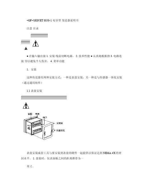
4. 菜单功能1.安装这种传送器有两种安装方式:一种是表盘安装,另一种是与传感器一体化安装(通过通用组件)1.1 表盘安装表盘安装成套工具与要安装到表盘的硬件一起提供以保证达到NEMA 4X的密封水平。
1. 盘装时,仪表面板之间的距离推荐为一英寸。
2. 将垫片装在仪表上,然后装盘。
3. 安装架从仪表背部装入,滑动到锁定位置。
4. 接线到端子。
5. 需要取下仪表时,用带子从前面固定仪表或从背部用手抓住仪表。
不要放开。
压下快速锁定装置,取出仪表。
1. 2通用组件(3-8050)1.安装变送器板。
2.接线到端子。
3.用压旋装置固定,密封出线口。
2.技术指标概述兼容电极:+GF+SIGNET 3-28XX-1 标准系列电导精确度:±2% 读取误差外壳:● 防护等级:NEMA 4X/IP65 ● 壳体材料:PBT● 显示窗:聚氨酯● 键盘:密封4键硅橡胶● 重量:325克显示:● 2*16LCD● 对比度:用户可选择,5级● 刷新周期:1秒环境环境温度:-10到70C(14到158F 存储温度:-15到8OC(5到176F 相对湿度:0到95%,无浓缩标准● CSA,CE,UL● ISO9001标准下制造美国专利号#5,708,363 电气特性传感器输入范围:● 传导率:0。
055到400,000微秒● 阻抗:10-18.26千欧● TDS :0.023-2000,000PPM电气特性传感器输入范围:● 传导率:0。
055到400,000微秒● 阻抗:10-18.26千欧● TDS :0.023-2000,000PPM ● 温度:PT1000, -25到120C (-13-248F )电流输出:● 4到20mA 隔离,完全可调和可逆输出● 电源:12到24VDC ±5% 稳压● 最大闭环阻抗:50欧姆 MAX @12V, 325欧姆 MAX @18V, 600欧姆MAX @ 24V ● 刷新周期:0.5秒● 精确度:±0.03mA@ 25C,24V集电极开路输出:高,低,可编程脉冲● 集电极,隔离,50mA 吸入或源电流,30VDC max拉入电压● 滞后:用户可调3.电气连接注意:在拆除电线前没有完全打开端子接线夹可能导致仪表的永久损坏。
K9F2G08U0M中文资料

2
元器件交易网
K9F2G08Q0M K9F2G16Q0M K9F2G08U0M K9F2G16U0M
Preliminary FLASH MEMORY
256M x 8 Bit / 128M x 16 Bit NAND Flash Memory
PRODUCT LIST
Part Number K9F2G08Q0M-Y,P K9F2G16Q0M-Y,P K9F2G08U0M-Y,P K9F2G16U0M-Y,P 2.7 ~ 3.6V Vcc Range 1.70 ~ 1.95V Organization X8 X16 X8 X16 TSOP1 PKG Type
FEATURES
• Voltage Supply -1.8V device(K9F2GXXQ0M): 1.70V~1.95V -3.3V device(K9F2GXXU0M): 2.7 V ~3.6 V • Organization - Memory Cell Array -X8 device(K9F2G08X0M) : (256M + 8,192K)bit x 8bit -X16 device(K9F2G16X0M) : (128M + 4,096K)bit x 16bit - Data Register -X8 device(K9F2G08X0M): (2K + 64)bit x8bit -X16 device(K9F2G16X0M): (1K + 32)bit x16bit - Cache Register -X8 device(K9F2G08X0M) : (2K + 64)bit x8bit -X16 device(K9F2G16X0M) : (1K + 32)bit x16bit • Automatic Program and Erase - Page Program -X8 device(K9F2G08X0M) : (2K + 64)Byte -X16 device(K9F2G16X0M) : (1K + 32)Word - Block Erase -X8 device(K9F2G08X0M) : (128K + 4K)Byte -X16 device(K9F2G16X0M) : (64K + 2K)Word • Page Read Operation - Page Size - X8 device(K9F2G08X0M) : 2K-Byte - X16 device(K9F2G16X0M) : 1K-Word - Random Read : 25µs(Max.) - Serial Access : 50ns(Min.) 30ns(Min., K9F2G08U0M only) • Fast Write Cycle Time - Page Program time : 300µs(Typ.) - Block Erase Time : 2ms(Typ.) • Command/Address/Data Multiplexed I/O Port • Hardware Data Protection - Program/Erase Lockout During Power Transitions • Reliable CMOS Floating-Gate Technology - Endurance : 100K Program/Erase Cycles - Data Retention : 10 Years • Command Register Operation • Cache Program Operation for High Performance Program • Power-On Auto-Read Operation • Intelligent Copy-Back Operation • Unique ID for Copyright Protection • Package : - K9F2GXXX0M-YCB0/YIB0 48 - Pin TSOP I (12 x 20 / 0.5 mm pitch) - K9F2GXXX0M-PCB0/PIB0 : Pb-FREE PACKAGE 48 - Pin TSOP I (12 x 20 / 0.5 mm pitch)