ADR520ARTZ-REEL7中文资料
AD5320中文资料
a
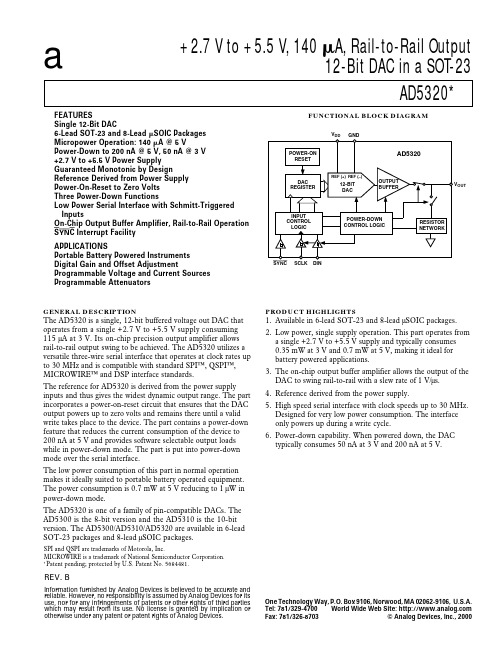
+2.7 V to +5.5 V, 140 A, Rail-to-Rail Output 12-Bit DAC in a SOT-23 AD5320*
FUNCTIONAL BLOCK DIAGRAM
VDD GND POWER-ON RESET
FEATURES Single 12-Bit DAC 6-Lead SOT-23 and 8-Lead SOIC Packages Micropower Operation: 140 A @ 5 V Power-Down to 200 nA @ 5 V, 50 nA @ 3 V +2.7 V to +5.5 V Power Supply Guaranteed Monotonic by Design Reference Derived from Power Supply Power-On-Reset to Zero Volts Three Power-Down Functions Low Power Serial Interface with Schmitt-Triggered Inputs On-Chip Output Buffer Amplifier, Rail-to-Rail Operation SYNC Interrupt Facility APPLICATIONS Portable Battery Powered Instruments Digital Gain and Offset Adjustment Programmable Voltage and Current Sources Programmable Attenuators
VDD 10
1/4 Scale to 3/4 Scale Change (400 Hex to C00 Hex). RL = 2 kΩ; 0 pF < CL < 200 pF. See Figure 16. RL = 2 kΩ; CL = 500 pF RL = ∞ RL = 2 k Ω 1 LSB Change Around Major Carry. See Figure 19.
ADI中文版数据手册说明书
ADI 中文版数据手册是英文版数据手册的译文,敬请谅解翻译中可能存在的语言组织或翻译错误,ADI 不对翻译中存在的差异或由此产生的错误负责。
如需确认任何词语的准确性,请参考ADI 提供的最新英文版数据手册。
消除影响JESD204B 链路传输的因素作者:Ian Beavers ,ADI 公司应用工程师JESD204B 串行数据链路接口针对支持更高速转换器不断增长的带宽需求而开发。
作为第三代标准,它提供更高的通道速率最大值(每通道高达12.5 Gbps),支持确定延迟和谐波帧时钟。
此外,得益于转换器性能的提升——这些转换器兼容开放市场FPGA 解决方案,并且可扩展——现已能轻松传输大量待处理的数据。
FPGA 供应商已讨论了许多年有关千兆串行/解串(SERDES)接口的话题,虽然过去大部分模数转换器(ADC)和数模转换器(DAC)并未配备这类高速串行接口。
FPGA 和转换器不与任何通用标准接口,无法利用SERDES 的高带宽。
JESD204B 兼容型转换器能够解决这个问题,而人们针对这种新功能提出了一些问题。
什么是8b/10b 编码,为什么JESD204B 接口需使用这种编码?无法确保差分通道上的直流平衡信号不受随机非编码串行数据干扰,因为很有可能会传输大量相反的1或0数据。
通过串行链路传输的随机数据还可能长时间无活动状态,并在相对较长的时间内为全1或全0。
发生这种情况时,未编码串行数据流的直流平衡被隔离,产生两种极端情况中的一种。
此时,若链路上再次传输有效数据,则很有可能发生位错误,因为线路重新开始偏置。
另外,一个长期的问题是电子迁移,因为相对差分对的另一侧,会保持一侧的差分直流电压。
为了克服这些问题,通常在差分串行数据流中(包括JESD204B)采用8b/10b 编码方案。
8b/10b 编码采用10个数据位,通过查找表方式从源端发送器发送8位初始信息。
这种方式具有25%的固有开销(10b/8b = 1.25),效率较低。
AD8027中文资料

10 +VS
– + – +
9 8 7 6
VOUTB –IN B +IN B DISABLE/SELECT B
图1 连接图(顶视图)
关断模式
无反相:VIN > |VS| + 200 mV 宽电源电压范围:2.7V至12 V 小型封装:SOIC-8、SOT-23-6、MSOP-10
ADI中文版数据手册是英文版数据手册的译文,敬请谅解翻译中可能存在的语言组织或翻译错误,ADI不对翻译中存在的差异或由此产生的错误负责。如需确认任何词语的准确性,请参考ADI提供 的最新英文版数据手册。
AD8027/AD8028
目录
技术规格 ........................................................................................... 3 绝对最大额定值.............................................................................. 6 最大功耗...................................................................................... 6 ESD警告....................................................................................... 6 典型工作特性 .................................................................................. 8 工作原理.................................................................................... 17 输入级 ........................................................................................ 17 交越选择.................................................................................... 17 输出级 ........................................................................................ 18 直流误差.................................................................................... 18 宽带运作 ......................................................................................... 19 电路考虑.................................................................................... 19 应用.................................................................................................. 21 使用SELECT引脚..................................................................... 21 驱动16位ADC........................................................................... 21 带通滤波器 ............................................................................... 22 设计工具和技术支持.............................................................. 22 外形尺寸 ......................................................................................... 23 订购指南.................................................................................... 24
OP07C中文资料

OP07C中文资料一、Op07芯片是一种低噪声,非斩波稳零的单运算放大器集成电路。
由于OP07具有非常低的输入失调电压(对于OP07A最大为25μV),所以OP07在很多应用场合不需要额外的调零措施。
OP07同时具有输入偏置电流低(OP07A为±2nA)和开环增益高(对于OP07A 为300V/mV)的特点,这种低失调、高开环增益的特性使得OP07特别适用于高增益的测量设备和放大传感器的微弱信号等方面。
二、OP07特点:超低偏移: 150μV最大。
低输入偏置电流: 1.8nA 。
低失调电压漂移: 0.5μV/℃。
超稳定,时间: 2μV/month最大高电源电压范围:±3V至±22V三、OP07内部结构原理图四、OP07芯片引脚功能说明:1和8为偏置平衡(调零端),2为反向输入端,3为正向输入端,4接地,5空脚 6为输出,7接电源+ABSOLUTE MAXIMUM RATINGS 最大额定值五、OP07典型应用电路图4 输入失调电压调零电路图5 典型的偏置电压试验电路图6 老化电路图7 典型的低频噪声放大电路图8 高速综合放大器图9 选择偏移零电路图10 调整精度放大器图11高稳定性的热电偶放大器图12 精密绝对值电路op07的功能介绍:Op07芯片是一种低噪声,非斩波稳零的双极性运算放大器集成电路。
由于OP07具有非常低的输入失调电压(对于OP07A 最大为25μV),所以OP07在很多应用场合不需要额外的调零措施。
OP07同时具有输入偏置电流低(OP07A为±2nA)和开环增益高(对于OP07A为300V/mV)的特点,这种低失调、高开环增益的特性使得OP07特别适用于高增益的测量设备和放大传感器的微弱信号等方面。
特点:超低偏移: 150μV最大。
低输入偏置电流: 1.8nA 。
低失调电压漂移: 0.5μV/℃。
超稳定,时间: 2μV/month最大高电源电压范围:±3V至±22V工作电源电压范围是±3V~±18V;OP07完全可以用单电源供电,你说的+5V,-5V绝对没有问题,用单+5V也可以供电,但是线性区间太小,单电源供电,模拟地在1/2 VCC. 建议电源最好>8V,否则线性区实在太小,放大倍数无法做大,一不小心,就充顶饱和了。
ADI中文版数据手册说明书

Rev. 0 Document FeedbackInformation furnished by Analog Devices is believed to be accurate and reliable. However , no responsibility is assumed by Analog Devices for its use, nor for any infringements of patents or other rights of third parties that may result from its use. Speci cations subject to change without notice. No license is granted by implication or otherwise under any patent or patent rights of Analog Devices. T rademarks and registered trademarks are the property of their respective owners.One Technology Way, P.O. Box 9106, Norwood, MA 02062-9106, U.S.A.Tel: 781.329.4700 ©2013 Analog Devices, Inc. All rights reserved. Technical Support ADI 中文版数据手册是英文版数据手册的译文,敬请谅解翻译中可能存在的语言组织或翻译错误,ADI 不对翻译中存在的差异或由此产生的错误负责。
如需确认任何词语的准确性,请参考ADI 提供的最新英文版数据手册。
典型应用电路CHANNEL 2BUCK REGULATOR (1.2A/2.5A/4A)CHANNEL 3BUCK REGULATOR(1.2A)OSCILLATOR INT VREG 100mAQ1Q2L1L2VREGSYNC/MODERT FB1BST1SW1DL1PGND DL2SW2BST2FB2L3BST3SW3FB3PGND3L4BST4SW4FB4PGND4VREGPVIN1COMP1EN1PVIN2COMP2EN2PVIN3PWRGD SS34COMP3EN3PVIN4COMP4EN4C2C1C4C3C5C6C7C8C9C10C11C12C134.5V TO 15VVOUT1VOUT2VOUT3VOUT4R ILIM1R ILIM2VREGEXPOSED PADSS12C0VDDCHANNEL 5200mA LDO REGULATORFB5PVIN5EN5VOUT5C14C15VOUT51.7V TO 5.5VADP5052CHANNEL 1BUCK REGULATOR (1.2A/2.5A/4A)CHANNEL 4BUCK REGULATOR(1.2A)10900-001图1.带四通道降压调节器和200 mA LDO 调节器的5通道集成式电源解决方案产品特性宽输入电压范围:4.5 V 至15 V输出精度:±1.5%(整个温度范围内)可调开关频率范围:250 kHz 至1.4 MHz 可调/固定输出选项,可通过工厂熔丝调节电源调节通道1和通道2:带低端FET 驱动器的可编程1.2 A/2.5 A/4 A 同步降压调节器通道3和通道4:1.2 A 同步降压调节器通道5:200 mA 低压差(LDO)调节器针对小负载要求,5.1 V LDO 电源始终处于激活状态8 A 单通道输出(通道1和通道2并联工作)精密使能,0.8 V 精确阈值有源输出放电开关FPWM 或自动PWM/PSM 模式选择频率同步输入或输出针对OVP/OCP 故障提供可选的闩锁保护所选通道的电源良好指示UVLO 、OCP 和TSD 保护48引脚7 mm × 7 mm LFCSP 封装结温范围:−40°C 至+125°C应用小型蜂窝基站FPGA 和处理器应用安防和监控医疗应用概述ADP5052在一个48引脚LFCSP 封装中集成了四个高性能降压调节器和一个200 mA 低压差(LDO)调节器,可满足严苛的性能和电路板空间要求。
7MBP50RJ120中文资料

Ic=25A
Terminal
-Ic=25A
Terminal
Turn-on time
ton
VDC=600V,Tj=125°C
Turn-off time
toff
IC=50A Fig.1, Fig.6
Reverse recovery time
trr
VDC=600V, IF=50A Fig.1, Fig.6
Interval 20s, 10 times
Judge : no over-current, no miss operating
Min. 75 38 150
Typ. -
10 -
Max. Unit
-
A-A来自-µs12
µs
-
°C
-
20
-
°C
110
- 125
°C
-
20
-
°C
11.0
-
12.5 V
0.2
0.5
/ALM
alarm
tALM > Max. 1
tALM > Max. 2
t ALM 2ms(typ.) 3
Fault : Over-current,Over-heat or Under-voltage
Input zener voltage Alarm signal hold time
Limiting Resistor for Alarm
Symbol Iccp ICCN Vin(th)
VZ tALM
RALM
Condition Switching Trequency : 0 to 15kHz Tc=-20 to 125°C Fig.7 ON OFF Rin=20k ohm Tc=-20°C Fig.2 Tc=25°C Fig.2 Tc=125°C Fig.2
V7 DeviceNet 与 ADR 选项套件 CM013 产品说明书

1.Applicable products: Standard V7 drives CIMR-V7AM*) withCommunication specific software installed (not V74X or V7N). Check V7keypad monitor U-10 or the PRG # on the V7 nameplate for version 8340or 8350 software.Note:To order a V7 with Communication specific software, use the following part number format: CIMR-V7AM****1-057.2.When using this Kit, it is strongly recommended that no connections bemade to the V7 drive's DC Bus terminals (+1 and -) on models CIMR-V7AMxxxx1, where xxxx is 25P5, 27P5, 45P5, or 47P5. A connection for a DC reactor (+1 to +2) or braking resistor (B1 to B2) is allowed.3.Unpack the V7 DeviceNet Option Kit CM013 and verify that allcomponents are present and undamaged.4.Connect power to the Yaskawa V7 Drive and verify that it functionscorrectly.This includes running the V7 from the operator keypad. Refer to the V7 Drive Technical Manual, TM.V7.01, for information on connecting and operating the V7 drive.5.Remove power from the V7 and wait for the charge lamp to becompletely extinguished. Wait at least five additional minutes for the V7to be completely discharged. Measure the DC bus voltage and verify that it is at a safe level.6.Remove the operator keypad and V7 drive cover.a.Remove the terminal cover by removing the retaining screw and lifting out the cover.b.Remove the operator keypad.7.Remove the CN2 cover from the V7 drive housing. Carefully snip the 3tabs connecting the CN2 cover to the V7 housing and remove the cover.8.Attach the Mounting Bracket. Align the mounting bracket as shown in thefigure to the right. Secure the mounting bracket to the V7 drive housing using the M3x8 screw provided.DeviceNet Option Kit CM013 Kit PartsQty.V7 DeviceNet Option Ring Kit(72606-EZZ08465 ring kit containing UTC000180 card)1Option Mounting Bracket1Mounting Bracket Screw (M3x8)1Ferrite (Power & Motor Leads) (Steward 28A5776-0A2)2Cable Ties (UWS-0137)26” Ground Wire (150mm)18.5” Ground Wire (220mm)112.5” Ground Wire (320mm)1Installation Guide (IG.V7.16)1WARNINGDangerous voltages in excess of 400VDC (230V drives) or 800VDC (460V drives) are present at the DC bus terminals of the drive.9.Wire the V7 Drive power, motor and I/O terminals prior to mounting theV7 DeviceNet Option Kit, as the option will obscure the terminals when mounted.10.Mount the V7 DeviceNet Option Kit on the V7 Drive.a.Connect a ground wire of appropriate length from the ground wiresprovided to the ground terminal on the back of the DeviceNet OptionCM013.b.Connect the other end of the ground wire to the V7 drive groundterminal.c.Align the CN1 connector on the back of the option with its mating CN2connector on the front of the V7 drive.d.Simultaneously align connector CN3 (male RJ-45) on the back of theoption with connector CN1 (female RJ-45) on the front of the V7 drive.e.Align the tabs on the option with their corresponding slots on the front ofthe V7.f.Press the option and the V7 drive together until the tabs lock into theirassociated slots.g.Secure the option to the V7 by tightening the locking screw at the top-center of the option.work ConnectionConnect the DeviceNet cable to the DeviceNet connector as shown. If the drive is the last device on a network segment make sure to install the terminating resistor (120Ω, 1%, metal film, 1/4W) between the CAN terminals 2 (Blue) and 4 (White).12.Connect the Ferrites to the V7 Power and Motor LeadsAttach the provided ferrites (Steward 28A5776-0A2) to the V7 drive motor and power leads as close to the V7 Drive terminals as possible (typically within one foot). Secure the ferrites to the motor and power leads with the provided cable ties. If the ferrites cannot be mounted in your installation, please contact Yaskawa for application assistance.CN1 - CN2TabConnector RJ45 ConnectorTabEGround TerminalTerminal ColorName WireColor Description1Black V-Black Network Common 2Blue CAN_L Blue CAN Data Low3Green Shield Green Cable Shield4White CAN_H White CAN Data High 5Red V+Red+24VDC13.Set the DeviceNet Option Baud RateSet the drive baud rate by selecting the appropriate Baud Rate Switch setting.Settings of 3 through 8 will load the previously stored baud rate. A setting of 9will enable Auto Sense . The factory default setting is 3.14.Set DeviceNet Option MAC IDSet the drive MAC address by selecting the appropriate settings of the address MSD and LSD switches. The MSD switch sets the MAC address tens digit while the LSD switch sets the ones digit. Valid MAC addresses are 0 through 63although addresses of 0, 1, 62, and 63 are typically reserved.•Settings of 0 ~ 63: The MAC address will be selected from the MSD &LSD switch settings.•Settings of 64 ~ 99: The MAC address will be set to the last saved MAC address. The CM013 kit comes from the factory with the MAC address switches set to 63 and the MAC address last saved to 63 (for use with some vendors’ faulted or automatic device recovery features).•For use with ADR-enabled controllers/scanners, power off the drive and set the MAC ID rotary switches to 63. Power cycle the drive ON and OFF. Change the MAC ID rotary switch setting to 64. Power the drive ON. The MAC ID will be set at 63 and will be resettable through the DeviceNet network.Note:The drive’s power must be cycled to accept new switch settings.15.Set Drive ParametersSet the drive parameters n003 (Run Command Source Selection) and n004 (Speed Reference Source Selection) to their appropriate values.16.EDS FilesEDS files can be obtained from the CD that was included with the drive or downloaded from . Select Downloads, By Inverter Drives,By Product , and Network Comms-DeviceNet . Then select the appropriate EDS file based on the option kit and drive series and the latest version from those listed. EDS files for individual drive models are compressed into a single Zip file and need to be unzipped into a temporary directory in order to be installed. It isrecommended that the EDS file be downloaded from to be sure that the latest version is used. Install the EDS file into the DeviceNet configuration tool (i.e. RSNetworx ® for DeviceNet). There is a separate EDS file for each drive model. Verify that the correct EDS file has been installed for the drive model configured. Refer to the documentation that came with the DeviceNet master configuration tool for information on installing EDS files and configuring a DeviceNet node.Setting Description125 kbps 1250 kbps 2500 kbps3 ~ 8NVRAM (last stored baud rate) (3 = default setting)9Auto Sensen003Data Run Command Source Selection0Digital Keypad 1Terminal Strip2Built-in Modbus RTU RS-485 Terminals 3Option Kit (DeviceNet CM013)n004Data Speed Reference Source Selection0Digital Keypad Potentiometer 1Digital Keypad2Voltage Reference (0 - 10VDC)3Current Reference (4 - 20mA)4Current Reference (0 - 20mA)5Pulse Train Reference (Terminal RP)6Built-in Modbus RTU RS-485 Terminals 7Multi-Function Analog Input (0 - 10VDC)8Multi-Function Analog Input (4 - 20mA)9Option Kit (DeviceNet CM013)17.LED Status18.Supported Input Instances19.Supported Input InstancesLEDStateIndicationMODOffNo PowerOn Green Device Operational Flash Green Device in Standby Flash Red Minor FaultOn RedUnrecoverable Fault Flash Red-Green Device Self-TestNETOffNot Powered/Not On-line Flash Green On-Line/Not ConnectedOn Green Link OK/On-Line and Connected Flash Red Connection Time-Out On RedCritical Link Failure Flash Red & GreenCommunication FaultedInstance Byte Bit 7Bit 6Bit 5Bit 4Bit 3Bit 2Bit 1Bit 020 (14h)Basic Speed Control 4 Bytes 0–––––Fault Reset–Run Forward1Reserved2Speed Reference (Scaled by Parameter n152) (U-01)3Instance Byte Bit 7Bit 6Bit 5Bit 4Bit 3Bit 2Bit 1Bit 021 (15h)Extended Speed Control 4 Bytes0–Network ReferenceNetwork Run Command––Fault ResetRun ReverseRun Forward1Reserved2Speed Reference (Scaled by Parameter n152) (U-01)3Instance Byte Bit 7Bit 6Bit 5Bit 4Bit 3Bit 2Bit 1Bit 022 (16h)Basic Speed and Torque Control 6 Bytes 0–––––Fault Reset–Run Forward1Reserved2Speed Reference (Scaled by Parameter n152) (U-01)34Reserved5Instance Byte Bit 7Bit 6Bit 5Bit 4Bit 3Bit 2Bit 1Bit 023 (17h)Extended Speed and Torque Control 6 Bytes0–Network ReferenceNetwork Run Command––Fault ResetRun ReverseRun Forward1Reserved2Speed Reference (Scaled by Parameter n152) (U-01)34Reserved520.Yaskawa Supported Input InstancesInstance Byte Bit 7Bit 6Bit 5Bit 4Bit 3Bit 2Bit 1Bit 0100 (64h) Modbus Message 5 Bytes 0Function Code (Only Modbus functions register read (03h) and register write (10h) are supported) 1Register Number23Data4Note: Refer to output assembly instance 150 (96h) for response.Instance Byte Bit 7Bit 6Bit 5Bit 4Bit 3Bit 2Bit 1Bit 0101 (65h) Standard Control 8 Bytes 0–Terminal S7Terminal S6Terminal S5Terminal S4Terminal S3Run Reverse Run Forward 1TerminalP2-PCTerminalP1-PCTerminalMA~MC–––Fault Reset External Fault 2Speed Reference (Scaled by Parameter n152) (U-01)34Reserved56Reserved7Instance Byte Bit 7Bit 6Bit 5Bit 4Bit 3Bit 2Bit 1Bit 0105 (69h) Enhanced Control/ Modbus Message 8 Bytes 0-Terminal S7Terminal S6Terminal S5Terminal S4Terminal S3Terminal S2Terminal S1 1TerminalP2-PCTerminalP1-PCTerminalMA~MC–Function Bit21Function Bit11Fault Reset External Fault2Speed Reference (Scaled by Parameter n152) (U-01)34Register Number56Data7Note:Refer to output assembly instance 155 (9Bh) for response.1Bit 1Bit 2Function Description00None01Read Register10Write Register11No FunctionInstance Byte Bit 7Bit 6Bit 5Bit 4Bit 3Bit 2Bit 1Bit 0107 (6Bh) Standard DI/ DO Control8 Bytes 0–Terminal S7Terminal S6Terminal S5Terminal S4Terminal S3Terminal S2Terminal S1 1––––––Fault Reset External Fault2––TerminalP2-PCTerminalP1-PCTerminalMA~MC–––3Reserved4Analog Output Terminal AM Refer to n066 for range and setting.56Speed Reference (Scaled by Parameter n152) (U-01)721.Supported Output Instances22.Yaskawa Supported Output InstancesInstance Byte Bit 7Bit 6Bit 5Bit 4Bit 3Bit 2Bit 1Bit 070 (46h)Basic Speed Control 4 Bytes 0–––––Running Forward–Fault1Reserved2Output Frequency (Scaled by parameter n152) (U-02)3Instance Byte Bit 7Bit 6Bit 5Bit 4Bit 3Bit 2Bit 1Bit 071 (47h) Extended Speed Control 4 Bytes 0Speed AgreeNetwork ReferenceNetwork Run CommandDrive ReadyRunningReverseRunning ForwardAlarmFault1Reserved2Output Frequency (Scaled by parameter n152) (U-02)3Instance Byte Bit 7Bit 6Bit 5Bit 4Bit 3Bit 2Bit 1Bit 072 (48h) Basic Speed and Torque Control 6 Bytes0–––––Running Forward–Fault1Reserved2Output Frequency (Scaled by parameter n152) (U-02)34Motor Torque (0.1%) (Available in OLV control mode only (n002 = 1) (U-08)5Instance Byte Bit 7Bit 6Bit 5Bit 4Bit 3Bit 2Bit 1Bit 073 (49h) Extended Speed and Torque Control 6 Bytes0Speed AgreeNetwork ReferenceNetwork Run CommandDrive Ready RunningReverseRunning ForwardAlarmFault1Reserved2Output Frequency (Scaled by parameter n152) (U-02)34Motor Torque (0.1%) (Available in OLV control mode only (n002 = 1) (U-08)5InstanceByte Bit 7Bit 6Bit 5Bit 4Bit 3Bit 2Bit 1Bit 0150 (96h)ModbusMessage5 Bytes 0Function Code*1Register Number 23Data 4Note:Refer to input assembly instance 100 (64h) for command.* A Modbus message error is returned if the function code has the MSB (bit 80h) set.InstanceByte Bit 7Bit 6Bit 5Bit 4Bit 3Bit 2Bit 1Bit 0151 (97h)Standard Control 8 Bytes0Fault Alarm Drive Ready Speed Agree Fault Reset Running in Reverse Zero Speed Running Forward 1––Terminal P2-PCTerminal P1-PCTerminal MA~MCLocal ModePower Loss Ride ThruOPE Error2Output Frequency (Scaled by parameter n152) (U-02)34Reserved56Output Current (0.1A) (U-03)7Instance Byte Bit 7Bit 6Bit 5Bit 4Bit 3Bit 2Bit 1Bit 0155 (9Bh) Enhanced Control/ Modbus Message 8 Bytes 0Fault Alarm Drive Ready Speed Agree Fault Reset Running inReverse Zero SpeedRunningForward1TerminalP2-PCTerminalP1-PCTerminalMA~MC Local Mode Function Bit 21Function Bit 11Undervoltage OPE Error2Output Frequency (Scaled by parameter n152) (U-02)34Register Number56Data7Note:Refer to input assembly instance 105 (69h).1Bit 1Bit 2Function Description00None01Message Accepted10Message Error11CompleteInstance Byte Bit 7Bit 6Bit 5Bit 4Bit 3Bit 2Bit 1Bit 0157 (9Dh) Standard DI/ DO Control8 Bytes 0Fault Alarm Drive Ready Speed Agree Fault Reset Running inReverse Zero SpeedRunningForward 1–––––Local Mode Undervoltage OPE Error 2–––Terminal S7Terminal S6Terminal S5Terminal S4Terminal S33––TerminalP2-PCTerminalP1-PCTerminalMA~MC–––4Reserved56Output Frequency (Scaled by parameter n152) (U-02)7Notes:Copies of this Installation Guide along with all technical manuals in “.pdf” format and support files may be obtained from either the CD supplied with the V7 drive or from . Printed copies of any Yaskawa manual may be obtained by contacting the nearest Yaskawa office. Information on DeviceNet may be obtained from .Reference Documents:V7 Drive Technical Manual – TM.V7.01V7 Drive Parameter Access Technical Manual – TM.V7.11V7 DeviceNet Option Kit CM013 Technical Manual – TM.V7.16YASKAWA ELECTRIC AMERICA, INC.Chicago-Corporate Headquarters2121 Norman Drive South, Waukegan, IL 60085, U.S.A.Phone: (800) YASKAWA (800-927-5292) Fax: (847) 887-7310Internet: YASKAWA ELECTRIC CORPORATIONNew Pier Takeshiba South Tower, 1-16-1, Kaigan, Minatoku, Tokyo, 105-0022, JapanPhone: 81-3-5402-4511 Fax: 81-3-5402-4580Internet: http://www.yaskawa.co.jpYASKAWA ELECTRIC EUROPE GmbHAm Kronberger Hang 2, 65824 Schwalbach, GermanyPhone: 49-6196-569-300 Fax: 49-6196-888-301Data subject to change without notice。
TDA5200中文数据手册
(一)被植入人体,或(b)支持和/或维护和保持人的生命,生命支持设备或系统的目的.如果他们 失败,这是合理的假设,可能会危害用户的健康.
产品信息
概述
该IC是一个非常低的功耗.
包
TION单芯片ASK单次转换
SION接收机的频带
868-870 MHz和433-435 MHz的. “
IC提供了高集成度,只需要少量的外部元件.该
5.1.1绝对最大额定值. . . . . . . . . . . . . . . . . . . . . . . . . . . . . . . . . . . . . . . . . . . . . . . .
5.1.2工作范围. . . . . . . . . . . . . . . . . . . . . . . . . . . . . . . . . . . . . . . . . . . . . . . . . . . . . . . .
对于包装材料返回到我们未分类的,我们没有义务接受,我们将不得不到发票所发生的任何费用.
在生命支持设备或系统使用的组件必须明确授权这样的目的!
关键部件
1 英飞凌科技股份公司,只能用于生命支持设备或系统
英飞凌科技股份公司.
2 明确书面许可,
1关键部件是在生命支持设备或系统,其故障可以合理预期造成的故障的生活使用的组件, 支持设备或系统,或影响其安全性和有效性,设备或系统.
i
2产品说明
..........................................................
2-1
2.1 概述. . . . . . . . . . . . . . . . . . . . . . . . . . . . . . . . . . . . . . . . . . . . . . . . . . . . . . . . . . . . . . .
- 1、下载文档前请自行甄别文档内容的完整性,平台不提供额外的编辑、内容补充、找答案等附加服务。
- 2、"仅部分预览"的文档,不可在线预览部分如存在完整性等问题,可反馈申请退款(可完整预览的文档不适用该条件!)。
- 3、如文档侵犯您的权益,请联系客服反馈,我们会尽快为您处理(人工客服工作时间:9:00-18:30)。
High Precision Shunt Mode Voltage References
ADR520/ADR525/ADR530/ADR540/ADR550
FEATURES
Ultracompact SC70 and SOT-23-3 packages Temperature coefficient: 40 ppm/°C (maximum) 2× thቤተ መጻሕፍቲ ባይዱ temperature coefficient improvement over the
A trim terminal is available on the ADR520/ADR525/ADR530/ ADR540/ADR550 to allow adjustment of the output voltage over a ±0.5% range, without affecting the temperature coefficient of the device. This feature provides users with the flexibility to trim out any system errors.
Initial Accuracy (%) ±0.4 ±0.2 ±0.4 ±0.2 ±0.4 ±0.2 ±0.4 ±0.2 ±0.4 ±0.2
Temperature Coefficient (ppm/°C) 70 40 70 40 70 40 70 40 70 40
PIN CONFIGURATION
V+ 1 V– 2
Parameter Definitions.......................................................................7 Temperature Coefficient...............................................................7 Thermal Hysteresis .......................................................................7
Rev. E
Information furnished by Analog Devices is believed to be accurate and reliable. However, no responsibility is assumed by Analog Devices for its use, nor for any infringements of patents or other rights of third parties that may result from its use. Specifications subject to change without notice. No license is granted by implication or otherwise under any patent or patent rights of Analog Devices. Trademarks and registered trademarks are the property of their respective owners.
One Technology Way, P.O. Box 9106, Norwood, MA 02062-9106, U.S.A.
Tel: 781.329.4700
Fax: 781.461.3113 ©2003–2008 Analog Devices, Inc. All rights reserved.
Absolute Maximum Ratings ............................................................6 Thermal Resistance .......................................................................6 ESD Caution...................................................................................6
ADR520/ ADR525/ ADR530/
3 TRIM
ADR540/ ADR550
04501-001
Figure 1. 3-Lead SC70 (KS) and 3-Lead SOT-23-3 (RT)
GENERAL DESCRIPTION
Designed for space-critical applications, the ADR520/ADR525/ ADR530/ADR540/ADR550 are high precision shunt voltage references, housed in ultrasmall SC70 and SOT-23-3 packages. These references feature low temperature drift of 40 ppm/°C, an initial accuracy of better than ±0.2%, and ultralow output noise of 14 μV p-p.
LM4040 Pin compatible with the LM4040/LM4050 Initial accuracy: ±0.2% Low output voltage noise: 14 μV p-p @ 2.5 V output No external capacitor required Operating current range: 50 μA to 15 mA Industrial temperature range: −40°C to +85°C
Applications ................................................................................ 11 Outline Dimensions ....................................................................... 13
Typical Performance Characteristics ..............................................8 Theory of Operation ...................................................................... 11
Table 1. Selection Guide
Part ADR520A ADR520B ADR525A ADR525B ADR530A ADR530B ADR540A ADR540B ADR550A ADR550B
Voltage (V) 2.048 2.048 2.5 2.5 3.0 3.0 4.096 4.096 5.0 5.0
ADR520 Electrical Characteristics............................................. 3 ADR525 Electrical Characteristics............................................. 3 ADR530 Electrical Characteristics............................................. 4 ADR540 Electrical Characteristics............................................. 4 ADR550 Electrical Characteristics............................................. 5
Available in output voltages of 2.048 V, 2.5 V, 3.0 V, 4.096 V, and 5.0 V, the advanced design of the ADR520/ADR525/ ADR530/ADR540/ADR550 eliminates the need for compensation by an external capacitor, yet the references are stable with any capacitive load. The minimum operating current increases from a mere 50 μA to a maximum of 15 mA. This low operating current and ease of use make these references ideally suited for handheld, battery-powered applications.
元器件交易网
ADR520/ADR525/ADR530/ADR540/ADR550
TABLE OF CONTENTS
Features .............................................................................................. 1 Applications....................................................................................... 1 Pin Configuration............................................................................. 1 General Description ......................................................................... 1 Revision History ............................................................................... 2 Specifications..................................................................................... 3