KK8028C-005中文资料
V8A02解决方案用户手册V2.1

V8A02解决方案用户手册V2.1目录1. 文档说明 (6)1.1版本说明 (6)1.2专有名词 (6)2. 方案简介 (8)2.1方案概述 (8)2.2 功能特点 (8)2.2.1 支持DVI数据源输入 (8)2.2.2 支持宽屏等多种DVI输入分辨率 (8)2.2.3 发送卡超大带载 (8)2.2.4 功能强大的配套软件 (8)2.2.5 智能在线检测 (8)2.2.6 高刷新频率 (8)2.2.7 高灰度等级 (9)2.2.8 支持各种像素类型 (9)2.2.9 灵活支持各种模组 (9)2.2.10 多样的端口设置功能 (9)2.2.11箱体色度调整 (9)2.2.12 逐点校正功能 (9)2.2.13 集成测试功能 (9)2.2.14 联机配置数据 (9)2.2.15 智能维修 (10)2.2.16 环路备份功能 (10)2.2.17 在线升级固件安全可靠 (10)2.2.18 支持低电压输入 (10)2.2.19 配备指示灯及控制面板接口 (10)2.2.20 支持远距离传输 (10)2.2.21 支持音频传输及电源控制 (10)2.2.22 提供完整的二次开发接口 (10)2.2.24 支持内建PWM恒流 (10)2.2.25 支持低亮度高保真 (10)2.3产品清单 (11)3. 应用概述 (12)3.1 典型应用 (12)3.2 环路备份 (13)3.3 多发送卡 (14)4. 功能详解 (15)4.1 模组支持能力 (15)4.1.1 模组行、列数1~128以内任意 (16)4.1.2 模组数据类型 (16)4.1.3 模组内每扫描串移长度 (17)4.1.4 虚拟模组LED灯点位置多种排列方式 (17)4.2 箱体连接设置 (17)4.2.1 箱体内模组级联方式 (17)4.2.2 端口扩展 (18)4.2.3 端口对开 (19)4.2.4 端口逆序 (20)4.2.5 端口偏移 (20)4.2.6 箱体带载高度、宽度 (20)4.2.7 箱体显示起始的行、列位置 (21)4.2.8 箱体无信号输入时显示内容设置 (21)4.2.9 箱体级联数量 (21)4.2.10 箱体色度调整 (21)4.2.11 箱体逐点色度校正 (22)4.2.12 箱体测试功能 (22)4.3 屏体参数调节 (23)4.3.1 多个LED屏设置 (23)4.3.3 虚拟LED屏的实效果 (24)4.3.4 LED屏亮度调节 (25)4.3.5 LED屏对比度调节 (26)4.3.6 LED屏色温调节 (26)4.3.7 关闭LED屏显示 (27)4.3.8 锁定LED屏内容 (27)4.3.9 LED屏环境监控 (27)4.4 显示性能参数说明 (30)4.4.1 灰度等级 (30)4.4.2 刷新频率 (31)4.4.3 亮度效率 (31)4.4.4 最小OE (31)4.5 发送卡带载 (31)4.6 在线检测 (34)4.7 系统升级 (34)4.8 智能维修 (36)4.8.1 接收卡更换 (36)4.8.2模组替换 (37)5. 使用说明 (39)5.1 连接硬件 (39)5.1.1 发送卡安装方法 (39)5.1.2 接收卡安装方法 (39)5.1.3 多功能卡安装方法 (39)5.2 安装软件 (40)5.2.1 配置要求 (40)5.2.2 安装步骤 (40)5.3 系统设置 (40)5.3.1 显卡设置 (40)5.3.2系统设置 (43)6. 附录 (55)6.1 设备推荐型号 (55)6.1.1 DVI复制器 (55)6.2 选用线缆清单 (55)6.2.1 HDMI转DVI线缆 (55)6.2.2 音频线 (56)6.2.3 双绞线 (56)6.2.4 光纤 (56)1. 文档说明1.1版本说明版本日期说明V2.0 2013-01-09 升级自1.71版本V2.1 2013-07-15 新增接收卡产品1.2专有名词以下是本文中使用的专用术语及解释,便于读者更好的理解文章内容。●软件一系列按照特定顺序组织的计算机数据和指令的集合,本文中特指在计算机上运行的应用软件。
莫克8口无管理以太网开关产品说明书
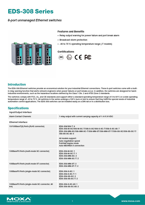
EDS-308Series8-port unmanaged Ethernet switchesFeatures and Benefits•Relay output warning for power failure and port break alarm •Broadcast storm protection•-40to 75°C operating temperature range (-T models)CertificationsIntroductionThe EDS-308Ethernet switches provide an economical solution for your industrial Ethernet connections.These 8-port switches come with a built-in relay warning function that alerts network engineers when power failures or port breaks occur.In addition,the switches are designed for harsh industrial environments,such as the hazardous locations defined by the Class 1Div.2and ATEX Zone 2standards.The switches comply with FCC,UL,and CE standards and support either a standard operating temperature range of 0to 60°C or a wide operating temperature range of -40to 75°C.All switches in the series undergo a 100%burn-in test to ensure that they fulfill the special needs of industrial automation control applications.The EDS-308switches can be installed easily on a DIN rail or in a distribution box.SpecificationsInput/Output InterfaceAlarm Contact Channels1relay output with current carrying capacity of 1A @24VDCEthernet Interface10/100BaseT(X)Ports (RJ45connector)EDS-308/308-T:8EDS-308-M-SC/308-M-SC-T/308-S-SC/308-S-SC-T/308-S-SC-80:7EDS-308-MM-SC/308-MM-SC-T/308-MM-ST/308-MM-ST-T/308-SS-SC/308-SS-SC-T/308-SS-SC-80:6All models support:Auto negotiation speed Full/Half duplex modeAuto MDI/MDI-X connection100BaseFX Ports (multi-mode SC connector)EDS-308-M-SC:1EDS-308-M-SC-T:1EDS-308-MM-SC:2EDS-308-MM-SC-T:2100BaseFX Ports (multi-mode ST connector)EDS-308-MM-ST:2EDS-308-MM-ST-T:2100BaseFX Ports (single-mode SC connector)EDS-308-S-SC:1EDS-308-S-SC-T:1EDS-308-SS-SC:2EDS-308-SS-SC-T:2100BaseFX Ports (single-mode SC connector,80km)EDS-308-S-SC-80:1EDS-308-SS-SC-80:2Standards IEEE802.3for10BaseTIEEE802.3u for100BaseT(X)and100BaseFXIEEE802.3x for flow controlOptical Fiber800Typical Distance4km5km40km80kmWavelen-gthTypical(nm)130013101550TX Range(nm)1260to13601280to13401530to1570 RX Range(nm)1100to16001100to16001100to1600Optical PowerTX Range(dBm)-10to-200to-50to-5 RX Range(dBm)-3to-32-3to-34-3to-34 Link Budget(dB)122929 Dispersion Penalty(dB)311Note:When connecting a single-mode fiber transceiver,we recommend using anattenuator to prevent damage caused by excessive optical power.Note:Compute the“typical distance”of a specific fiber transceiver as follows:Linkbudget(dB)>dispersion penalty(dB)+total link loss(dB).DIP Switch ConfigurationEthernet Interface Port break alarmSwitch PropertiesMAC Table Size2kbitsPacket Buffer Size768KProcessing Type Store and ForwardPower ParametersInput Current EDS-308/308-T:0.07A@24VDCEDS-308-M-SC/S-SC Series,308-S-SC-80:0.12A@24VDCEDS-308-MM-SC/MM-ST/SS-SC Series,308-SS-SC-80:0.15A@24VDC Connection1removable6-contact terminal block(s)Operating Voltage9.6to60VDCInput Voltage Redundant dual inputs,12/24/48VDCReverse Polarity Protection SupportedOverload Current Protection SupportedPhysical CharacteristicsHousing MetalIP Rating IP30Dimensions53.6x135x105mm(2.11x5.31x4.13in)Weight790g(1.75lb)Installation DIN-rail mounting,Wall mounting(with optional kit) Environmental LimitsOperating Temperature Standard Models:-10to60°C(14to140°F)Wide Temp.Models:-40to75°C(-40to167°F) Storage Temperature(package included)-40to85°C(-40to185°F)Ambient Relative Humidity5to95%(non-condensing)Standards and CertificationsHazardous Locations ATEX,Class I Division2EMI CISPR32,FCC Part15B Class AMaritime DNV-GLEMC EN55032/24Vibration IEC60068-2-6EMS IEC61000-4-2ESD:Contact:6kV;Air:8kVIEC61000-4-3RS:80MHz to1MHz:20V/mIEC61000-4-4EFT:Power:2kV;Signal:1kVIEC61000-4-5Surge:Power:2kV;Signal:2kVIEC61000-4-6CS:10VIEC61000-4-8PFMFSafety UL508,UL60950-1,CSA C22.2No.60950-1 Shock IEC60068-2-27Freefall IEC60068-2-32MTBFTime255,528hrsStandards MIL-HDBK-217FWarrantyWarranty Period5yearsDetails See /warrantyPackage ContentsDevice1x EDS-308Series switchInstallation Kit1x cap,plastic,for SC fiber port2x cap,plastic,for SC fiber port(-SC models)2x cap,plastic,for ST fiber port(-ST models) Documentation1x quick installation guide1x warranty cardDimensionsOrdering InformationModel Name 10/100BaseT(X)PortsRJ45Connector100BaseFX PortsMulti-Mode,SCConnector100BaseFX PortsMulti-Mode,STConnector100BaseFX PortsSingle-Mode,SCConnectorOperating Temp.EDS-3088–––0to60°CEDS-308-T8–––-40to75°C EDS-308-M-SC71––0to60°CEDS-308-M-SC-T71––-40to75°C EDS-308-MM-SC62––0to60°CEDS-308-MM-SC-T62––-40to75°C EDS-308-MM-ST6–2–0to60°CEDS-308-MM-ST-T6–2–-40to75°C EDS-308-S-SC7––10to60°CEDS-308-S-SC-T7––1-40to75°C EDS-308-SS-SC6––20to60°CEDS-308-SS-SC-T6––2-40to75°C EDS-308-S-SC-807––10to60°CEDS-308-SS-SC-806––20to60°C Accessories(sold separately)Power SuppliesDR-120-24120W/2.5A DIN-rail24VDC power supply with universal88to132VAC or176to264VAC input byswitch,or248to370VDC input,-10to60°C operating temperatureDR-452445W/2A DIN-rail24VDC power supply with universal85to264VAC or120to370VDC input,-10to50°C operating temperatureDR-75-2475W/3.2A DIN-rail24VDC power supply with universal85to264VAC or120to370VDC input,-10to60°C operating temperatureMDR-40-24DIN-rail24VDC power supply with40W/1.7A,85to264VAC,or120to370VDC input,-20to70°Coperating temperatureMDR-60-24DIN-rail24VDC power supply with60W/2.5A,85to264VAC,or120to370VDC input,-20to70°Coperating temperatureWall-Mounting KitsWK-46Wall-mounting kit,2plates,8screws,46.5x66.8x1mmRack-Mounting KitsRK-4U19-inch rack-mounting kit©Moxa Inc.All rights reserved.Updated Jan30,2019.This document and any portion thereof may not be reproduced or used in any manner whatsoever without the express written permission of Moxa Inc.Product specifications subject to change without notice.Visit our website for the most up-to-date product information.。
Atmel CryptoAuthentication

Application Note Single-Wire and I2C Interfaces Seamless DebuggingUsing Saleae Logic AnalyzerATSHA204A, ATECC108A, and ATECC508A Prerequisites●Hardware PrerequisitesAtmel® AT88CK490 or AT88CK590 Demo-Evaluation Board orAtmel AT88CK101-() KitSaleae Logic Analyzer●Software PrerequisitesAtmel Crypto Evaluation Studio (ACES)IntroductionThe purpose of this document is to help the user gain a better understanding of how to use the Atmel CryptoAuthentication™ ATSHA204A, ATECC108A, and ATECC508A devices (crypto device) with the Saleae Logic Analyzer. The Saleae Logic Analyzer is a powerful tool to debug and evaluate the commands coming to and from these devices. The tool supports both the standard I2C and the Atmel Single-Wire Interface (SWI) protocols.The goal of this application note is to:●Understand the bus interfaces of the crypto device using the Saleae LogicAnalyzer.●Develop and debug with the crypto device using the Saleae Logic Analyzer. SummaryThe Saleae Logic Analyzer provides an in depth tool to quickly develop and debug integration of the crypto device into a customer’s system. The bus decoding allows for easy understanding of all bus traffic to the crypto device. By reducing the development time, the Saleae Logic Analyzer greatly reduces the cost of adding the crypto device.CryptoAuthentication for Single-Wire and I 2C Interfaces Seamless Debugging Using SaleaeLogic Analyzer [APPLICATION NOTE]Atmel-8847B-CryptoAuth-SWI-I2C-Seamless-Debugging-Saleae-Logic-Analyzer-ApplicationNote_08201521.Saleae Logic AnalyzerOn load of the analyzer, either 8 or 16 channels will display depending on the analyzer used. Protocol specific settings are located on the far right under the heading, Analyzers .Figure 1-1.Channels and Protocol SettingsThe crypto device supports either a Single-Wire Interface (SWI) or I 2C Interface depending on the P/N. ●SWI — Supported through the use of a DLL library. Use version 1.1.16 or greater. This version comes with support on Win, LNX, and IOS.●I 2C — Supported by the use of the built-in I 2C interface that is included in the Saleae download.3CryptoAuthentication for Single-Wire and I 2C Interfaces Seamless Debugging Using SaleaeLogic Analyzer [APPLICATION NOTE]Atmel-8847B-CryptoAuth-SWI-I2C-Seamless-Debugging-Saleae-Logic-Analyzer-ApplicationNote_0820152.Single-Wire Interface (SWI)Use the SWI DLL library version 1.1.16 or greater.1.Copy the DLL into the Saleae LLC\Analyzers directory on the user’s PC. Once the driver has been copied to the correct folder, the Atmel SWI option will appear and be listed in the Analyzer drop-down options. The SWI Analyzer has three display modes:Token Byte Packet (as described in the datasheet)Figure 2-1.Atmel SWI Option2.Select the Atmel SWI Analyzer from the list. 3.After selecting Atmel SWI Analyzer , rename the channel when prompted, 4.Select the Falling Edge Trigger option and start sampling. Using ACES, select a command and send it to the device. For an overview of the ACES tool, please see “Using ACES Application Note”. This will cause the bus to become active and the Analyzer will trigger on the first falling edge and data line.In the screen shot below, the Wake command has been captured followed by Wake Status Read. The Wake command is a special token designed to wake the device and reset the watchdog timer.Figure 2-2.Wake Command Followed by Wake Status ReadEnlargement ofthe Analyzerpull-down options.CryptoAuthentication for Single-Wire and I 2C Interfaces Seamless Debugging Using SaleaeLogic Analyzer [APPLICATION NOTE]Atmel-8847B-CryptoAuth-SWI-I2C-Seamless-Debugging-Saleae-Logic-Analyzer-ApplicationNote_0820154The token view displays each logic bit which is made up of seven bits on the wire. Each group of seven bits is encoded either as a Logic 1 or Logic 0 as follows:●A Logic 1 is one low bit followed by six high bits. ● A Logic 0 is one low bit followed by one high bit, then by one low bit, and then by four high bits.Figure 2-3.Token View Figure 2-4.Logic BitsThe byte view builds on the token view by combining eight tokens into a single byte. This view allows for easy matching of information on the data bus to the command set defined in the datasheet. The byte view istransmitted with the less significant bit first.Figure 2-5.BytesThe packet view further builds on the byte view by ordering the data into logic packets based on the datasheet definition. This allow for quick and easy review of the commands without the need to reference the datasheet.Figure 2-6.Packets0x880x045CryptoAuthentication for Single-Wire and I 2C Interfaces Seamless Debugging Using SaleaeLogic Analyzer [APPLICATION NOTE]Atmel-8847B-CryptoAuth-SWI-I2C-Seamless-Debugging-Saleae-Logic-Analyzer-ApplicationNote_0820153.I 2C InterfaceThe crypto device supports an I 2C interface that is directly supported by the Saleae tool.1.To configure the Analyzer for I 2C , select the I2C option from the Analyzer drop-down list and follow the configuration guide.Figure 3-1.I2C Analyzer Option 2.Select the clock and data channels that will be used for the I2C bus. Different encoding options can also be selected. The crypto device uses the default 8-bit encoding.Figure 3-2.Clock and Data Channels Enlargement ofthe Analyzerpull-down options.CryptoAuthentication for Single-Wire and I 2C Interfaces Seamless Debugging Using SaleaeLogic Analyzer [APPLICATION NOTE]Atmel-8847B-CryptoAuth-SWI-I2C-Seamless-Debugging-Saleae-Logic-Analyzer-ApplicationNote_0820156 3.Next, the Update Channel Names dialog box will be prompted to rename the channels to reflect SCL andSDA. This is an optional step, but helps when analyzing more then one bus at a time.Figure 3-3.Update Channel Names 4.Now that the analyzer is configured, set-up the trigger settings. The Saleae has a One Shot trigger thatcan be triggered on either the falling or rising edge of the SCL channel. The bus is normally held high;therefore, setting a falling edge trigger is recommended.Figure 3-4.Trigger Settings7CryptoAuthentication for Single-Wire and I 2C Interfaces Seamless Debugging Using SaleaeLogic Analyzer [APPLICATION NOTE]Atmel-8847B-CryptoAuth-SWI-I2C-Seamless-Debugging-Saleae-Logic-Analyzer-ApplicationNote_0820155.Once the analyzer has been started, execute a command in order to generate data on the bus.Figure 3-5.Execute a Command After the Analyzer has been triggered, it will collect the waveform information and display it in the viewer. The first token shown is the ATSHA204 Wake.Figure 3-6.First Token — ATSHA204 WakeThe Wake command is a special command that is required to wake-up the device. The command consists of a I 2C Start event followed by a long period of Logic 0 on the SDA line, then followed a Stop event.Figure 3-7.Wake CommandCryptoAuthentication for Single-Wire and I 2C Interfaces Seamless Debugging Using SaleaeLogic Analyzer [APPLICATION NOTE]Atmel-8847B-CryptoAuth-SWI-I2C-Seamless-Debugging-Saleae-Logic-Analyzer-ApplicationNote_0820158After a Wake command, an optional Read can be performed to read the status of the crypto device as shown in the waveform below. After the Read command is issued, the device will send four bytes of data (1-count, 1-data, and 2-CRC).Figure 3-8.Read WaveformThe Saleae tool supports a variety of display options for the I 2C interface including Binary, Hex, and ASCII to help quickly and easily evaluate the data. It can be selected by clicking the Configuration button next to the analyzer of interest on the right.Figure 3-9.Display Options4.Revision HistoryX X X X X XAtmel Corporation 1600 Technology Drive, San Jose, CA 95110 USA T: (+1)(408) 441.0311F: (+1)(408) 436.4200| © 2015 Atmel Corporation. / Rev.: Atmel-8847B-CryptoAuth-SWI-I2C-Seamless-Debugging-Saleae-Logic-Analyzer-ApplicationNote_082015.Atmel ®, Atmel logo and combinations thereof, Enabling Unlimited Possibilities ®, CryptoAuthentication ™, and others are registered trademarks or trademarks of Atmel Corporation in U.S. and other countries. Other terms and product names may be trademarks of others.DISCLAIMER: The information in this document is provided in connection with Atmel products. No license, express or implied, by estoppel or otherwise, to any intellectual property right is granted by this document or in connection with the sale of Atmel products. EXCEPT AS SET FORTH IN THE ATMEL TERMS AND CONDITIONS OF SALES LOCATED ON THE ATMEL WEBSITE, ATMEL ASSUMES NO LIABILITY WHATSOEVER AND DISCLAIMS ANY EXPRESS, IMPLIED OR STATUTORY WARRANTY RELATING TO ITS PRODUCTS INCLUDING, BUT NOT LIMITED TO, THE IMPLIED WARRANTY OF MERCHANTABILITY, FITNESS FOR A PARTICULAR PURPOSE, OR NON-INFRINGEMENT. IN NO EVENT SHALL ATMEL BE LIABLE FOR ANY DIRECT, INDIRECT, CONSEQUENTIAL, PUNITIVE, SPECIAL OR INCIDENTAL DAMAGES (INCLUDING, WITHOUT LIMITATION, DAMAGES FOR LOSS AND PROFITS, BUSINESS INTERRUPTION, OR LOSS OF INFORMATION) ARISING OUT OF THE USE OR INABILITY TO USE THIS DOCUMENT, EVEN IF ATMEL HAS BEEN ADVISED OF THE POSSIBILITY OF SUCH DAMAGES. Atmel makes no representations or warranties with respect to the accuracy or completeness of the contents of this document and reserves the right to make changes to specifications and products descriptions at any time without notice. Atmel does not make any commitment to update the information contained herein. Unless specifically provided otherwise, Atmel products are not suitable for, and shall not be used in, automotive applications. Atmel products are not intended,authorized, or warranted for use as components in applications intended to support or sustain life.SAFETY-CRITICAL, MILITARY, AND AUTOMOTIVE APPLICATIONS DISCLAIMER: Atmel products are not designed for and will not be used in connection with any applications where the failure of such products would reasonably be expected to result in significant personal injury or death (“Safety-Critical Applications”) without an Atmel officer's specific written consent. Safety-Critical Applications include, without limitation, life support devices and systems, equipment or systems for the operation of nuclear facilities and weapons systems.Atmel products are not designed nor intended for use in military or aerospace applications or environments unless specifically designated by Atmel as military-grade. Atmel products are not designed nor intended for use in automotive applications unless specifically designated by Atmel as automotive-grade.。
SE8025TC说明书V2
SE8025TC 使用说明
SE8025TC 使用说明概要
1 2 3 SE8025TC 的特点: ................................................................................................................ 2 SE8025TC 结构框图: ........................................................................................................... 2 SE8025TC 管脚定义: ........................................................................................................... 3 3.1 管脚封装:........................................................................................................................ 3 3.1 管脚功能定义:................................................................................................................ 3 绝对电气指标:..............................................................................................................
802说明书

YCE C6mini快速入门指南安装使用产品前请先阅读本指南,并请保留备用欢迎使用YCE手机!感谢您选择本公司数字移动电话。
POMP C6mini是由强大团队倾情打造,为您提供高品质的移动通信和娱乐体验。
●您可以通过阅读本手册,全面地了解本智能手机的使用,领略其完善的功能和简洁的操作方法。
使用手机前,请仔细阅读全部安全注意事项和本用户手册,以确保安全和正确使用。
●本用户手册中所用的插图仅作为示意用图,可能与手机有所不同,请以你的手机为准。
●本手册中描述的某些服务和功能取决于网络和预定服务。
●收发信息、上传和下载、进行同步和使用定位服务等可能会产生其他费用。
如欲避免产生额外费用,请选择合适的实际收费计划。
有关详细信息,请联系服务运营商。
安全警告和注意事项将手机放在儿童和宠物等接触不到的地方。
以防可能吞下小零件导致窒息或发生危险。
安全开机,当禁止使用手机或手机的使用会引起干扰或危险时,请不要开机。
请遵守当地的所有相关法律法规。
请使用双手驾驶汽车。
开车时使用手机应首先考虑交通安全。
所有的无线设备都可能受到干扰,从而影响性能。
在医疗或卫生保健机构可能会使用对无线频率敏感的设备。
在飞机上应关机。
请遵守任何的相关的限制规定。
无线设备会对飞机产生干扰。
在加油站或靠近燃料、化学制剂的地方,请不要使用手机。
注意:●您的手机只能使用本公司指定的电池和充电器。
使用其它的产品可能会造成电池漏液、过热、爆裂和起火。
●请使用220V交流电。
使用其它电压会引起漏电、起火和对手机及充电器的损坏。
●禁止短路充电器,否则会引起触电、冒烟和对充电器的损坏。
●请不要在电源线损坏的情况下使用充电器,否则会导致起火和触电。
●请不要拆卸或改装充电器,否则会导致人身伤害、触电、起火和充电器损坏。
●拔插头时要抓住充电器,拉电源线会损坏电线,引起触电和起火。
●手机、电池和充电器无防水性能,请勿在浴室等高湿度的地方使用,同样也要避免被雨淋湿。
●用柔软的干布清洁手机、电池和充电器。
NCR RealPOS 80硬件用户手册说明书

NCR RealPOS 80 hardware user ManualNCR RealPOS 80Release 1.0Hardware User's GuideB005-0000-1440Issue Av Table of ContentsChapter 1: Product OverviewIntroduction...........................................................................................1-1 Cabinet.............................................................................................1-2Configurations................................................................................1-4Integrated Terminal...................................................................1-4Integrated Terminal w/Cash Drawer.....................................1-5Left/Right Configurability.......................................................1-6 Serial Number/Model Number Label...............................................1-7Features..................................................................................................1-8 Processor Board..............................................................................1-84-Port USB Daughter Card............................................................1-9ATX Riser Card...............................................................................1-9Front Control Panel......................................................................1-10Storage Media...............................................................................1-10Power Supply................................................................................1-11Operating Systems.......................................................................1-11UPS.................................................................................................1-11 Power Management............................................................................1-12 Definitions of the states involved...............................................1-13 Operator Displays...............................................................................1-17 5964 12.1-Inch Touch Screen.......................................................1-17Features.....................................................................................1-175942 12.1-INCH Color LCD.........................................................1-197452-K309/K404 9-Inch Monochrome CRT..............................1-207452-K419 15-Inch Color CRT.....................................................1-20NCR 5982 5-Inch LCD Display...................................................1-21 NCR 5953 12.1-Inch DynaKey...........................................................1-22viNCR 5952 10.4-Inch DynaKey...........................................................1-23NCR 5932 Keyboards.........................................................................1-24109-Key USB Keyboard...............................................................1-24Features.....................................................................................1-25115-Key PS/2 Big Ticket Keyboard............................................1-2668-Key PS/2 POS Keyboard........................................................1-27Features.....................................................................................1-27NCR 5972 2x20 Remote Customer Display.....................................1-31Features..........................................................................................1-31NCR 5973 2x20 International VFD Customer Display..................1-32Features..........................................................................................1-32Printers.................................................................................................1-33NCR 7158 Printer..........................................................................1-33NCR 7162 Printer..........................................................................1-34NCR 7194 Printer..........................................................................1-34NCR 7167 Printer..........................................................................1-35NCR 7197 Printer..........................................................................1-35System Configuration Diagrams......................................................1-36Chapter 2: Hardware InstallationIntroduction...........................................................................................2-1Installation Restrictions.................................................................2-1Installing the Integration Tray............................................................2-2Installing the Keyboard........................................................................2-3PS/2 Keyboard/Mouse Cable Connections...............................2-5Dual Port Keyboard/Mouse Installation................................2-5Mouse Installation Restriction..................................................2-5Installing the Integrated Operator Display.......................................2-6Operator Display Cable Connections........................................2-10Installing an NCR 5964 12.1-inch Touch LCD.....................2-10Installing a 5942 12.1-Inch LCD Monitor..............................2-13viiInstalling the Integrated Customer Display....................................2-14 Installing the Transaction Printer.....................................................2-16 Printer Cable Connections...........................................................2-18USB Installation........................................................................2-18RS-232 Installation w/Power from Powered USB..............2-19 Installing an NCR 5972 Remote Customer Display.......................2-20 Customer Display Cable Connections.......................................2-21 Installing an NCR 5973 Remote Customer Display.......................2-22 Customer Display Cable Connections.......................................2-23 Installing a 5953 DynaKey.................................................................2-24 Installing a 5952 DynaKey.................................................................2-25 Installing a Secondary CRT Display (Dual Display)......................2-26 Installing the Hardware...............................................................2-26Supported Configurations......................................................2-26Supported Configurations by Operating System................2-27Supported Hardware Configurations...................................2-27Installing the Displays.............................................................2-28Configuring the Software for Dual Display..............................2-29 Installing an NCR 5982 5-Inch Operator Display...........................2-30 Installing the PCI LCD Board (5952-K052)................................2-31Connecting the 5982 Display to the Terminal......................2-32 Installing a Cash Drawer...................................................................2-33 Installing a Second Cash Drawer...........................................2-33Chapter 3: SetupIntroduction...........................................................................................3-1 Entering Setup Using a Keyboard......................................................3-1 How to Select Menu Options..............................................................3-1 Restoring Factory Settings...................................................................3-2 Special DynaKey Keypad Mode.........................................................3-2 Normal DynaKey Keypad Operating Mode..............................3-4viiiDisabling Resources..............................................................................3-5BIOS Default Values.............................................................................3-5Main Menu......................................................................................3-5Advanced Menu.............................................................................3-8Security Menu...............................................................................3-12Power Menu..................................................................................3-12Boot Sequence...............................................................................3-12Chapter 4: Operating System RecoveryIntroduction...........................................................................................4-1Prerequisites....................................................................................4-1Connecting an External Backpack CD-ROM Drive...................4-2Updating Procedures.....................................................................4-3Completing the OS Installation (Windows 2000)..................4-5Completing the OS Installation (Windows NT 4.0)..............4-5Completing the OS Installation (Windows EXe)...................4-6Completing the OS Installation (DOS)....................................4-6Gold Disk Contents...............................................................................4-7NCR 7456/58 Windows 2000 Operating System RecoverySoftware (LPIN: D370-0536-0100).................................................4-7Installed Software:.....................................................................4-7Software Drivers.........................................................................4-8Special Settings...........................................................................4-8Recommendation.......................................................................4-9NCR 7456/58 Windows NT 4.0 Operating SystemRecovery Software (LPIN: D370-0564-0100)............................4-10Installed Software:...................................................................4-10Software Drivers.......................................................................4-10Special Settings.........................................................................4-11Recommendation.....................................................................4-12ix NCR RealPOS 80/80c Windows XPe Operating SystemRecovery Software (LPIN: D370-0570-0100).............................4-13Installed Software:...................................................................4-13Software Drivers.......................................................................4-13Special Settings.........................................................................4-14Recommendation.....................................................................4-14 OS Recovery from a Larger Disk Image..........................................4-15Chapter 5: BIOS Updating ProceduresIntroduction...........................................................................................5-1 Prerequisites....................................................................................5-1Connecting an External Backpack CD-ROM Drive...................5-2Updating Procedures.....................................................................5-3 BIOS Crisis Recovery............................................................................5-5 Recovery Procedures......................................................................5-6 Cable/Connector Pin-Out Information.............................................5-9Chapter 6: Memory DumpGeneral Memory Dump Information.................................................5-1 BIOS Requirements........................................................................5-1Disk Format.....................................................................................5-1Supported Operating Systems......................................................5-2Summary of Operating Systems..............................................5-3Prerequisites....................................................................................5-3Windows XP/2000.....................................................................5-4Windows NT...............................................................................5-5 DOS Memory Dump Specifics............................................................5-6 Dump Process Overview...............................................................5-6Restrictions and Limitations.........................................................5-6Performing the Memory Dump....................................................5-9Configuring the Terminal.........................................................5-9xDump Procedure........................................................................5-9Tunes/Tones.............................................................................5-10Moving the Files to Hard Disk and Reassembling..............5-12Flow Chart.................................................................................5-13Memory Dump Assembler..........................................................5-14Appendix A: Retail Keyboard Key Layouts68-Key Keyboard..................................................................................A-1DynaKey.........................................................................................A-4Special DynaKey Keypad Mode.............................................A-4Normal DynaKey Keypad Operating Mode.........................A-65932 USB Keyboard.......................................................................A-7 Appendix B: Feature KitsAppendix C: CablesPrinter Cables.......................................................................................C-1Scanner Cables......................................................................................C-37872 or 7875 Scanner/Scale (RS-232)..........................................C-37872 or 7875 Scanner/Scale (Powered USB)..............................C-37892 Scanner (Powered RS-232)..................................................C-37882 Scanner (Powered RS-232)..................................................C-47837 Scanner (Powered RS-232)..................................................C-4Display Cables......................................................................................C-5VGA Display, Mono......................................................................C-5VGA Display, Color......................................................................C-5CRT AC Power Extension............................................................C-55982 5-Inch LCD............................................................................C-65953 DynaKey................................................................................C-65953 DynaKey w/Insert...............................................................C-6Wedge Keyboard Y-Cable............................................................C-7xi5972 VFD Customer Display (Powered RS-232).......................C-7DVI to DVI for 5964.......................................................................C-7PS/2 - RS-232 & Power for 5964..................................................C-8Wedge Keyboard Adapter...........................................................C-812.1-Inch LCD Aux Power Cable................................................C-8Cash Drawer Cables............................................................................C-9 Dual Cash Drawer, Y-Cable.........................................................C-9Cash Drawer, Extension Cable....................................................C-9 Ethernet Communications Cable.......................................................C-9 Keyboard Cables................................................................................C-10 PS/2 Keyboard Extension..........................................................C-10PS/2 Y-Cable................................................................................C-10 Signature Capture/Electronic Payment Terminal Cable.............C-11 5945/5992 EPT (RS-232 w/Power)...........................................C-115942 12V Power Cable.................................................................C-11 IDE Cables...........................................................................................C-12 IDE Interface Cable (3-Connector)............................................C-12IDE Interface Cable (2-Connector)............................................C-12 Compact Flash Power Cable.............................................................C-12 Power Cables......................................................................................C-13 AC Power......................................................................................C-13Appendix D: Memory MapDOS Considerations............................................................................D-2 Non-TAPS DOS Environment.....................................................D-3TAPS DOS Environment..............................................................D-3This is a “Table of Contents preview” for quality assuranceThe full manual can be found at /estore/catalog/ We also offer free downloads, a free keyboard layout designer, cable diagrams, free help andsupport. : the biggest supplier of cash register and scale manuals on the net。
MA801_MA802_A9
6. 存储器组织................................................................................................... 19
7. 数据指针寄存器(DPTR)................................................................................ 23 8. 系统时钟 ...................................................................................................... 24
2012/11 version A9
2
MA801_MA802 1 中央处理器 MA801_MA802 8K 字节 Flash ROM ━ ISP 存储空间可以选择 1.0KB, 2.0KB 或 3.0KB ━ 用于 Flash 存储器访问的两级代码保护 ━ Flash 写/擦除周期: 20,000 ━ Flash 数据保留时间: 在 25℃下 100 年 片上 256 字节暂存 RAM 中断控制器 ━ 7 个中断源,4 级优先级 ━ 两个外部中断输入,INT0 和 INT1 两个 16 位定时/计数器, Timer 0 和 Timer 1. ━ Timer 0/1 可以选择 X12 模式 可编程的 16 位计数/定时阵列(PCA) 支持 2 通道 PWM ━ 捕获模式 ━ 16 位软件定时器模式 ━ 高速输出模式 ━ 8 位 PWM 模式 增强型 UART (S0) ━ 帧错误检测 ━ 自动地址识别 8 位 ADC ━ 可编程吞吐率达到 100 ksps ━ 8 通道单端输入 主/从 SPI 串行接口 可编程看门狗定时器,由 CPU 或上电一次使能。 在 20 脚封装下最多 15 个 GPIO。 ━ 可以配置成双向口,推挽输出,漏极开路和仅输入 多种电源控制模式:空闲模式和掉电模式 ━ 所有中断可以唤醒空闲模式 ━ 2 个源可以唤醒掉电模式 低压侦测器:对于 MA801 是 VDD 3.7V ,对于 MA802 是 VDD 2.4V 工作电压范围 Operating voltage range: ━ MA801: 4.5V~5.5V, 要求 Flash 写操作最小是 4.5V (ISP/IAP) ━ MA802: 2.4V~3.6V, 要求 Flash 写操作最小是 2.7V (ISP/IAP) 工作频率范围: 25MHz(最大) ━ MA801: 0 – 25MHz @ 4.5V – 5.5V ━ MA802: 0 – 12MHz @ 2.4V – 3.6V and 0 – 25MHz @ 2.7V – 3.6V 时钟源 ━ 外部晶振模式和内置 RC 振荡器 (IRCO, 6MHz) 工作温度: ━ 工业级 (-40℃ to +85℃)* 封装类型: ━ PDIP20: MA801AE/MA802AE ━ SOP20: MA801AS/MA802AS ━ TSSOP20: MA801AT/MA802AT
SC802_08资料
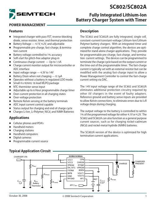
POWER MANAGEMENT Fully Integrated Lithium-Ion Battery Charger System with TimerFeaturesIntegrated charger with pass FET, reverse-blocking diode, sense resistor, timer, and thermal protection Battery Voltage — 4.1V, 4.2V, and adjustableProgrammable pre-charge, fast-charge, & termina-tion currentBattery voltage controlled to 1% accuracy Soft-start for glitch-free adaptor plug-in Continuous charge current — Up to 1.5ACharge current monitor output for microcontroller or ADC interfaceInput voltage range — 4.3V to 14VBattery Drain when not charging — 0.1μAOperates without a battery in regulated LDO mode Small 4 x 4(mm) 16 lead MLPQ package NTC thermistor sense inputAdjustable up to 6 Hour programmable charge timer Over-current protection in all charging states Over-voltage protectionRemote Kelvin sensing at the battery terminals ADC input current control capableStatus output for charging and end of charge cycle Charges Li-Ion, Li-Polymer, NiCd, and NiMH BatteriesApplicationsCellular phones and PDA’s Handheld meters Charging stations Handheld computers Digital camerasProgrammable current sourceDescriptionThe SC802 and SC802A are fully integrated, single cell, constant-current/constant-voltage Lithium-Ion/Lithium Polymer battery chargers. With an integrated timer and complete charge control algorithm, the devices are opti-mized for stand-alone charger applications. They provide for programmable pre-charge, fast-charge, and termina-tion current settings. The devices can be programmed to terminate the charge cycle based on the output current or the time-out of the programmable timer. The fast-charge current is typically set with an external resistor but can be modified with the analog fast-charge input to allow a Power Management Controller to control the fast-charge current setting via DAC.The 14V input voltage range of the SC802 and SC802A eliminates additional protection circuitry required by other 5V chargers in the event of faulty adapters. Reference ground and battery sense inputs are provided to allow Kelvin connections, to eliminate errors due to I×R voltage drops during charging.The output voltage to the battery is controlled to within 1% of the programmed voltage for either 4.1V or 4.2V. The SC802 and SC802A can also function as a general purpose current sources, such as for charging nickel-cadmium (NiCd) and nickel-metal-hydride (NiMH) batteries.The SC802A version of the device is optimized for high termination current applications.Typical Application CircuitPin Confi gurationMarking InformationOrdering InformationDevicePackageSC802IMLTRT (1)(2)MLP16 SC802AIMLTRT (1)(2)MLP16 SC802EVB (3)Evaluation Board SC802AEVB (3)Evaluation BoardNotes:(1) Available in tape and reel only. A reel contains 3,000 devices.(2) Available in lead-free package only. Device is WEEE and RoHScompliant.(3) Specify the part number when ordering.802yywwyyww = datecode802A yywwyyww = datecodeExceeding the above specifi cations may result in permanent damage to the device or device malfunction. Operation outside of the parametersspecifi ed in the Electrical Characteristics section is not recommended.NOTES:(1) VCC1 and VCC2, and VOUT1 and VOUT2, must be connected, and will be referred to collectively as VCC and VOUT, respectively. All referencesto V VCC , V VOUT , I VCC , and I VOUT refer to the common node voltage and total current of VCC1 and VCC2, and VOUT1 and VOUT2, respectively.(2) Tested according to JEDEC standard JESD22-A114-B.(3) Operating voltage is the input voltage at which the charger is guaranteed to begin operation. Maximum operating voltage is the maximumVsupply as defi ned in EIA/JEDEC Standard Number 78, paragraph 2.11.(4) Calculated from package in still air, mounted to 3 x 4.5(in), 4 layer FR4 PCB with thermal vias under the exposed pad per JESD51 standards.Absolute Maximum RatingsVCC1, VCC2, EN_NTC (V) . . . . . . . . . . . . . . . . . . . -0.3 to +14.0VOUT1, VOUT2, RTIME(V) . . . . . . . . . . . . . . . . . -0.3 to +6.0BIPB, CPB, CHRGB (V) . . . . . . . . . . . . . . . . . . . . . -0.3 to +6.0 IPRGM, ITERM, AFC (V) . . . . . . . . . . . . . . . . . . . . -0.3 to +6.0 VPRGM, BSEN (V) . . . . . . . . . . . . . . . . . . . . . . . . . -0.3 to +6.0REFGND to GND (V) . . . . . . . . . . . . . . . . . . . . . . . -0.3 to +0.3VOUT Short to GND (1) . . . . . . . . . . . . . . . . . . . . . . Continuous ESD Protection Level (2)(kV) . . . . . . . . . . . . . . . . . . . . . . . . . . . . 2Recommended Operating ConditionsAmbient Temperature Range (°C) . . . . . . . . -40 < T A < +85VCC Operating Voltage (1)(3) (V) . . . . . . . . 4.3 < V VCC1,2 < 6.5Thermal InformationThermal Resistance, Junction to Ambient (4) (°C/W) . . . . 50Maximum Junction Temperature (°C) . . . . . . . . . . . . . . +150Storage Temperature Range (°C) . . . . . . . . . . . . -65 to +150Peak IR Refl ow Temperature (10s to 40s) (°C) . . . . . . . +260Test Conditions: V VCC = 5.00V (1), V VOUT = 3.70V unless specifi ed. Typ values at 25°C. Min and Max at -40°C < T A < 85°C, unless specifi ed.ParameterSymbolConditions MinTypMaxUnitsVCC UVLO Rising Threshold VT UVLOR 3.74.0 4.3V VCC UVLO Hysteresis VT UVLOH 40mVVCC OVP Rising Threshold VT OVPR 6.5 6.87.5V VCC OVP Falling Threshold VT OVPF 6.16.57.1V VCC OVP HysteresisVT OVPH VT OVPR - VT OVPF200300500mVOperating CurrentICC DISV EN_NTC = 0V, CHRGB, CPB off 2.6mAICC CHG V EN_NTC = 0.5 × V VCC , CHRGB, CPB off 1 2.4 3.5ICC LDOLDO Mode, CHRGB, CPB off 81623Battery Leakage Current (sum of I VOUT and I BSEN )ILeak BAT V VCC = 0V, V VOUT = V BSEN = 4.5V0.12μA Regulated VoltageV CV-HI V VPRGM = V VCC 4.16 4.20 4.24VV CV_LOV VPRGM = 0V4.06 4.10 4.14REFGND Output Accuracy V VOUT_RGND V VOUT_RGND = V VOUT - V CV n , V REFGND = 30mV223038mV REFGND CurrentI REFGNDV REFGND = 0V35μA Electrical CharacteristicsParameterSymbolConditionsMin TypMax UnitsAdjust Mode Feedback Voltage V ADJMF VPRGM = External Divider, 4.2V ≤ VCC ≤ 6.5V3.0VAdjust Mode VPRGM Shunt Resis-tanceR VPGMSHAdjust Mode, V VPRGM = 0.1V0.515kΩAdjust Mode Threshold Voltage VT ADJM V VOUT - V BSEN 50250420mV SC802 Pre-Charge Current I PREQ R ITERM = 3.01kΩ748290mA SC802 Termination Current I TERMQ R ITERM = 3.01kΩ35.54249.5mA SC802 Fast-Charge Current I FastQ R IPRGM = 3.01kΩ, V VOUT = 3.8V 450500550mA SC802 AFC Fast-Charge Current I FQ_ADJ R IPRGM = 3.01kΩ, V AFC = 0.75V200240280mA SC802A Pre-Charge Current I PREQA R ITERM = 976Ω135145160mA SC802A Termination Current I TERMQA R ITERM = 976Ω135145160mA SC802A Fast-Charge Current I FastQA R IPRGM = 1.78kΩ, R ITERM = 976Ω, V VOUT = 3.8V740800860mA SC802A AFC Fast-Charge Current I FQ_ADJA R IPRGM = 1.78kΩ, R ITERM = 976Ω, V AFC = 0.75V, V VOUT = 3.8V310367430mA I PROG Regulated Voltage V IPRGM 1.44.5 1.6V V VOUT Pre-charge Threshold (2)VT PreQ measured at VOUT pins 2.7 2.8 2.9V V VOUT Re-charge Threshold (3)VT ReQ V CV (at BSEN) - V BSEN-FDBK70100140mV Over Temperature ShutdownT OT-R Hysteresis = 10°C 150°CEN_NTC ThresholdsVT NTC_DISDisable (Falling)0.5<1 1.1V RT NTC_HFNTC Hot (Falling), tested at V VCC = 5V 283032%RT NTC_CR NTC Cold (Rising), tested at V VCC = 5V 727578%RT NTC_EN Charger Enable, tested at V VCC = 5V 849092%VT NTC_HYSHot/Cold threshold hysteresis, tested at V VCC = 5V50mVTimer Disable Threshold VT TIMER V RTIME < VT TIMER Disables Timer 0.71 1.1V Internal Timer Select VT INTTS VCC-V RTIME < VT INTTS selects internal timer 1.5VExternal RTIME VoltageV RTIME RTIME tied through 36.5kΩ to GND 1.4 1.5 1.6VPre-Charge Fault Time-out T PreQFRTIME tied through 36.5kΩ to GND50minRTIME tied to VCC-35%45+35Charge Complete Time-outT QCOMPRTIME tied through 36.5kΩ to GND3.3hrRTIME tied to VCC-35%3+35Electrical Characteristics (continued)ParameterSymbolConditionsMin TypMaxUnitsCHRGB Charge LED On V CHRGB Load = 5mA 0.51V CHRGB Charge LED OFF I CHRGB Leakage Current, V = 5V1μA CPB LED On V CPB Load = 5mA 0.51V CPB LED OffI CPB Leakage Current, V = 5V1μABIPB, VPRGM InputsV IH 1.8VV IL0.4Electrical Characteristics (continued)Notes:(1) Electrical Characteristics apply for V VIN = 4.75V to 5.25V, but are tested only at V VIN = 5.00V, unless noted.(2) Pre-charge threshold is applied directly at VOUT for any setting of V CV , whether 4.1V or 4.2V fi xed, or Adjust Mode.(3) Re-charge threshold is relative to V CV as measured at BSEN. For either of the fi xed output voltage settings, V BSEN is compared directly tothe programmed CV regulation voltage. In Adjust Mode, V BSEN is compared to the Adjust Mode feedback voltage, V ADJMF . So the re-charge threshold at the battery is VT ReQ × V CV / V BSEN-FDBK .Typical CharacteristicsOutput Current (SC802) versus R IPRGM00.511.520.751 1.52 2.533.544.555.56.57R IPRGM (k ) C u r r e n t (A )I FQ501001502002500.81.52.53.54.568.51011.8514R ITERM (k )C u r r e n t (m A )I PQI TERM024681020406080T i m e -o u t (h r s )T PreQT QCOMPR RTIME(k ) 0100200300400500600700100080060050045030025020010054Output Current (mA)D r o p o u t V o l t a g e (m V )33.23.43.63.844.24.40255075100125150175200225t (minutes)V O L T A G E (V )0.10.20.30.40.50.6C U R R E N T (A )V VOUTI VOUTV CHRGBOutput Current (SC802) versus R ITERMDrop-out Voltage versus Output CurrentTime-out versus Output R RTIMEBattery Charge Profi leΩΩΩPin DescriptionsPin #Pin Name Pin Function1BSEN Battery voltage sense pin — Connect to battery terminal to Kelvin sense battery voltage, to a resistor divider network for adjustable output voltage, or to VOUT otherwise. Do not leave this pin fl oating.2VPRGM Selectable voltage program pin — Logic low = 4.1V; Logic high = 4.2V; Resistor = adjustable.3IPRGM Charger current program pin in fast-charge mode — Requires a resistor to ground to program fast-charge current.4ITERM Selection for current termination and pre-charge current — Requires a resistor to ground to pro-gram pre-charge and termination current.5REFGND Reference ground — Allows Kelvin connection to battery negative terminal. 6GND Ground7EN_NTC Combined device enable/disable and NTC input pin — Logic high enables device; logic low dis-ables device. Analog voltages between 0.3×VVCCand 0.75×VVCCenable the NTC function.8BIPB Battery In Place Bar (BIPB) — selects Charge/LDO mode. BIPB = Low selects charge mode. BIPB = High selects LDO mode which disables Pre-Charge and timer functions9AFC Analog fast-charge setting — Connect to DAC for analog control of fast-charge current value. Connect to VCC to disable AFC. Do not leave open.10CHRGB Open drain charger status pin — The output is active low when the charger is on and IVOUT> ITERM. The CHRGB output switches to high impedance when IVOUT< ITERM. This pin can sink 10mA.11CPB Open Drain Charger present indicator — The output is active low when the VVCCexceeds VTUVLOR. This pin can sink 10mA.12RTIME Programmable timer input pin — Connect to VCC to select the internal time-out of 3hrs. Connect an external resistor to ground to program the timeout period. Connect to ground to disable the timer.13VCC1Supply pin — Connect to adaptor power and to VCC2. (1) 14VCC2Supply pin — Connect to adaptor power and to VCC1. (1) 15VOUT1Charger output — Connect to battery and to VOUT2. (2) 16VOUT2Charger output — Connect to battery and to VOUT1. (2)T ThermalPad Pad is for heatsinking purposes — The thermal pad is not connected internally. Connect exposed pad to ground plane using multiple vias.Notes:(1) VCC1 and VCC2 must be connected. VCC1 and VCC2 will be referred to collectively as VCC. All references to VVCC and IVCCrefer to the commonnode voltage and total current of VCC1 and VCC2.(2) VOUT1 and VOUT2 must be connected. VOUT1 and VOUT2 will be referred to collectively as VOUT. All references to VVOUT and IVOUTrefer to thecommon node voltage and total current of VOUT1 and VOUT2.Block DiagramVCCBIPBBSENAFCEN-NTCRTIM CPB CHRGB REFGNDVPRGM GNDGeneral OperationThe SC802 and SC802A can be confi gured independently with respect to fast-charge and termination current, output voltage, timing, and operation with and without a battery (LDO mode). A typical charging cycle is described in this section. Details on alternate applications and output programmability are covered in subsequent sec-tions. Wherever the SC802 and SC802A descriptions are the same, the part will be referred to as the SC802/A.The charging cycle begins when the adapter is plugged in. The SC802/A performs glitch fi ltering on the VCC input and initiates a charge cycle when V VCC > VT UVLOR . The CPB and CHRGB signals turn on the charger LED’s. If the battery voltage is less than 2.8V, the SC802/A will charge the output with the pre-charge current. When the battery voltage exceeds 2.8V, the SC802/A enters fast-charge or Constant Current (CC) regulation. When the battery voltage reaches its fi nal value, the charger enters Constant Voltage (CV) regulation. The CV regulation output voltage, (V CV ), can be programmed to fixed values V CV-HI = 4.2V, V CV-LO = 4.1V, or programmed to any voltage V CV-ADJ using the available Adjust Mode. In CV regulation the battery accepts decreasing current until the output current (I VOUT ) reaches the programmed termination current, designated (I TERM ).When I VOUT < I TERM , an event known as charge termination, the CHRGB status indicator turns off, but the SC802/A continues to hold the battery in CV regulation until the timer cycle is completed. At this point the charger enters the monitor state where the output remains off until V VOUT drops by VT ReQ , nominally 100mV, and a new charge cycle is initiated.Termination CurrentWhen the battery reaches the CV voltage (V CV ), the charger transitions from a constant current source to a constant voltage source. The current through the battery begins to decrease while the voltage remains constant until the current decreases below the programmed termination current set by the ITERM pin resistance to ground. Upon termination, the SC802/A will turn off the CHRGB status indicator. If the timer is enabled, the output will remain in CV regulation until the timer cycle is complete. If the timer is disabled, then the output will turn off as soon as the termination current level is reached. The terminationcurrent is programmed according to the following equations. 88R 5.1I ITERMTERM u (SC802)97R 5.1I ITERMTERM u(SC802A)The termination current is programmable up to 67mA for the SC802, and up to 150mA for the SC802A.Pre-ChargePre-charge regulation is automatically enabled when the battery voltage is below the pre-charge threshold, VT PreQ , nominally 2.8V. Pre-charge is required to precondition the battery for fast-charging, and to limit the power dis-sipation in the charger. The pre-charge current value, I PQ , is determined by the ITERM pin resistance to ground. The pre-charge current is programmable from 10mA to 125mA with the SC802, and up to 150mA with the SC802A. The pre-charge current is given by the following equations. 88R 8.2I ITERMPQ u (SC802) 97R 5.1I ITERMPQ u(SC802A)If the charge timer is enabled, a pre-charge timer is also enabled. If the pre-charge time exceeds 1/4 of the pro-grammed total charge time, the charger will turn off and a pre-charge fault will be indicated by blinking the CHRGB status indicator. This fault is cleared when the charger is disabled (by grounding the EN_NTC pin), or the VCC input voltage is cycled, or the output voltage rises above 2.8V.Fast-ChargeFast-charge or CC regulation is active when the battery voltage is above VT PreQ and less than V CV , the fi nal fl oat charge voltage of the battery. The fast-charge current can be set to a maximum of 1.5A and is selected by the program resistor on the IPRGM pin. The voltage on this pin represents the current through the battery. It enables a microprocessor via an Analog-to-Digital Converter (ADC) to monitor battery current by sensing the voltageApplications InformationApplications Information (continued)on the IPRGM pin. The fast-charge current is given by the following equations. 1000R 5.1I IPRGM FQ u (SC802)TERM IPRGMFQ I 3.01000R 5.1I u u(SC802A)Note that for a given program resistor the current throughthe battery in CV regulation can be determined by replac-ing 1.5 with the actual voltage on the IPRGM pin in the equations. In the case of the SC802A, the I TERM term applies only prior to termination (while CHRGB is low), and should be excluded following termination. The CC current can also be modified by applying an analog voltage to the AFC pin as described in the next section.Analog Fast-ChargeMany applications require more than one current setting for fast-charge. This feature is included in the SC802/A by using the AFC function. When the AFC pin is connected to VCC the SC802/A operates as described in the previous section. When the AFC pin is driven by an analog voltage between 0 and 1.5V the SC802/A automatically uses this pin voltage to set the maximum fast-charge current setting according to the following equation. 1000R V I IPRGMAFCAFQ u (SC802)TERM IPRGMAFCAFQ I 3.01000R V I u u(SC802A)Monitor StateWhen a charge cycle is completed, the SC802/A output turns off and the device enters monitor state. If the voltage of the battery falls below the re-charge voltage of V CV − VT ReQ , nominally 100mV below V CV , the charger will clear the charge timer and re-initiate a charge cycle. The maximum current drain from the battery during monitor state is less than 1μA over temperature. The status of the charger output as a function of BIPB, timer status, and I VOUT in the following table.Output StateBIPBTimerI VOUTOn High N/A N/A OnLowt < T QCOMPN/A Off Low t > T QCOMP N/AOff LowDisabled< I TERMCharge TimerThe timer in the SC802/A provides protection in the event of a faulty battery, and maximizes charging capacity. Connect the RTIME pin to VCC to select the internally programmed timer, and to GND to disable the timer. Connecting a resistor between the RTIME pin and GND will program the total charge complete time T QCOMP according to the following equation.R RTIME (kΩ) = T QCOMP (hours) x 12.5 (kΩ/hour)The timer is programmable over the range of two to six hours. The internal timer selection provides a charge time of three hours. The SC802/A automatically turns off the output when the charge timer times out, and then enters the Monitor State. A re-charge cycle resets and restarts the timer.Note that the CHRGB fault indication blink rate is a func-tion of the timer setting, whether externally programmed or set internally. When the timer is disabled, the blink rate is the same as if the timer were internally set.EN_NTC InterfaceThe EN_NTC pin is the interface to a battery pack temper-ature sensing Negative Temperature Coefficient (NTC) thermistor. It can be used to suspend charging if the battery pack temperature is outside of a safe-to-charge range. The EN_NTC interface also serves as a charger disable or NTC–unconditional enable input.The recommended EN_NTC network is a fixed-value pullup resistor (designated R NPU ) from the EN_NTC pin to the VCC pins, and the battery pack NTC thermistor (desig-nated R NTC ) from the EN_NTC pin to ground. In this con-fi guration, shown in the Typical Application Circuit onpage 1, an increasing battery temperature produces a decreasing NTC pin voltage, designated V EN_NTC .When V EN_NTC is greater than the high (cold) threshold (but below the Charger Enable threshold) or less than the low (hot) threshold (but above the Disable threshold), the charge cycle is suspended, turning off the output. This suspends but does not reset the charge timer, and indi-cates a charging fault by blinking the CHRGB status indi-cator. Hysteresis is provided for both high and low NTC thresholds to avoid chatter at the NTC temperature fault thresholds. When V EN_NTC returns to the Temperature-OK-to-Charge range, the charge timer resumes, CHRGB is asserted (pulled low), the charging output is enabled, and the charge cycle continues. The timer will expire when the output on-time exceeds the timer setting, regardless of how long it has been disabled due to an NTC fault.All EN_NTC input thresholds are proportional to the VCC pin voltage (V VCC ). When the recommended external NTC circuit is used, the external EN_NTC pin voltage is also proportional to V VCC , varying with the thermistor resis-tance. This ensures that all EN_NTC thresholds are insensi-tive to V VCC . The ratiometric hot and cold thresholds are given by the parameters RT NTC_HF and RT NTC_CR . V EN_NTC between RT NTC_HF ×V VCC and RT NTC_CR ×V VCC indicates the battery temperature is safe to charge, and enables charg-ing. See the following table.EN_NTC Pin Ratiometric Thresholds% of V VCCRangeV EN_NTC Ratiometric ThresholdsRT NTC_EN = 90%Charger Enable NTC Cold FaultRT NTC_CR = 75% NTC Temperature-OK-to-Charge RT NTC_HF = 30% NTC Hot Fault RT NTC_DIS = 1VCharger DisableWhen V EN_NTC < 1V approximately, the SC802/A charger is disabled. This allows the system controller to asynchro-nously disable or reset the device by pulling EN_NTC to ground, using for example an n-channel FET. When dis-abled, the charger is turned off , the charge timer is reset,Applications Information (continued)and CHRGB is turned off (high). The behavior of CPB diff ers between the SC802 and SC802A when the device is disabled. See the Status Indicators section.Charger Enable is selected when the battery (along with the thermistor) is removed, determined by the NTC pin exceeding RT NTC_EN × V VCC , nominally 90% of the VCC pin voltage. Charger Enable behaves identically to NTC safe-to-charge. Charger Enable also provides a convenient means to operate the SC802/A in applications without a battery thermistor, without requiring a passive resistor network to obtain 50% of V VCC . Connect EN_NTC directly to VCC, or via a pullup resistor if it will be necessary to disable the charger by pulling EN_NTC to ground.The response of the SC802/A to an EN_NTC pin voltage above the NTC Cold Fault threshold (but below RT NTC_EN ) or below the low NTC Hot Fault threshold (but above VT NTC_DIS ) is the same. Therefore the EN_NTC network can be confi gured with the battery pack thermistor between EN_NTC and VCC, and a fi xed resistor between EN_NTC and ground, reversing the designation of the hot and cold thresholds. This confi guration may be used to disable the charger when the battery pack is removed.For detailed design guidance for ratiometric NTC inter-faces, including thermistor selection guidelines, see the Semtech Application Note AN–PM–0801, NTC Thermistor Network Design for Ratiometric Thresholds .Status IndicatorsThere are two status indicator outputs on the SC802/A — CHRGB (Charge) and CPB (Charger Present). These outputs are open drain n-channel MOSFET drivers suit-able for driving LEDs directly. The following table defi nes each output state.Applications Information (continued)Status IndicatorON (active low)OFF (inactive high)BlinkingCPB UVLO < V VCC < OVPPower Not GoodXCHRGBI OUT > I TERM I OUT < I TERM (1)Pre-charge or NTC fault(1) Output remains on when timer is enabled and t < T QCOMP .The CPB output can be used as a VCC–valid detector. When V VCC is between the UVLO and OVP thresholds the CPB output is low. In the SC802, the CPB output refl ects the voltage of the VCC input regardless of the voltage V EN_NTC . In the SC802A, the CPB output becomes inactive (high) when the charger is disabled, regardless of V VCC .The CHRGB output signifi es the charging status. When I VOUT > I TERM , CHRGB is driven low. CHRGB is high when I VOUT < I TERM . The CHRGB output is latched during the charge cycle when the output current is less than I TERM . This latch is reset when the battery enters a re-charge cycle, or if BIPB, EN_NTC, or VCC are toggled. The CHRGB indicator operates the same way in both charging and LDO modes.The five fault conditions detected by the SC802/A are input under-voltage, input over-voltage, NTC temperature fault, maximum die over-temperature (OT) fault, and pre-charge timeout. The status indicator states for these fault conditions are shown in the following table.FaultCPBCHRBVCC UVLO or VCC OVP OFF OFF NTC Fault ON Blinking Pre-Charge Time-outON Blinking TJ > 150ºCOFFOFFConfi guring the Output Voltage to the BatteryV CV Fixed ModeThe battery voltage is set by the VPRGM pin in fi xed mode and externally in the adjust mode. If VPRGM is logic high the output voltage is set to 4.2V. If this pin is logic low the output voltage will be set to 4.1V. For a value other than 4.1V or 4.2V a resistor divider is required.V CV Adjust ModeV CV Adjust Mode permits confi guring the SC802/A for V CV other than 4.1V or 4.2V. In V CV Adjust Mode the CV regula-tion voltage is set by an external resistor divider. The SC802/A Adjust Mode schematic is shown in Figure 1. The SC802/A provides the capability, via the VPRGM pin, to disconnect the external feedback resistor divider when the charging source is removed, to reduce current drain from the battery through the resistor network. Connect the external resistor divider between the VOUT pins andFigure 1. V CV Adjust Mode programming.the VPRGM pin with the divider tap connected to the BSEN pin to utilize this feature. The Adjust Mode CV regulation voltage is set by the following equation.0.3R R 1V LO ADJ HI ADJ ADJ CV u ¸¸¹·¨¨©§ To ensure detection of V CV Adjust Mode, R ADJ–HI should beat least 130kΩ. The capacitor across R ADJ–HI in the feedback network provides zero-pole frequency compensation for stability. Place the zero according to the following equa-tion to ensure stability.kHz10021C R ADJ HI ADJ u Su In V CV Adjust Mode, V CV–ADJ must satisfy V VCC > V CV–ADJ + 150mV to ensure regulation. If V VCC approaches V CV–ADJ , V CV–ADJ will drop out such that V CV–ADJ will be approximately V VCC – 150mV.LDO ModeThe SC802/A can operate with or without a battery. If the battery is not in place the device can enter LDO Mode. The input pin BIPB is used to switch the SC802/A from charger mode to LDO mode. If this pin is driven logic high the device will be in LDO mode, if it is logic low it will be in the charger mode. The BIPB pin should never be left fl oat-ing. It should be tied through pull-up or pull-down resis-tors when connected to a high impedance control pin or it can be connected directly to the VCC pin or GND.In LDO Mode the SC802/A will function as a low dropout voltage regulator. The EN_NTC pin functions remain active, and the status indicators are active, including the CHRGB indicator. The timer is inactive. The output remains enabled even when I VOUT < I TERM . The output voltage can be set to 4.1V, 4.2V or externally set by a resistor divider, with a current limit equal to I FQ . The pre-charge threshold is ignored.Remote Kelvin Sensing at the BatteryKelvin sensing of both the positive and negative terminals of the battery is available on the SC802/A. The BSEN pin provides the positive sensing voltage feedback to the CV amplifi er and should be connected as close to the batterypositive terminal as possible. The REFGND pin should be Kelvin connected to the negative terminal of the battery. This provides maximum fl exibility in PCB layout. This also results in a greater accuracy in sensing the battery voltage at the battery terminals. When laying out the PCB the designer should route the BSEN pin directly to the battery terminal connections. (For Adjust Mode, the high-side resistor should be connected directly to the battery termi-nal connections.) In LDO mode, as in Charging mode, the BSEN pin must sense the output voltage, so BSEN should never be left unconnected.Over-Current and Max Temperature ProtectionOver-current protection is inherent in all modes of opera-tion. When the device is in charge-mode (BIPB=low) the output is current limited to either the pre-charge current limit value or the fast-charge current limit value depend-ing on V VOUT . When the device is in LDO mode (BIPB = high) the output current is limited to the fast-charge current limit. Maximum die temperature protection is provided on the SC802/A. This feature allows the SC802/A to operate with maximum power dissipation by disabling the output current when the die temperature reaches the over temperature limit. The device will then operate as a pulse charger in extreme power dissipation applications, delivering the maximum allowable output current while regulating the internal die temperature to a safe level.Capacitor SelectionLow cost, low ESR ceramic capacitors such as the X5R and X7R dielectric material types are recommended. The VOUT pin capacitance range is typically 1μF to 4.7μF, but C VOUT can be as large as desired to accommodate the required input capacitors of regulators connected directly to the battery terminal. The VCC pin input capacitor C VCC is typically between 0.1μF to 1μF , but larger values will not degrade performance. Capacitance must be evaluated at the expected bias voltage (V CV for C VOUT , the expected VCC supply regulation voltage for C VCC ), rather than the zero-volt capacitance rating.Applications Information (continued)。
- 1、下载文档前请自行甄别文档内容的完整性,平台不提供额外的编辑、内容补充、找答案等附加服务。
- 2、"仅部分预览"的文档,不可在线预览部分如存在完整性等问题,可反馈申请退款(可完整预览的文档不适用该条件!)。
- 3、如文档侵犯您的权益,请联系客服反馈,我们会尽快为您处理(人工客服工作时间:9:00-18:30)。
TECHNICAL DATA
SIMPLE MELODY GENERATOR
KK 8028-XX
DESCRIPTION
The KK 8028 is a CMOS LSI chip which electronically plays a prearranged melody. Selection of melody start signal is possible by mask option: orders specification suffix "L" indicate Level Hold Mode, and suffix "S" indicate One Shot Mode. The Universal version (as One Shot or Level Hold Mode) is possible also (suffix "U").
ABSOLUTE MAXIMUM RATINGS (Ta = 25o C)
Characteristic Symbol Value Unit
DC Supply Voltage V CC – V SS -0.3 ~ 3.5 V Input Voltage V IN V SS – 0.3 ~ V CC – 0.3
V
Operating Temperature T opr -20 ~ +65 o C Storage Temperature
T stg
-55 ~ +125
o
C
ELECTRICAL CHARACTERISTICS (T a = 25o C, V CC = 1.5V ; unless otherwise specified)
Characteristic Symbol Test Condition Min Typ Max Unit
Operating Voltage V CC
1.3 1.5 3.3 V
Supply Current
Stand-by
I S 0.1 1
Operating I CC Output open 60 µA
Output Drive Current I OH V CC =1.3V, V O =0.8V 0.6 1.5 mA Output Sink Current I OL V CC =1.3V, V O =0.5V
0.6
1.5
mA
Frequency Stability ∆F/F F OSC (1.6V) - F OSC (1.3V)
12 %
F OSC (1.3V)
APPLICATION CIRCUITS
LEVEL HOLD
ONE SHOT
TO-92 ONE SHOT OR LEVEL HOLD MODE CHIP FORM
FOR SPEAKER FOR PIEZO
50Ω
AVAILABLE SONG LIST
NEW EXT No. SONG LIST SEC
KK8028C-001 For Elise 13
KK8028C-002 Staff WRK
KK8028C-003 Happy
Birthday 13 KK8028C-004 Jingle Bell 12
KK8028C-005 It’s Small World 21
KK8028C-006 3 Children Song 13
KK8028C-007 Cuocoo
Waltz 10 KK8028C-008 London Bridge is Falling Down 16
KK8028C-009 Trainis Running Fast 11
KK8028C-010 Love Me Tender Love Me True 38
KK8028C-011 Love
Story 23 KK8028C-012 Old McDonald Had a Farm 25
KK8028C-013 Jingle Bell/Santa Claus Is Coming to Town/
We Wish You a Merry X'mas
28
KK8028C-014 You are My Sunshine 12
KK8028C-015 Santa Claus is Coming To Town 20
KK8028C-016 Silent
Night 26 KK8028C-017 Twinkle Twinkle Little Star 14
KK8028C-053 Car
Alarm
PAD LAYOUT
NOTE:Substrate is connected to V CC.
PAD LOCATION
Pad No. Designation X Y Description
Input
1 MT -445 -445
Start
Melody
2 BD 445 -435 Melody Output 1
3 BDN 445 145 Melody Output 2
4 V CC44
5 295 Positive Power Supply
5 V SS445 445 Negative Power Supply
Pad
Test
6 OSC -445 -282
Pad
Test
7 TEST -445 -169
• TO-92。