CTDD1605SF-1215-SU1K-1中文资料
DDK螺栓拧紧机伺服拧紧机常见装置
伺服螺栓拧紧机1、伺服螺栓拧紧机简介 (2)2、轮胎拧紧装置 (3)3、底板拧紧装置 (4)4、角撑板拧紧装置 (5)5、拖曳连接/卡钳拧紧装置 (5)6、拧紧机常见型号 (6)注:详细资料欢迎登陆 :// kmischina1、伺服螺栓拧紧机简介伺服螺栓拧紧机AFC-1500是由多回路控制器,单轴控制器,扭力扳手构成的多轴螺栓拧紧系统,是实用于未来复杂的螺钉拧紧系统.它具有体积小,成本低.免接线.可视性的画面操作.高品质等特点,它的多回路控制器可以控制最多到31轴为止的高速多轴控制器系统,小型轻量的机体内,内藏丰富的控制机能及多用途的信号通信方式;适应范围广,电源电压(AC单相100V-220V),且有利于环境保护的低能耗(15W)结构.单轴控制器采用装配最新的RISC-CPU 来实现全数据化,真正实现了伺服部与拧紧控制部的一体化,配同前置放大器内藏智能机芯(ID)系统紧密结合,实现拧紧工艺的高质量,高精度化.螺栓拧紧机轴单元开发并使用了螺栓拧紧机专用伺服电机,并使用了被ISO5393所认定通过为最高A级别(连续耐久100万次以上)的齿轮/扭矩变换传感器构成机轴单元,并配载高精度,可靠性强的前置放大器与ID智能机芯等等.第一电通株式会社是一家具有在电动拧紧机方面积累了25年以上经验的高层次厂家。
在全世界众多的组装领域中我们一直坚持以高品质·低成本为目标,业绩非凡,已有25000以上的轴被广大客户使用。
广州嘉铭为第一电通株式会社的总代理。
2、轮胎拧紧装置特征依据上一级生产指示系统传输的车种指示信号,自动识别轴数/拧紧间距/扭矩,进行轮胎的高品质拧紧。
螺栓拧紧机为单臂悬挂方式,实现了轻量化,具备良好的操作性。
性能上下动作:气动平衡缸前后动作:气缸动作方式:连续运行,作业完成后,自动将轮胎松开,拧紧头后退间距:PCD 100mm 4孔 / PCD 114.3mm 5孔拧紧能力:最大拧紧扭矩 140Nm 最高无负荷转速 340rpm其他采用网络化控制(CC-LINK),拧紧机/整体装置实现省线化将拧紧履历保存在数据服务器中,构筑了品质保证系统DDK是一家具有在电器式拧紧机方面积累了27年以上经验的高层次厂,在全世界众多的组装领域中、业绩非凡、已有29000多轴被使用运转。
法兰泰克起重机选型表
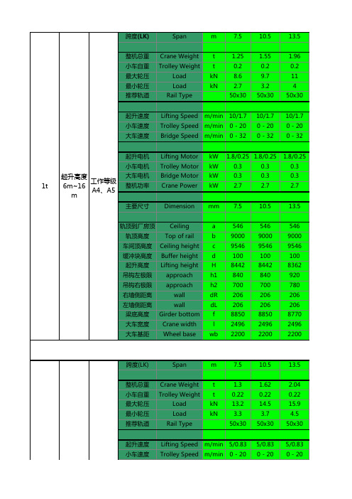
1.96 0.2 11 4 50x30
起升速度 小车速度 大车速度
Lifting Speed Trolley Speed Bridge Speed
m/min m/min m/min
10/1.7 0 - 20 0 - 32
10/1.7 0 - 20 0 - 32
10/1.7 0 - 20 0 - 32
9000 9546 100 8490 910 750 206 206 8844 2496 2200
9000 9646 100 8490 910 750 206 206 8844 2496 2200
9000 9556 100 8420 980 820 206 206 8774 2496 2200
跨度(LK)
2.18 0.23 21.8 5.2 50x30
起升速度 小车速度 大车速度
Lifting Speed m/min 5/0.83 Trolley Speed m/min 0 - 20 Bridge Speed m/min 0 - 32
5/0.83 0 - 20 0 - 32
5/0.83 0 - 20 0 - 32
轨顶高度
Top of rail
b
车间顶高度 Ceiling height c
缓冲块高度 Buffer height d
起升高度 Lifting height H
吊钩左极限 Hook approach h1
吊钩右极限 Hook approach h2
右墙侧距离 Rail center - wall dR
推荐轨道
Rail Type
1.97 0.61 33.8 7.4 P22
2.49 0.61 36.5 7.4 P22
CTDD2210SF-1215-D1.5K-2中文资料
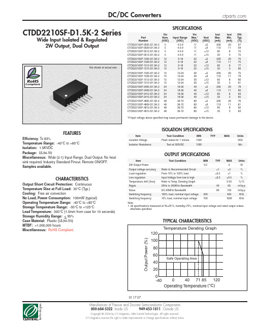
SPECIFICATIONSVin Vin Iout Iout Effi.Part Nom.Input RangeMax.*Vout Max.Min.Typ.Number(VDC)(VDC)(VDC)(VDC)(mA)(mA)(%)CTDD2210SF-0505-D1.5K-25 4.5-911±52002067CTDD2210SF-0509-D1.5K-25 4.5-911±91101169CTDD2210SF-0512-D1.5K-25 4.5-911±1283872CTDD2210SF-0515-D1.5K-25 4.5-911±1533375CTDD2210SF-1205-D1.5K-2129-1822±52002075CTDD2210SF-1209-D1.5K-2129-1822±91101175CTDD2210SF-1212-D1.5K-2129-1822±1283877CTDD2210SF-1215-D1.5K-2129-1822±1533380CTDD2210SF-1505-D1.5K-21512-2430±52002075CTDD2210SF-1509-D1.5K-21512-2430±91101179CTDD2210SF-1512-D1.5K-21512-2430±1283880CTDD2210SF-1515-D1.5K-21512-2430±1533381CTDD2210SF-2405-D1.5K-22418-3640±52002078CTDD2210SF-2409-D1.5K-22418-3640±91101180CTDD2210SF-2412-D1.5K-22418-3640±1283883CTDD2210SF-2415-D1.5K-22418-3640±1533385CTDD2210SF-4805-D1.5K-24836-7280±52002076CTDD2210SF-4809-D1.5K-24836-7280±91101181CTDD2210SF-4812-D1.5K-24836-7280±1283882CTDD2210SF-4815-D1.5K-24836-7280±1533383*If Input voltage above specified may cause permanent damage to the deviceISOLATION SPECIFICATIONSItem Test Condition MIN TYPMAXUnits Isolation Voltage Flash tested for 1 minute1500VDC Isolation ResistanceT est at 500VDC1000M ΩOUTPUT SPECIFICATIONSItem Test ConditionMIN TYPMAX Units 2W Output Power 0.22W Output voltage accuracy Refer to Recommended Circuit ±1±3%Load regulation From 10% to 100% load ±0.5±1%Line regulation Input Voltage from low to high ±0.2±0.5%T emperature drift (Vout)Refer to T emp.Derating Graph 0.03%/°C Ripple 20Hz to 300KHz Bandwidth 4060mVp-p NoiseDC-20MHz Bandwidth80150mVp-p Switching frequency 100% load, nominal input voltage 200400KHz Switching frequency10% load, nominal input voltage7001000KHzCTDD2210SF-D1.5K-2 SeriesWide Input Isolated & Regulated2W Output, Dual OutputNot shown at actual size.FEATURESEfficiency :T o 83%Temperature Range:-40°C to +85°C Isolation: 1.5KVDC Package:UL94-V0Miscellaneous:Wide (2:1) Input Range.Dual Output.No heat sink required.Industry Standard Pinout.Remote ON/OFF .Samples available.Output Short Circuit Protection:Continuous Temperature Rise at Full Load:30°C (T yp.)Cooling:Free air convectionNo Load,Power Consumption:100mW (typical)Operating Temperature Range:-40°C to +85°C Storage Temperature Range:-55°C to +125°CLead Temperature:300°C (1.5mm from case for 10 seconds)Storage Humidity Range:<95%Case Material:Plastic (UL94-V0)MTBF:>1,000,000 hoursMiscellaneous:RoHS Compliant.Note:1.All specifications measured at T A=25°C, humidity<75%, nominal input voltage and rated output unless otherwise specified.120806040u t p u t P o w e r (%)100Safe Operating AreaRoHSCompliantTemperature Derating GraphOUTLINE DIMENSIONS & RECOMMENDED FOOTPRINT DETAILS123567822.0012.0017.78 2.109.502.542.54ø1.00+0.15/-01.50Note: All Pin s on a 2.54mm pitch; All Pin di a meter s a re 0.50mm (T oler a nce: ±0.10); a ll dimen s ion s in mm..CTDD2210S F-D1.5K-2 P a ck a gePIN CONNECTIONS1 2 3 5 6 7 8Pin 1235678F u nction GND Vin CTRL NC +Vo OV -VoCTRLWhen open or high impedance, converter work well. When control pin positive referenced to the negative input (equal to import to earth), converter shutdown. Please note that the input current should be between 5-10mA, exeeding the maximum 20mA will cause permanent damage to converter.CTDD2210SF-D1.5K-2 SeriesWide Input Isolated & Regulated2W Output, Dual Outputlpn t (A )Figure 2Vin C in C o u t (0+70°C)C o u t (-40+85°C)5V &100µF100µF 47µF All the CTDD2210S F-D1.5K-2 S erie s h a ve b een te s ted a ccording to the following recommended te s ting circ u it b efore le a ving f a ctory . Thi s s erie s s ho u ld b e te s ted u nder lo a d. Never b e te s ted u nder no lo a d (S ee fig u re 1). If yo u w a nt to f u rther decre as e the inp u t/o u tp u t ripple, yo u c a n incre as c a p a cit a nce properly or choo s e c a p a citor s with low E S R. However, the c a p a cit a nce s ho u ld not b e too high (S ee t ab le 1). If yo u w a nt to us e the prod u ct s in high EMI, ple as e choo s e o u r met a l p a ck a ged prod u ct s .Fig u re 1Extern a l C a p a citor T ab le (t ab le 1)+++DC-DC +VinCinCo u t(5-10mA)2763+Vo 0V RECOMMENDED CIRCUIT。
MX25L1605DM2I-12G中文资料
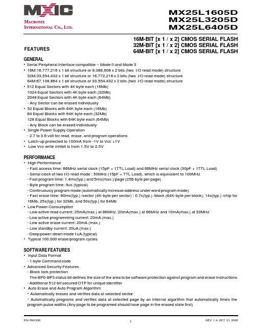
16M-BIT [x 1 / x 2] CMOS SERIAL FLASH 32M-BIT [x 1 / x 2] CMOS SERIAL FLASH 64M-BIT [x 1 / x 2] CMOS SERIAL FLASHFEATURESGENERAL• Serial Peripheral Interface compatible -- Mode 0 and Mode 3• 16M:16,777,216 x 1 bit structure or 8,388,608 x 2 bits (two I/O read mode) structure 32M:33,554,432 x 1 bit structure or 16,772,216 x 2 bits (two I/O read mode) structure 64M:67,108,864 x 1 bit structure or 33,554,432 x 2 bits (two I/O read mode) structure • 512 Equal Sectors with 4K byte each (16Mb)1024 Equal Sectors with 4K byte each (32Mb)2048 Equal Sectors with 4K byte each (64Mb)- Any Sector can be erased individually•32 Equal Blocks with 64K byte each (16Mb)64 Equal Blocks with 64K byte each (32Mb)128 Equal Blocks with 64K byte each (64Mb)- Any Block can be erased individually • Single Power Supply Operation- 2.7 to 3.6 volt for read, erase, and program operations • Latch-up protected to 100mA from -1V to Vcc +1V • Low Vcc write inhibit is from 1.5V to 2.5VPERFORMANCE • High Performance- Fast access time: 86MHz serial clock (15pF + 1TTL Load) and 66MHz serial clock (30pF + 1TTL Load)- Serial clock of two I/O read mode : 50MHz (15pF + TTL Load), which is equivalent to 100MHz - Fast program time: 1.4ms(typ.) and 5ms(max.)/page (256-byte per page)- Byte program time: 9us (typical)- Continuously program mode (automatically increase address under word program mode)- Fast erase time: 60ms(typ.) /sector (4K-byte per sector) ; 0.7s(typ.) /block (64K-byte per block); 14s(typ.) /chip for 16Mb, 25s(typ.) for 32Mb, and 50s(typ.) for 64Mb • Low Power Consumption- Low active read current: 25mA(max.) at 86MHz, 20mA(max.) at 66MHz and 10mA(max.) at 33MHz - Low active programming current: 20mA (max.)- Low active erase current: 20mA (max.)- Low standby current: 20uA (max.)- Deep power-down mode 1uA (typical)• Typical 100,000 erase/program cyclesSOFTWARE FEATURES • Input Data Format- 1-byte Command code •Advanced Security Features - Block lock protectionThe BP0-BP3 status bit defines the size of the area to be software protection against program and erase instructions - Additional 512-bit secured OTP for unique identifier • Auto Erase and Auto Program Algorithm- Automatically erases and verifies data at selected sector- Automatically programs and verifies data at selected page by an internal algorithm that automatically times the program pulse widths (Any page to be programed should have page in the erased state first)MX25L1605D MX25L3205D MX25L6405D元器件交易网•Status Register Feature•Electronic Identification- JEDEC 1-byte manufacturer ID and 2-byte device ID- RES command for 1-byte Device ID- Both REMS and REMS2 commands for 1-byte manufacturer ID and 1-byte device IDHARDWARE FEATURES• SCLK Input- Serial clock input• SI Input- Serial Data Input• SO Output- Serial Data Output• WP#/ACC pin- Hardware write protection and program/erase acceleration• HOLD# pin- pause the chip without diselecting the chip• PACKAGE- 16-pin SOP (300mil)- 8-land WSON (8x6mm or 6x5mm)- 8-pin SOP (200mil, 150mil)- 8-pin PDIP (300mil)- 8-land USON (4x4mm)- All Pb-free devices are RoHS CompliantALTERNATIVE• Security Serial Flash (MX25L1615D/MX25L3215D/MX25L6415D) may provides additional protection features for op-tion. The datasheet is provided under NDA.GENERAL DESCRIPTIONThe MX25L1605D are 16,777,216 bit serial Flash memory, which is configured as 2,097,152 x 8 internally. When it is in two I/O read mode, the structure becomes 8,388,608 bits x 2. The MX25L3205D are 33,554,432 bit serial Flash memory, which is configured as 4,194,304 x 8 internally. When it is in two I/O read mode, the structure becomes 16,772,216 bits x 2. The MX25L6405D are 67,108,864 bit serial Flash memory, which is configured as 8,388,608 x 8 internally. When it is in two I/O read mode, the structure becomes 33,554,432 bits x 2. (please refer to the "Two I/O Read mode" section). The MX25L1605D/3205D/6405D feature a serial peripheral interface and software protocol allowing operation on a simple 3-wire bus. The three bus signals are a clock input (SCLK), a serial data input (SI), and a serial data output (SO). Serial access to the device is enabled by CS# input.When it is in two I/O read mode, the SI pin and SO pin become SIO0 pin and SIO1 pin for address/dummy bits input and data output.The MX25L1605D/3205D/6405D provides sequential read operation on whole chip.After program/erase command is issued, auto program/ erase algorithms which program/ erase and verify the specified page or sector/block locations will be executed. Program command is executed on byte basis, or page (256 bytes) basis, or word basis for Continuously program mode, and erase command is executes on sector (4K-byte), or block (64K-byte), or whole chip basis.To provide user with ease of interface, a status register is included to indicate the status of the chip. The status read command can be issued to detect completion status of a program or erase operation via WIP bit.Advanced security features enhance the protection and security functions, please see security features section for more details.When the device is not in operation and CS# is high, it is put in standby mode and draws less than 20uA DC current. The MX25L1605D/3205D/6405D utilizes MXIC's proprietary memory cell, which reliably stores memory contents even after typical 100,000 program and erase cycles.Table 1. Additional Feature ComparisonPIN CONFIGURATIONSSYMBOL DESCRIPTION CS#Chip SelectSI/SIO0Serial Data Input (for 1 x I/O)/ Serial Data Input & Output (for 2xI/O read mode)SO/SIO1Serial Data Output (for 1 x I/O)/ Serial Data Input & Output (for 2xI/O read mode)SCLK Clock InputWP#/ACCWrite protection: connect to GND ;9.5~10.5V for program/eraseacceleration: connect to 9.5~10.5V HOLD#Hold, to pause the device without deselecting the device VCC + 3.3V Power Supply GNDGroundPIN DESCRIPTION16-PIN SOP (300mil)8-LAND WSON (8x6mm, 6x5mm), USON (4x4mm)8-PIN SOP (200mil, 150mil)PACKAGE OPTIONS16M 32M 64M150mil 8-SOP V 200mil 8-SOP V V 300mil 16-SOP V V V300mil 8-PDIP V V 6x5mm WSON V V 8x6mm WSON V4x4mm USONVV12345678HOLD#VCC NC NC NC NC CS#SO/SIO1161514131211109SCLK SI/SIO0NC NC NC NC GND WP#/ACCCS#SO/SIO1WP#/ACCGND VCC HOLD#SCLK SI/SIO0CS#SO/SIO1WP#/ACC GND VCC HOLD#SCLK SI/SIO01234CS#SO/SIO1WP#/ACC GND 8765VCC HOLD#SCLK SI/SIO08-PIN PDIP (300mil)BLOCK DIAGRAMDATA PROTECTIONThe MX25L1605D/3205D/6405D is designed to offer protection against accidental erasure or programming caused by spurious system level signals that may exist during power transition. During power up the device automatically resets the state machine in the Read mode. In addition, with its control register architecture, alteration of the memory contents only occurs after successful completion of specific command sequences. The device also incorporates several features to prevent inadvertent write cycles resulting from VCC power-up and power-down transition or system noise.•Power-on reset and tPUW: to avoid sudden power switch by system power supply transition, the power-on reset and tPUW (internal timer) may protect the Flash.• Valid command length checking: The command length will be checked whether it is at byte base and completed on byte boundary.• Write Enable (WREN) command: WREN command is required to set the Write Enable Latch bit (WEL) before other command to change data. The WEL bit will return to reset stage under following situation:- Power-up- Write Disable (WRDI) command completion- Write Status Register (WRSR) command completion- Page Program (PP) command completion- Continuously Program mode (CP) instruction completion- Sector Erase (SE) command completion- Block Erase (BE) command completion- Chip Erase (CE) command completion- Write Read-lock Bit (WRLB) instruction completion•Deep Power Down Mode: By entering deep power down mode, the flash device also is under protected from writing all commands except Release from deep power down mode command (RDP) and Read Electronic Signature command (RES).•Advanced Security Features: there are some protection and securuity features which protect content from inadvertent write and hostile access.I. Block lock protection- The Software Protected Mode (SPM) use (BP3, BP2, BP1, BP0) bits to allow part of memory to be protected as read only. The proected area definition is shown as table of "Protected Area Sizes", the protected areas are more flexible which may protect various area by setting value of BP0-BP3 bits.Please refer to table of "protected area sizes".- The Hardware Proteced Mode (HPM) use WP#/ACC to protect the (BP3, BP2, BP1, BP0) bits and SRWD bit.Table 2. Protected Area SizesII. Additional 512-bit secured OTP for unique identifier: to provide 512-bit one-time program area for setting device unique serial number - Which may be set by factory or system customer. Please refer to table 3. 512-bit secured OTP definition.- Security register bit 0 indicates whether the chip is locked by factory or not.- To program the 512-bit secured OTP by entering 512-bit secured OTP mode (with ENSO command), and going through normal program procedure, and then exiting 512-bit secured OTP mode by writing EXSO command.- Customer may lock-down the customer lockable secured OTP by writing WRSCUR(write security register) command to set customer lock-down bit1 as "1". Please refer to table of "security register definition" for security register bit definition and table of "512-bit secured OTP definition" for address range definition.- Note: Once lock-down whatever by factory or customer, it cannot be changed any more. While in 512-bit secured OTP mode, array access is not allowed.Table 3. 512-bit Secured OTP DefinitionAddress range Size Standard Customer LockFactory Lockxxxx00~xxxx0F128-bit ESN (electrical serial number)Determined by customer xxxx10~xxxx3F384-bit N/AHOLD FEATURESHOLD# pin signal goes low to hold any serial communications with the device. The HOLD feature will not stop the operation of write status register, programming, or erasing in progress.The operation of HOLD requires Chip Select(CS#) keeping low and starts on falling edge of HOLD# pin signal while Serial Clock (SCLK) signal is being low (if Serial Clock signal is not being low, HOLD operation will not start until Serial Clock signal being low). The HOLD condition ends on the rising edge of HOLD# pin signal while Serial Clock(SCLK) signal is being low( if Serial Clock signal is not being low, HOLD operation will not end until Serial Clock being low), see Figure 1. Figure 1. Hold Condition OperationThe Serial Data Output (SO) is high impedance, both Serial Data Input (SI) and Serial Clock (SCLK) are don't care during the HOLD operation. If Chip Select (CS#) drives high during HOLD operation, it will reset the internal logic of the device. To re-start communication with chip, the HOLD# must be at high and CS# must be at low.PROGRAM/ERASE ACCELERATIONTo activate the program/erase acceleration function requires ACC pin connecting to 9.5~10.5V voltage (see Figure 2), and then to be followed by the normal program/erase process. By utilizing the program/erase acceleration operation, the performances are improved as shown on table of "ERASE AND PROGRAM PERFORMACE".After power-up ready, it should wait 10ms at least to apply VHH(9.5~10.5V) on the WP#/ACC pin.Figure 2. ACCELERATED PROGRAM TIMING DIAGRAMNote: tVHH (VHH Rise and Fall Time) min. 250nsTable 4. COMMAND DEFINITIONCOMMAND (byte)WREN (writeenable)WRDI (write disable)RDID (read identification )RDSR (read statusregister)WRSR(write status register)READ (read data)FAST READ(fast read data)2READ (2x I/O read command)note1SE (sector erase)1st byte 06 (hex)04 (hex)9F (hex)05 (hex)01 (hex)03 (hex)0B (hex)BB (hex)20 (hex)2nd byte AD1AD1ADD(2)AD13rd byte AD2AD2ADD(2) &Dummy(2)AD24th byte AD3AD3AD35th byte Actionsets the (WEL)write enable latch bit resets the (WEL)write enable latch bitoutputs JEDEC ID:1-byte manufactur er ID & 2-byte device IDto read out the values of the status register to writenew values to the statusregister n bytes read out until CS#goes high n bytes read out until CS#goes high n bytes read out by 2 x I/O until CS#goes high to erase the selectedsector Note 1: The count base is 4-bit for ADD(2) and Dummy(2) because of 2 x I/O. And the MSB is on SI/SIO0 which is different from 1 x I/O conditionCOMMAND (byte)BE (block erase)CE (chip erase)PP (Page program)CP (Continuo-usly program mode)DP (Deep powerdown)RDP (Release from deep power down)RES (read electronic ID)REMS(read electronic manufactu-rer &device ID)REMS2(read ID for 2x I/O mode)1st byte D8 (hex)60 or C7(hex)02 (hex)AD (hex)B9 (hex)AB (hex)AB (hex)90 (hex)EF (hex)2nd byte AD1AD1AD1x x x 3rd byte AD2AD2AD2x x x 4th byte AD3AD3AD3x ADD(note 2)ADD(note2)5th byteAction to erase theselected block to erase whole chip to program the selected page continously program wholechip, theaddress is automatica lly increaseentersdeep power down moderelease from deep power down mode to read out 1-byte device ID outout the manufactu-rer ID &device ID output the manufactu-rer ID &device ID Note 2: ADD=00H will output the manufacturer ID first and ADD=01H will output device ID first Note 3: It is not recommoded to adopt any other code not in the command definition table, which will potentially enter the hidden mode.COMMAND (byte)ENSO (enter secured OTP)EXSO (exit secured OTP)RDSCUR (read security register)WRSCUR (write security register)ESRY (enable SO to output RY/BY#)DSRY (disable SO to output RY/BY#)1st byte B1 (hex)C1 (hex)2B (hex)2F (hex)70 (hex)80 (hex)2nd byte 3rd byte 4th byte 5th byte Actionto enter the 512-bit secured OTP mode to exit the 512-bit secured OTP mode to read value of security registerto set the lock-down bit as "1"(once lock-down,cannot be updated)to enable SO to output RY/BY#during CP mode to disable SO to output RY/BY#during CP modeDummyTable 5-1. Memory Organization (16Mb)Table 5-2. Memory Organization (32Mb)Table 5-3. Memory Organization (64Mb)DEVICE OPERATION1.Before a command is issued, status register should be checked to ensure device is ready for the intended operation.2.When incorrect command is inputted to this LSI, this LSI becomes standby mode and keeps the standby mode until next CS# falling edge. In standby mode, SO pin of this LSI should be High-Z.3.When correct command is inputted to this LSI, this LSI becomes active mode and keeps the active mode until next CS# rising edge.4.Input data is latched on the rising edge of Serial Clock(SCLK) and data shifts out on the falling edge of SCLK. The difference of Serial mode 0 and mode 3 is shown as Figure 3.Figure 3. Serial Modes Supported5.For the following instructions: RDID, RDSR, RDSCUR, READ, FAST_READ, 2READ, RES, REMS and REMS2 the shifted-in instruction sequence is followed by a data-out sequence. After any bit of data being shifted out, the CS# can be high. For the following instructions: WREN, WRDI, WRSR, SE, BE, CE, PP, CP, RDP, DP, ENSO, EXSO,and WRSCUR, the CS# must go high exactly at the byte boundary; otherwise, the instruction will be rejected and not executed.6.During the progress of Write Status Register, Program, Erase operation, to access the memory array is neglected and not affect the current operation of Write Status Register, Program, Erase.Note:CPOL indicates clock polarity of Serial master, CPOL=1 for SCLK high while idle, CPOL=0 for SCLK low while not transmitting. CPHA indicates clock phase. The combination of CPOL bit and CPHA bit decides which Serial mode is supported.SCLKMSBCPHASI 01CPOL 0(Serial mode 0)(Serial mode 3)1SO SCLKMSBCOMMAND DESCRIPTION(1) Write Enable (WREN)The Write Enable (WREN) instruction is for setting Write Enable Latch (WEL) bit. For those instructions like PP, CP, SE, BE, CE, and WRSR, which are intended to change the device content, should be set every time after the WREN instruction setting the WEL bit.The sequence of issuing WREN instruction is: CS# goes low-> sending WREN instruction code-> CS# goes high. (see Figure 12)(2) Write Disable (WRDI)The Write Disable (WRDI) instruction is for resetting Write Enable Latch (WEL) bit.The sequence of issuing WRDI instruction is: CS# goes low-> sending WRDI instruction code-> CS# goes high. (see Figure 13)The WEL bit is reset by following situations:- Power-up- Write Disable (WRDI) instruction completion- Write Status Register (WRSR) instruction completion- Page Program (PP) instruction completion- Sector Erase (SE) instruction completion- Block Erase (BE) instruction completion- Chip Erase (CE) instruction completion- Continuously program mode (CP) instruction completion(3) Read Identification (RDID)The RDID instruction is for reading the manufacturer ID of 1-byte and followed by Device ID of 2-byte. The MXIC Manufacturer ID is C2(hex), the memory type ID is 20(hex) as the first-byte device ID, and the individual device ID of second-byte ID are listed as table of "ID Definitions".The sequence of issuing RDID instruction is: CS# goes low-> sending RDID instruction code -> 24-bits ID data out on SO -> to end RDID operation can use CS# to high at any time during data out. (see Figure. 14)While Program/Erase operation is in progress, it will not decode the RDID instruction, so there's no effect on the cycle of program/erase operation which is currently in progress. When CS# goes high, the device is at standby stage.(4) Read Status Register (RDSR)The RDSR instruction is for reading Status Register Bits. The Read Status Register can be read at any time (even in program/erase/write status register condition) and continuously. It is recommended to check the Write in Progress (WIP) bit before sending a new instruction when a program, erase, or write status register operation is in progress.The sequence of issuing RDSR instruction is: CS# goes low-> sending RDSR instruction code-> Status Register data out on SO (see Figure. 15)The definition of the status register bits is as below:WIP bit. The Write in Progress (WIP) bit, a volatile bit, indicates whether the device is busy in program/erase/write status register progress. When WIP bit sets to 1, which means the device is busy in program/erase/write status register progress. When WIP bit sets to 0, which means the device is not in progress of program/erase/write status register cycle.WEL bit. The Write Enable Latch (WEL) bit, a volatile bit, indicates whether the device is set to internal write enable latch. When WEL bit sets to 1, which means the internal write enable latch is set, the device can accept program/erase/write status register instruction. When WEL bit sets to 0, which means no internal write enable latch; the device will not accept program/erase/write status register instruction. The program/erase command will be ignored and not affect value of WEL bit if it is applied to a protected memory area.BP3, BP2, BP1, BP0 bits. The Block Protect (BP3, BP2, BP1, BP0) bits, non-volatile bits, indicate the protected area(as defined in table 1) of the device to against the program/erase instruction without hardware protection mode being set. To write the Block Protect (BP3, BP2, BP1, BP0) bits requires the Write Status Register (WRSR) instruction to be executed. Those bits define the protected area of the memory to against Page Program (PP), Sector Erase (SE), Block Erase (BE) and Chip Erase(CE) instructions (only if all Block Protect bits set to 0, the CE instruction can be executed).Continuously Program Mode( CP mode) bit. The Continuously Program Mode bit indicates the status of CP mode, "0" indicates not in CP mode; "1" indicates in CP mode.SRWD bit. The Status Register Write Disable (SRWD) bit, non-volatile bit, is operated together with Write Protection (WP#/ ACC) pin for providing hardware protection mode. The hardware protection mode requires SRWD sets to 1 and WP#/ACC pin signal is low stage. In the hardware protection mode, the Write Status Register (WRSR) instruction is no longer accepted for execution and the SRWD bit and Block Protect bits (BP3, BP2, BP1, BP0) are read only.Status Registernote1: see the table "Protected Area Sizes"(5) Write Status Register (WRSR)The WRSR instruction is for changing the values of Status Register Bits. Before sending WRSR instruction, the Write Enable (WREN) instruction must be decoded and executed to set the Write Enable Latch (WEL) bit in advance. The WRSR instruction can change the value of Block Protect (BP3, BP2, BP1, BP0) bits to define the protected area of memory (as shown in table 1). The WRSR also can set or reset the Status Register Write Disable (SRWD) bit in accordance with Write Protection (WP#/ACC) pin signal. The WRSR instruction cannot be executed once the Hardware Protected Mode (HPM)is entered.The sequence of issuing WRSR instruction is: CS# goes low-> sending WRSR instruction code-> Status Register data on SI-> CS# goes high. (see Figure 16)The WRSR instruction has no effect on b6, b1, b0 of the status register.The CS# must go high exactly at the byte boundary; otherwise, the instruction will be rejected and not executed. The self-timed Write Status Register cycle time (tW) is initiated as soon as Chip Select (CS#) goes high. The Write in Progress (WIP) bit still can be check out during the Write Status Register cycle is in progress. The WIP sets 1 during the tW timing,and sets 0 when Write Status Register Cycle is completed, and the Write Enable Latch (WEL) bit is reset.Table 6. Protection ModesNote:1. As defined by the values in the Block Protect (BP3, BP2, BP1, BP0) bits of the Status Register, as shown in Table 1.As the above table showing, the summary of the Software Protected Mode (SPM) and Hardware Protected Mode (HPM).Software Protected Mode (SPM):-When SRWD bit=0, no matter WP#/ACC is low or high, the WREN instruction may set the WEL bit and can changethe values of SRWD, BP3, BP2, BP1, BP0. The protected area, which is defined by BP3, BP2, BP1, BP0, is at software protected mode (SPM).-When SRWD bit=1 and WP#/ACC is high, the WREN instruction may set the WEL bit can change the values of SRWD,BP3, BP2, BP1, BP0. The protected area, which is defined by BP3, BP2, BP1, BP0, is at software protected mode (SPM)ModeStatus register condition Software protection mode(SPM)Status register can be written in (WEL bit is set to "1") and the SRWD, BP0-BP3bits can be changedWP# and SRWD bit status MemoryWP#=1 and SRWD bit=0, or WP#=0 and SRWD bit=0, or WP#=1 and SRWD=1The protected area cannot be program or erase.The protected area cannot be program or erase.WP#=0, SRWD bit=1The SRWD, BP0-BP3 ofstatus register bits cannot be changedHardware protection mode (HPM)Note: If SRWD bit=1 but WP#/ACC is low, it is impossible to write the Status Register even if the WEL bit has previously been set. It is rejected to write the Status Register and not be executed.Hardware Protected Mode (HPM):-When SRWD bit=1, and then WP#/ACC is low (or WP#/ACC is low before SRWD bit=1), it enters the hardware protected mode (HPM). The data of the protected area is protected by software protected mode by BP3, BP2, BP1, BP0 and hardware protected mode by the WP#/ACC to against data modification.Note: to exit the hardware protected mode requires WP#/ACC driving high once the hardware protected mode is entered. If the WP#/ACC pin is permanently connected to high, the hardware protected mode can never be entered; only can use software protected mode via BP3, BP2, BP1, BP0.(6) Read Data Bytes (READ)The read instruction is for reading data out. The address is latched on rising edge of SCLK, and data shifts out on the falling edge of SCLK at a maximum frequency fR. The first address byte can be at any location. The address is automatically increased to the next higher address after each byte data is shifted out, so the whole memory can be read out at a single READ instruction. The address counter rolls over to 0 when the highest address has been reached.The sequence of issuing READ instruction is: CS# goes low-> sending READ instruction code-> 3-byte address on SI -> data out on SO-> to end READ operation can use CS# to high at any time during data out. (see Figure. 17)(7) Read Data Bytes at Higher Speed (FAST_READ)The FAST_READ instruction is for quickly reading data out. The address is latched on rising edge of SCLK, and data of each bit shifts out on the falling edge of SCLK at a maximum frequency fC. The first address byte can be at any location. The address is automatically increased to the next higher address after each byte data is shifted out, so the whole memory can be read out at a single FAST_READ instruction. The address counter rolls over to 0 when the highest address has been reached.The sequence of issuing FAST_READ instruction is: CS# goes low-> sending FAST_READ instruction code-> 3-byte address on SI-> 1-dummy byte address on SI->data out on SO-> to end FAST_READ operation can use CS# to high at any time during data out. (see Figure. 18)While Program/Erase/Write Status Register cycle is in progress, FAST_READ instruction is rejected without any impact on the Program/Erase/Write Status Register current cycle.(8) 2 x I/O Read Mode (2READ)The 2READ instruction enable double throughput of Serial Flash in read mode. The address is latched on rising edge of SCLK, and data of every two bits(interleave on 2 I/O pins) shift out on the falling edge of SCLK at a maximum frequency fT. The first address byte can be at any location. The address is automatically increased to the next higher address after each byte data is shifted out, so the whole memory can be read out at a single 2READ instruction. The address counter rolls over to 0 when the highest address has been reached. Once writing 2READ instruction, the following address/dummy/ data out will perform as 2-bit instead of previous 1-bit.The sequence of issuing 2READ instruction is: CS# goes low→ sending 2READ instruction→ 24-bit address interleave on SIO1 & SIO0→ 8-bit dummy interleave on SIO1 & SIO0→ data out interleave on SIO1 & SIO0→ to end 2READ operation can use CS# to high at any time during data out (see Figure of 2 x I/O Read Mode Timing Waveform)While Program/Erase/Write Status Register cycle is in progress, 2READ instruction is rejected without any impact on the Program/Erase/Write Status Register current cycle.The 2 I/O only perform read operation. Program/Erase /Read ID/Read status/Read ID....operation do not support 2 I/O throughputs.(9) Sector Erase (SE)The Sector Erase (SE) instruction is for erasing the data of the chosen sector to be "1". The instruction is used for any 4K-byte sector. A Write Enable (WREN) instruction must execute to set the Write Enable Latch (WEL) bit before sending the Sector Erase (SE). Any address of the sector (see table 3) is a valid address for Sector Erase (SE) instruction. The CS# must go high exactly at the byte boundary (the latest eighth of address byte been latched-in); otherwise, the instruction will be rejected and not executed.Address bits [Am-A12] (Am is the most significant address) select the sector address.The sequence of issuing SE instruction is: CS# goes low -> sending SE instruction code-> 3-byte address on SI -> CS# goes high. (see Figure 22)The self-timed Sector Erase Cycle time (tSE) is initiated as soon as Chip Select (CS#) goes high. The Write in Progress (WIP) bit still can be check out during the Sector Erase cycle is in progress. The WIP sets 1 during the tSE timing, and sets 0 when Sector Erase Cycle is completed, and the Write Enable Latch (WEL) bit is reset. If the page is protected by BP3, BP2, BP1, BP0 bits, the Sector Erase (SE) instruction will not be executed on the page.(10) Block Erase (BE)The Block Erase (BE) instruction is for erasing the data of the chosen block to be "1". The instruction is used for 64K-byte sector erase operation. A Write Enable (WREN) instruction must execute to set the Write Enable Latch (WEL) bit before sending the Block Erase (BE). Any address of the block (see table 3) is a valid address for Block Erase (BE) instruction. The CS# must go high exactly at the byte boundary (the latest eighth of address byte been latched-in); otherwise, the instruction will be rejected and not executed.The sequence of issuing BE instruction is: CS# goes low -> sending BE instruction code-> 3-byte address on SI -> CS# goes high. (see Figure 23)The self-timed Block Erase Cycle time (tBE) is initiated as soon as Chip Select (CS#) goes high. The Write in Progress (WIP) bit still can be check out during the Sector Erase cycle is in progress. The WIP sets 1 during the tBE timing, and sets 0 when Sector Erase Cycle is completed, and the Write Enable Latch (WEL) bit is reset. If the page is protected by BP3, BP2, BP1, BP0 bits, the Block Erase (BE) instruction will not be executed on the page.(11) Chip Erase (CE)The Chip Erase (CE) instruction is for erasing the data of the whole chip to be "1". A Write Enable (WREN) instruction must execute to set the Write Enable Latch (WEL) bit before sending the Chip Erase (CE). Any address of the sector (see table 3) is a valid address for Chip Erase (CE) instruction. The CS# must go high exactly at the byte boundary( the latest eighth of address byte been latched-in); otherwise, the instruction will be rejected and not executed.The sequence of issuing CE instruction is: CS# goes low-> sending CE instruction code-> CS# goes high. (see Figure 24)。
低速货车型号识别汇总

➢ 农用车知识
➢ 定义 ➢ 低速载货汽车(四轮农用运输车)型号 ➢ 三轮汽车 (三轮农用运输车)型号 ➢ 农用运输车特点
➢ 拖拉机知识
➢ 定义 ➢ 拖拉机型号 ➢ 拖拉机特点
1.4.1 农用车定义
农用运输车以柴油机为动力装置,中小吨位、中低速度,从事道路运 输的机动车辆。
➢ 农用运输车按其使用性质分为三轮汽车(原三轮农用运输车)和低速 载货汽车(原四轮农用运输车)。
低速载货汽车
产品型号名称 产品商标 外形尺寸(mm) 长*宽*高 功率(kw) 燃料种类 额定质量(kg) 整备质量(kg) 驾驶室准乘人数 (人)
发动机型号:
车辆新产品技术参数
HFC5820-1低速货车
HB1605-1低速货车
五叶牌
黑豹牌
5980 * 1990 * 2170
3935,4055 * 1415,1490 * 1835
➢ 形式代号采用下列数字符号:
➢ (空白) —一般农业用
G—果园用
H—高地隙中耕用
L—营林用
J—集柴用
P—坡地用
S—水田用
T—运输用
Y—园艺用
Z—沼泽地用
但是目前国产拖拉机大部分没有按照国家标准命名,而是各厂家自己命名,因此 国产拖拉机的型号比较乱,以上型号编制仅供参考。
1.4.7 拖拉机特点
➢ 拖拉机的发动机一般是以柴油为动力。农用型拖拉机常 见的动力有12马力,15马力,18马力,22马力,32马 力,40马力,50马力,60马力,80马力等,1马力等于 0.735千瓦。收割机一般是20马力以上。运输型拖拉机 一般马力比较大,大多数是20马力以上。发动机类型一 般有单缸,双缸,四缸,六缸等。
cTD500-15Kw变频器说明书
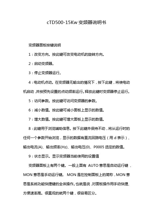
cTD500-15Kw变频器说明书变频器面板按键说明1:改变方向。
按此键可改变电动机的旋转方向。
2:启动变频器。
3:停止变频器运行。
4:电动机点动。
在变频器无输出的情况下,按下此键,将使电动机启动,并按预先设置的点动频率运行。
释放此键时变频器停止运行。
5:访问参数。
按此键可访问变频器的参数。
6:减小数值。
按此键可减小面板上显示的数值。
7:增大数值。
按此键可增大面板上显示的数值。
8:此键用于浏览辅助信息。
按下此键并保持不动,将从运行时的任何一个参数开始浏览,显示的数据有直流回路电压(用d表示)、输出电流(A)、输出频率(Hz)、输出电压(0)、P0005选定的数值。
9:状态显示。
显示变频器当前使用的设置值变频器面板上有两个键。
一般上面有AUTO意思是自动运行键、MON意思是手动运行键。
MON是在控制面板上的简称,MON意思是系统功能快捷键的全体操作。
也就是说,对面板操作用手动快捷、方便速率高。
很直观的就两个键,很容易区分。
变频器面板按键说明1:改变方向。
按此键可改变电动机的旋转方向。
2:启动变频器。
3:停止变频器运行。
4:电动机点动。
在变频器无输出的情况下,按下此键,将使电动机启动,并按预先设置的点动频率运行。
释放此键时变频器停止运行。
5:访问参数。
按此键可访问变频器的参数。
6:减小数值。
按此键可减小面板上显示的数值。
7:增大数值。
按此键可增大面板上显示的数值。
8:此键用于浏览辅助信息。
按下此键并保持不动,将从运行时的任何一个参数开始浏览,显示的数据有直流回路电压(用d表示)、输出电流(A)、输出频率(Hz)、输出电压(0)、P0005选定的数值。
9:状态显示。
显示变频器当前使用的设置值变频器面板上有两个键。
一般上面有AUTO意思是自动运行键、MON意思是手动运行键。
MON是在控制面板上的简称,MON意思是系统功能快捷键的全体操作。
也就是说,对面板操作用手动快捷、方便速率高。
很直观的就两个键,很容易区分。
DK125规格书
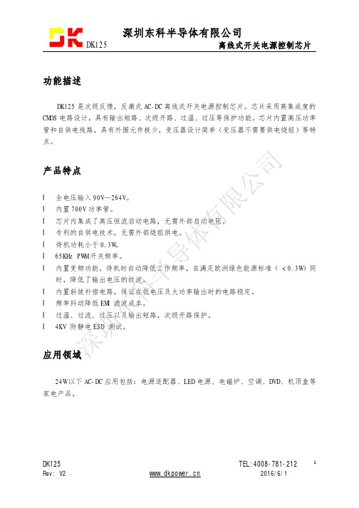
功能描述DK125是次级反馈,反激式AC-DC 离线式开关电源控制芯片。
芯片采用高集成度的CMOS 电路设计,具有输出短路、次级开路、过温、过压等保护功能。
芯片内置高压功率管和自供电线路,具有外围元件极少,变压器设计简单(变压器不需要供电绕组)等特点。
产品特点l 全电压输入90V —264V 。
l 内置700V 功率管。
l 芯片内集成了高压恒流启动电路,无需外部启动电阻。
l 专利的自供电技术,无需外部绕组供电。
l 待机功耗小于0.3W 。
l 65KHz PWM 开关频率。
l 内置变频功能,待机时自动降低工作频率,在满足欧洲绿色能源标准(<0.3W )同时,降低了输出电压的纹波。
l 内置斜坡补偿电路,保证在低电压及大功率输出时的电路稳定。
l 频率抖动降低EMI 滤波成本。
l 过温、过流、过压以及输出短路,次级开路保护。
l4KV 防静电ESD 测试。
应用领域24W 以下AC-DC 应用包括:电源适配器、LED 电源、电磁炉、空调、DVD 、机顶盒等家电产品。
深圳东科半导体有限公司封装与引脚定义(DIP8)内部框图引脚符号功能描述1GND 接地引脚2GND 接地引脚3FB反馈控制端引脚,接1nF ~10nF4VCC 供电引脚,外部对地接47uF ~100uF 的电容5,6,7,8OC输出引脚,连接芯片内高压功率管,外部与开关变压器相连深圳东科半导体有限公司极限参数供电电压VDD ………………………………………………………-0.3V--8V 供电电流VDD ………………………………………………………100mA引脚电压………………………………………………………-0.3V--VDD+0.3V 功率管耐压………………………………………………………-0.3V--700V 峰值电流………………………………………………………1300mA总耗散功率………………………………………………………1000mW工作温度………………………………………………………-25°C--+125°C 储存温度………………………………………………………-55°C--+150°C 焊接温度………………………………………………………+280°C/5S电气参数项目测试条件最小典型最大单位VCC 工作电压AC 输入85V-----265V 4.54.7 4.9V VCC 启动电压AC 输入85V-----265V 4.7V VCC 重启电压AC 输入85V-----265V 3.30 3.60 3.90V VCC 保护电压AC 输入85V-----265V 6.25 6.55 6.85V VCC 工作电流VCC=5V ,FB=1.5V 50mA 高压启动电流AC 输入85V-----265V0.30.6 1.2mA 启动时间AC 输入85V ------500mS 功率管耐压Ioc=1mA 700------V 功率管保护电压测量OC 电压540600660V 最大峰值电流VCC=5V ,FB=1.5V---2.8V 110012001300mA PWM 输出频率VCC=5V ,FB=1.5V---2.5V 616569KHz VCC=5V ,FB=2.5v-2.8v202224KHz 调制步进频率VCC=5V ,FB=1.5v-2.5v0.5KHz 短路保护阀值测量FB 电压 1.15 1.33 1.50V 变频阀值电压测量FB 电压 2.3 2.5 2.7V 突发模式阀值测量FB 电压2.6 2.83.0V温度保护结温120130140℃深圳东科半导体有限公司前沿消隐时间VCC=5V ,FB=1.5v-2.5v 250ns最小开通时间VCC=5V ,FB=2.6v 500ns 占空比VCC=5V ,FB=1.5v-2.5v 5---70%待机功耗AC 输入265V,空载270mW功能描述上电启动上电启动时,芯片通过内部连接OC 和VCC 引脚的高压电流源,对外部的VCC 储能电容充电,当VCC 电压升高到4.7V 的时候,关闭高压电流源,启动过程结束,控制逻辑开始输出PWM 脉冲。
聚宝奥峰牌农用车主要技术参数表公告

轮胎数
6
6
其它
备注
188批补反光标识,190批补油耗
188批补反光标识,190批补油耗
生产地址
山东省寿光市稻田镇
山东省寿光市稻田镇
“聚宝”、“奥峰”牌低速货车主要技术参数表(农国Ⅱ)
厂牌型号名称
JBC2315低速货车
JBC2315W低速货车
公告期数
202批20091215发布-189
202批20091215发布-195
-/6+5
★前/后轮距(mm)
-/1220
最高设计车速
49.9
额定载质量(kg)
490
★整备质量(kg)
1060(500/560)
★总质量(kg)
1680(650/1030)
○质量利用系数
/
接近角/离去角
-/28
轮轮胎规格(前/后)
5.00-16/6.50-16
发动机型号
ZS1110
缸径*行程
110*115
发动机生产企业
常柴股份有限公司
常柴股份有限公司
排量
1194
1194
▲功率/标定转速
16.2/2200
16.2/2200
排放依据标准
GB18322-2002,GB19756-2005(Ⅱ)
GB18322-2002,GB19756-2005(Ⅱ)
油耗
GB21378-2008
GB21378-2008
制动操作方式
JBC1405D1自卸低速货车
公告期数
190批20090514发布-188-160
190批20090514发布-188-160
对应公告产品号
NH7L32TK070
- 1、下载文档前请自行甄别文档内容的完整性,平台不提供额外的编辑、内容补充、找答案等附加服务。
- 2、"仅部分预览"的文档,不可在线预览部分如存在完整性等问题,可反馈申请退款(可完整预览的文档不适用该条件!)。
- 3、如文档侵犯您的权益,请联系客服反馈,我们会尽快为您处理(人工客服工作时间:9:00-18:30)。
SPECIFICATIONS
Vin Iout Iout Effi.Part Nom.Input Range
Vout Max.Min.Typ.Number
(VDC)(VDC)
(VDC)(mA)(mA)(%)CTDD1605SF-0303-SU1K-1 3.3 3.0-3.6 3.33003072CTDD1605SF-0305-SU1K-1 3.3 3.0-3.652002073CTDD1605SF-0503-SU1K-15 4.5-5.5 3.33003074CTDD1605SF-0505-SU1K-15 4.5-5.552002072CTDD1605SF-0509-SU1K-15 4.5-5.591111274CTDD1605SF-0512-SU1K-15 4.5-5.51283977CTDD1605SF-0515-SU1K-15 4.5-5.51567779CTDD1605SF-1203-SU1K-11210.8-13.2 3.33003075CTDD1605SF-1205-SU1K-11210.8-13.252002076CTDD1605SF-1209-SU1K-11210.8-13.291111275CTDD1605SF-1212-SU1K-11210.8-13.21283979CTDD1605SF-1215-SU1K-11210.8-13.21567780CTDD1605SF-2403-SU1K-12421.6-26.4 3.33003076CTDD1605SF-2405-SU1K-12421.6-26.452002074CTDD1605SF-2409-SU1K-12421.6-26.491111276CTDD1605SF-2412-SU1K-12421.6-26.41283980CTDD1605SF-2415-SU1K-1
24
21.6-26.4
15
67
7
81
ISOLATION SPECIFICATIONS
Item Test Condition MIN TYP
MAX
Units Isolation Voltage T ested for 1 minute 1000VDC Isolation Resistance
T est at 500VDC
1000
M Ω
OUTPUT SPECIFICATIONS
Item Test Condition
MIN TYP
MAX Units Output Power 0.1
1W Line regulation For Vin change of 1% 1.2%Load regulation 10% to 100% full load 15
%
Output voltage accuracy See tolerance envelope graph T emperature drift 100% full load 0.03%/°C Output ripple 20MHz bandwidth
5075
mVp-p Switching frequency
Full load, nominal input voltage
100
KHz
CTDD1605SF-SU1K-1 Series
Fixed Input Isolated & Unregulated
1W Output, Single Output
Not shown at actual size.
FEATURES
Efficiency :T o 81%
Temperature Range:-40°C to 85°C Isolation:1KVDC Package:UL94-V0
Miscellaneous:Single Output Voltage.No heatsink required.No external component required.Industry standard pinout.Small footprint.Custom service available.Samples available.
Short Circuit Protection: 1 second
Temperature Rise at Full Load:25°C Max.15°C T yp.Cooling:Free air convection
Operating Temperature Range:-40°C to +85°C Storage Temperature Range:-55°C to +125°C
Lead Temperature:300°C (1.5mm from case for 10 seconds)Storage Humidity Range:<95%Case Material:Plastic (UL94-V0)MTBF:>3,500,000 hours
Miscellaneous:RoHS Compliant.
Note:
1.All specifications measured at T A=25°C, humidity<75%, nominal input voltage and rated output unless otherwise specified.
TYPICAL CHARACTERISTICS
+10%Tolerance Envelope Graph Temperature Derating Graph
Safe Operating Area
10%50%100%
Output Current(%)+2.5%12060
40200-40
04080Ambient Temperature(°C)
O u t p u t P o w e r (%)
80100-2.5%-7.5%
T y p i c
a
l L o a d
L i n e
+5%Nominal Voltage
O u t p u t V o l t a g e (%)
RoHS
Compliant
OUTLINE DIMENSIONS & RECOMMENDED FOOTPRINT DETAILS
16.50
CTDD1605SF-SU1K-1Package
CTDD1605SF-SU1K-1Footprint
Note:All pins on a 2.54mm pitch;all pin diameters are 0.50mm;all dimensions in mm.
7.504.10
12 2.54
46
ø1.00+0.15/-0
2.54
5.80
Side View
Top View
PIN CONNECTIONS
1246Pin Function Vin GND 0V +Vo
1246
CTDD1605SF-SU1K-1 Series
Fixed Input Isolated &Unregulated
1W Output, Single Output。