1N5921A中文资料
1N5822RLG;1N5820RLG;1N5821RLG;1N5822G;1N5821G;中文规格书,Datasheet资料

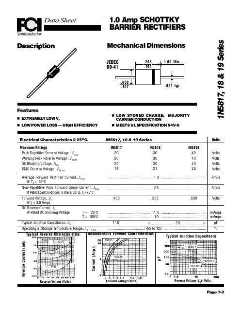
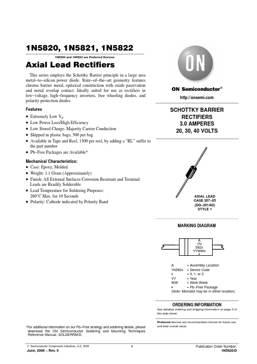
1N5820, 1N5821, 1N58221N5820 and 1N5822 are Preferred DevicesAxial Lead RectifiersThis series employs the Schottky Barrier principle in a large area metal-to-silicon power diode. State-of-the-art geometry features chrome barrier metal, epitaxial construction with oxide passivation and metal overlap contact. Ideally suited for use as rectifiers in low-voltage, high-frequency inverters, free wheeling diodes, and polarity protection diodes.Features•ăExtremely Low V F•ăLow Power Loss/High Efficiency•ăLow Stored Charge, Majority Carrier Conduction•ăShipped in plastic bags, 500 per bag•ăAvailable in Tape and Reel, 1500 per reel, by adding a “RL'' suffix tothe part number•ăPb-Free Packages are Available*Mechanical Characteristics:•ăCase: Epoxy, Molded•ăWeight: 1.1 Gram (Approximately)•ăFinish: All External Surfaces Corrosion Resistant and Terminal Leads are Readily Solderable•ăLead Temperature for Soldering Purposes:260°C Max. for 10 Seconds•ăPolarity: Cathode indicated by Polarity Band*For additional information on our Pb-Free strategy and soldering details, please download the ON Semiconductor Soldering and Mounting Techniques Reference Manual, SOLDERRM/D.CASE 267-05(DO-201AD)STYLE 1SCHOTTKY BARRIERRECTIFIERS3.0 AMPERES20, 30, 40 VOLTSPreferred devices are recommended choices for future use and best overall value.MARKING DIAGRAMSee detailed ordering and shipping information on page 3 of this data sheet.ORDERING INFORMATIONA= Assembly Location1N582x= Device Codex= 0, 1, or 2YY= YearWW= Work WeekG= Pb-Free Package(Note: Microdot may be in either location)A1N582xYYWW GGMAXIMUM RATINGSStresses exceeding Maximum Ratings may damage the device. Maximum Ratings are stress ratings only. Functional operation above the Recommended Operating Conditions is not implied. Extended exposure to stresses above the Recommended Operating Conditions may affect device reliability.*THERMAL CHARACTERISTICS (Note 5)Characteristic Symbol Max Unit Thermal Resistance, Junction-to-Ambient R q JA28°C/W*ELECTRICAL CHARACTERISTICS (T L = 25°C unless otherwise noted) (Note 1)Characteristic Symbol1N58201N58211N5822UnitMaximum Instantaneous Forward Voltage (Note 2) (i F = 1.0 Amp)(i F = 3.0 Amp)(i F = 9.4 Amp)V F0.3700.4750.8500.3800.5000.9000.3900.5250.950VMaximum Instantaneous Reverse Current @ Rated dc Voltage (Note 2)T L = 25°CT L = 100°C i R2.0202.0202.020mA1.Lead Temperature reference is cathode lead 1/32″ from case.2.Pulse Test: Pulse Width = 300 m s, Duty Cycle =2.0%.*Indicates JEDEC Registered Data for 1N5820-22.ORDERING INFORMATIONDevice Package Shipping†1N5820Axial Lead500 Units/Bag500 Units/Bag1N5820G Axial Lead(Pb-Free)1N5820RL Axial Lead1500/T ape & Reel1500/T ape & Reel1N5820RLG Axial Lead(Pb-Free)1N5821Axial Lead500 Units/Bag500 Units/Bag1N5821G Axial Lead(Pb-Free)1N5821RL Axial Lead1500/T ape & Reel1500/T ape & Reel1N5821RLG Axial Lead(Pb-Free)1N5822Axial Lead500 Units/Bag500 Units/Bag1N5822G Axial Lead(Pb-Free)1N5822RL Axial Lead1500/T ape & Reel1500/T ape & Reel1N5822RLG Axial Lead(Pb-Free)†For information on tape and reel specifications, including part orientation and tape sizes, please refer to our Tape and Reel Packaging Specifications Brochure, BRD8011/D.NOTE 3 — DETERMINING MAXIMUM RATINGSReverse power dissipation and the possibility of thermal runaway must be considered when operating this rectifier at reverse voltages above 0.1 V RWM. Proper derating may be accomplished by use of equation (1).T A(max) = T J(max)* R q JA P F(A V)* R q JA P R(A V)(1) where T A(max) = Maximum allowable ambient temperature T J(max) = Maximum allowable junction temperature(125°C or the temperature at which thermalrunaway occurs, whichever is lowest) P F(A V) = Average forward power dissipationP R(A V) = Average reverse power dissipationR q JA = Junction-to-ambient thermal resistance Figures 1, 2, and 3 permit easier use of equation (1) by taking reverse power dissipation and thermal runaway into consideration. The figures solve for a reference temperature as determined by equation (2).T R = T J(max)* R q JA P R(A V)(2) Substituting equation (2) into equation (1) yields:T A(max) = T R* R q JA P F(A V)(3) Inspection of equations (2) and (3) reveals that T R is the ambient temperature at which thermal runaway occurs or where T J = 125°C, when forward power is zero. The transition from one boundary condition to the other is evident on the curves of Figures 1, 2, and 3 as a difference in the rate of change of the slope in the vicinity of 115°C. The data of Figures 1, 2, and 3 is based upon dc conditions. For use in common rectifier circuits, Table 1 indicates suggested factors for an equivalent dc voltage to use for conservative design, that is:V R(equiv) = V(FM) F(4) The factor F is derived by considering the properties of the various rectifier circuits and the reverse characteristics of Schottky diodes.EXAMPLE: Find T A(max) for 1N5821 operated in a 12-volt dc supply using a bridge circuit with capacitive filter such that I DC = 2.0 A (I F(A V) = 1.0 A), I(FM)/I(A V) = 10, Input V oltage = 10 V(rms), R q JA =40°C/W.Step 1. Find V R(equiv).Read F = 0.65 from Table 1,N V R(equiv) = (1.41) (10) (0.65) = 9.2 V. Step 2. Find T R from Figure 2. Read T R = 108°C@ V R = 9.2 V and R q JA = 40°C/W.Step 3. Find P F(A V) from Figure 6. **Read P F(A V) = 0.85 W@I(FM)I(AV)+10andĂI F(AV)+1.0ĂA.Step 4. Find T A(max) from equation (3).T A(max) = 108 * (0.85) (40) = 74°C.**Values given are for the 1N5821. Power is slightly lower for the 1N5820 because of its lower forward voltage, and higher for the 1N5822. Variations will be similar for the MBR-prefix devices, using P F(A V) from Figure 6.Table 1. Values for Factor FCircuit Half Wave Full Wave, BridgeFull Wave, Center Tapped*†Load Resistive Capacitive*Resistive Capacitive Resistive Capacitive Sine Wave0.5 1.30.50.65 1.0 1.3 Square Wave0.75 1.50.750.75 1.5 1.5*Note that V R(PK)[ 2.0 V in(PK).†Use line to center tap voltage for V in.Figure 1. Maximum Reference Temperature1N5820Figure 2. Maximum Reference Temperature1N5821Figure 3. Maximum Reference Temperature1N5822Figure 4. Steady-State Thermal Resistance152.0V R , REVERSE VOLTAGE (VOLTS)115125105304.0V R , REVERSE VOLTAGE (VOLTS)125115105958575L, LEAD LENGTH (INCHES)1/8252015105.002/840T R , R E F E R E N C E T E M P E R A T U R E ( C )T R J L , T H E R M A L R E S I S T A N C E9585755.03.0 4.07.01020° 5.07.01015203/84/85/86/87/81.0403530q J U N C T I O N -T O -L E A D ( C /W )°, R E F E R E N C E T E M P ER A T U R E ( C )R °15V R , REVERSE VOLTAGE (VOLTS)115105T R , R E F E R E N C E T E M P E R A T U R E ( C )9585755.03.0 4.07.01020°12530r (t ), T R A N S I E N T T H E R M A L R E S I S T A N C E (N O R M A L I Z E D )0.20.51.02.05.01020501002005001.0 k2.0 k5.0 k10 k0.050.030.020.010.1t, TIME (ms)0.50.30.21.0Figure 5. Thermal Response20 k3.00.1I F(AV), AVERAGE FORWARD CURRENT (AMP)5.0P 0.20.30.5 2.0, A V E R A G E P O W E R D I S S I P A T I O N (W A T T S )F (A V )0.7 1.07.010Figure 6. Forward Power Dissipation 1N5820-22NOTE 4 - APPROXIMATE THERMAL CIRCUIT MODELUse of the above model permits junction to lead thermal resistance for any mounting configuration to be found. For a given total lead length, lowest values occur when one side of the rectifier is brought as close as possible to the heat sink.Terms in the model signify:T A = Ambient Temperature T C = Case Temperature T L = Lead Temperature T J = Junction Temperature R q S = Thermal Resistance, Heatsink to Ambient R q L = Thermal Resistance, Lead-to-Heatsink R q J = Thermal Resistance, Junction-to-Case P D = Total Power Dissipation = P F + P R P F = Forward Power Dissipation P R = Reverse Power Dissipation(Subscripts (A) and (K) refer to anode and cathode sides,respectively.) Values for thermal resistance components are:R q L = 42°C/W/in typically and 48°C/W/in maximum R q J = 10°C/W typically and 16°C/W maximumThe maximum lead temperature may be found as follows:T L = T J(max) * n T JL where n T JL [ R q JL · P DNOTE 6 — HIGH FREQUENCY OPERATIONSince current flow in a Schottky rectifier is the result ofmajority carrier conduction, it is not subject to junction di‐ode forward and reverse recovery transients due to minority carrier injection and stored charge. Satisfactory circuit ana‐lysis work may be performed by using a model consisting of an ideal diode in parallel with a variable capacitance.(See Figure 10.)Figure 7. Typical Forward VoltageFigure 8. Maximum Non-Repetitive SurgeCurrentFigure 9. Typical Reverse Current1.2v F , INSTANTANEOUS FORWARD VOLTAGE (VOLTS)505.0NUMBER OF CYCLES5.01001.010V R , REVERSE VOLTAGE (VOLTS)8.0500.20.0116i F , I N S T A N T A N E O U S F O R W A R D C U R R E N T (A M P )I 0.50.400.20.60.87.0102.0 3.01002432400.051.4100200.1, P E A K H A L F -W A V E C U R R E N T (A M P )F S M 705030201.00.30.20.10.070.71.02.03.07.0102030V R , REVERSE VOLTAGE (VOLTS)1.00.5200702.03.05.010500300100C , C A P A C I T A N C E (p F )0.77.0203020305070Figure 10. Typical CapacitanceI , R E V E R S E C U R R E N T (m A )R 0.020.05101.00.55.02.0 4.0122028361.10.30.10.50.7 1.30.9PACKAGE DIMENSIONSAXIAL LEAD CASE 267-05(DO-201AD)ISSUE GNOTES:1.DIMENSIONING AND TOLERANCING PER ANSI Y14.5M, 1982.2.CONTROLLING DIMENSION: INCH.STYLE 1:PIN 1.CATHODE (POLARITY BAND)2.ANODEDIMMIN MAX MIN MAX MILLIMETERSINCHES A 0.2870.3747.309.50B 0.1890.209 4.80 5.30D 0.0470.051 1.20 1.30K1.000---25.40---ON Semiconductor and are registered trademarks of Semiconductor Components Industries, LLC (SCILLC). SCILLC reserves the right to make changes without further notice to any products herein. SCILLC makes no warranty, representation or guarantee regarding the suitability of its products for any particular purpose, nor does SCILLC assume any liability arising out of the application or use of any product or circuit, and specifically disclaims any and all liability, including without limitation special, consequential or incidental damages.“Typical” parameters which may be provided in SCILLC data sheets and/or specifications can and do vary in different applications and actual performance may vary over time. All operating parameters, including “Typicals” must be validated for each customer application by customer's technical experts. SCILLC does not convey any license under its patent rights nor the rights of others. SCILLC products are not designed, intended, or authorized for use as components in systems intended for surgical implant into the body, or other applications intended to support or sustain life, or for any other application in which the failure of the SCILLC product could create a situation where personal injury or death may occur. Should Buyer purchase or use SCILLC products for any such unintended or unauthorized application, Buyer shall indemnify and hold SCILLC and its officers, employees, subsidiaries, affiliates,and distributors harmless against all claims, costs, damages, and expenses, and reasonable attorney fees arising out of, directly or indirectly, any claim of personal injury or death associated with such unintended or unauthorized use, even if such claim alleges that SCILLC was negligent regarding the design or manufacture of the part. SCILLC is an Equal Opportunity/Affirmative Action Employer. This literature is subject to all applicable copyright laws and is not for resale in any manner.PUBLICATION ORDERING INFORMATION分销商库存信息:ONSEMI1N5822RLG1N5820RLG1N5821RLG 1N5822G1N5821G1N5820G1N5820RL1N5821RL1N5822RL。
1N系列二极管手册
整流,
400
790m
整流,
400
500m
快速恢复, 用途
70
10m
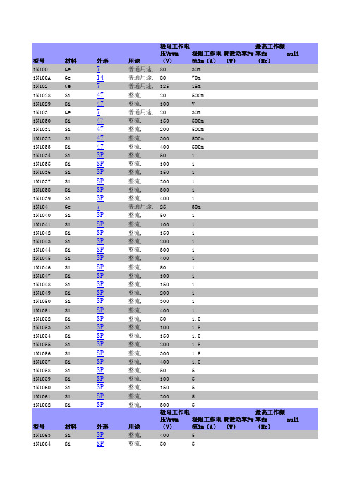
极限工作电
最高工作频
压Vrwm 极限工作电 耗散功率Pw 率fm
null
(V)
流Im(A) (W)
(Hz)
普通用途, 60
30m
普通用途, 70
20m
普通用途, 60
30m
整流,
50
35
1N1183A Si
37
1N1183R,RA Si
外形
7
3 3
1
1
整流, 整流, 整流, 整流, 整流, 普通用途, 整流, 整流, 整流, 整流, 整流, 整流, 整流, 整流, 整流, 整流, 普通用途, 整流, 整流, 整流, 整流, 整流, 整流, 整流, 整流, 整流, 整流, 整流, 整流, 整流, 整流, 整流, 整流, 整流, 整流, 整流, 整流, 整流,
400
3
快速恢复, 400
3.3
快速恢复, 400
3.3
整流,
500
3
快速恢复, 500
1
整流,
600
3
快速恢复, 600
3.3
快速恢复, 600
3.3
普通用途, 70
50m
高压,
1.5K
300m
高压,
1.5K
300m
微波,混频,
12G
极限工作电
最高工作频
压Vrwm 极限工作电 耗散功率Pw 率fm
5
1N1198 Si
SP
1N1198A Si
5
1N1199 Si
in5819中文资料_数据手册_参数
TJ = 75oC TJ = 25oC
1N5819
Reverse Voltage (Volts)
Forward Voltage (Volts)
Reverse Voltage (VR) - Volts Page 7-3
采购电子元器件上万联芯城,只售原装现货,万联芯城专 为终端客户提供电子元器件配单业务,货源均来自原厂及 代理商,客户只需访问官网,联系在线客服提交 BOM 表, 即可获得报价,为客户节省采购成本,满足客户物料需求, 点击进入万联芯城。
IN5817 20 20 20 14
IN5818 30 30 30 21
IN5819
40
Volts
40
Volts
40
Volts
28
Volts
Average Forward Rectified Current...IF(av) @ TA = 55°C
............................................. 1.0 ............................................... Amps
Typical Junction Capacitance...CJ
110
< ...................... .70 .................... > pF
Operating & Storage Temperature Range...TJ, TSTRG
....................................... -65 to 125 ............................................ °C
1N、2N、CA及ICL系列芯片资料
2N6027 2N6028 Programmable Unijunction Transistors可编程单结管
2N6426 2M6427 Darlington Transistor达林顿三极管
CA3045 CA3046 General Purpose NPN Transistor Array通用NPN三极管阵列
1N5283 1N5284 1N5285 1N5286 1N5287 1N5288 1N5289 1N5290 1N5291 1N5292 1N5293 1N5294 1N5295 1N5296 1N5297 1N5298 1N5299 1N5300 1N5301 1N5302 1N5303 1N5304 1N5305 1N5306 1N5307 1N5308 1N5309 1N5310 1N5311 1N5312 1N5313 1N5314 Current Regulator Diodes稳流二极管、稳流值0.22毫安到4.7毫安
ICL7109 12BIT Microprocessor Compatible A/D Converter 12位微处理器兼容A/D转换器
ICL7116 ICL7117 3-1/2 Digit LCD/LED display A/D Converter with Display Hold 3位半LCD/LED显示A/D转换器带显示保持。
CA3096 NPN/PNP Transistor Array NPN/PNP混合型三极管阵列
CA3304 4BIT 25MHZ Flash A/D Converter 4位25MHZ快闪A/D转换器
CA3306 6BIT 15MHZ Flash A/D Converter 6位15MHZ快闪A/D转换器
1N5819中文资料_数据手册_参数
万联芯城-电子元器件采购网,专为终端工厂 客户提供一站式电子元器件配套服务,万联芯城所售电子元器件 均为原装现货库存,提交 BOM 表立即报价。万联芯城代理长电, 顺络,先科 ST 等知名电子元器件品牌,价格有明显的优势,欢 迎广大客户咨询相关采购业务。点击进入万联芯城。
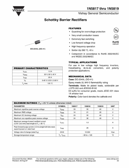
肖特基势垒整流器特征 ?保护过压保护 ?非常小的传导损失 ?极快的切换 ?低正向压降 ?高频操作 ?浸焊260°C,40秒 ?符合ROHS 2002/95 / EC的组件和WEEE 2002/96 / EC典型应用为了用于低压高频逆变器,续流,直流 - 直流转换器,和极性保护应用.机械数据案例:DO-204AL(DO-41)环氧符合UL 94V-0易燃 性等级端子:哑光镀锡导线,可焊每个 J-STD-002和JESD22-B102 E3后缀为消费级,符合JESD 201级 1A晶须测试极性:色带表示阴极端主要特征 我 (AV) 1.0 A V RRM 20 V,30 V,40 V 我 FSM 25 A V F 0.45 V,0.55 V,0.60 V T J MAX. 125°C DO-204AL(DO-41) 大额定值( 除非另有说明, T A = 25°C)参 数符号 1N5817 1N5818 1N5819单元大重复峰值反向电压 V RRM 20三十 40 V大RMS电压 V RMS 14 21 28 V大DC阻断电压 V DC 20三十 40 V大非重复峰值反向 电压 V RSM 24 36 48 V大平均正向整流电流 T L = 90°C时, 引线长度为0.375“(9.5 MM) 我 (AV) 1.0一个峰值正向浪涌电流,8.3MS单半正弦波叠加在 额定负载上 我 FSM 25一个 电压变化率(额定V R )的DV / DT 10 000 V /μS的存储温度范围 T J ,T STG - 65到+ 125 C
1N829中文资料

Philips Semiconductors
Product specification
Voltage reference diodes
PACKAGE OUTLINE
1N821 to 1N829 1N821A to 1N829A
handbook, full pagewidth
0.55 max 1.6 max 25.4 min 3.04 max 25.4 min
1996 Mar 20
2Hale Waihona Puke 元器件交易网Philips Semiconductors
Product specification
Voltage reference diodes
ELECTRICAL CHARACTERISTICS Tj = 25 °C unless otherwise specified. SYMBOL Vref ∆Vref PARAMETER reference voltage reference voltage excursion 1N821; 1N821A 1N823; 1N823A 1N825; 1N825A 1N827; 1N827A 1N829; 1N829A SZ temperature coefficient 1N821; 1N821A 1N823; 1N823A 1N825; 1N825A 1N827; 1N827A 1N829; 1N829A rdif differential resistance 1N821 to 1N829 1N821A to 1N829A Notes IZ = 7.5 mA; see Fig.4 − − IZ = 7.5 mA: see Fig.3; notes 1 and 2 CONDITIONS IZ =7.5 mA IZ =7.5 mA; test points for Tamb: −55; +25; +75; +100 °C; see Fig.2; notes 1 and 2 MIN. 5.89 − − − − − − − − − −
1N5820RLG资料
1N5820, 1N5821, 1N58221N5820 and 1N5822 are Preferred DevicesAxial Lead RectifiersThis series employs the Schottky Barrier principle in a large area metal−to−silicon power diode. State−of−the−art geometry features chrome barrier metal, epitaxial construction with oxide passivation and metal overlap contact. Ideally suited for use as rectifiers in low−voltage, high−frequency inverters, free wheeling diodes, and polarity protection diodes.Features•Extremely Low V F•Low Power Loss/High Efficiency•Low Stored Charge, Majority Carrier Conduction •Shipped in plastic bags, 500 per bag•Available in Tape and Reel, 1500 per reel, by adding a “RL’’ suffix to the part number•Pb−Free Packages are Available*Mechanical Characteristics:•Case: Epoxy, Molded•Weight: 1.1 Gram (Approximately)•Finish: All External Surfaces Corrosion Resistant and Terminal Leads are Readily Solderable•Lead Temperature for Soldering Purposes:260°C Max. for 10 Seconds•Polarity: Cathode indicated by Polarity Band*For additional information on our Pb−Free strategy and soldering details, please download the ON Semiconductor Soldering and Mounting Techniques Reference Manual, SOLDERRM/D.Preferred devices are recommended choices for future use and best overall value.MAXIMUM RATINGSRecommended Operating Conditions is not implied. Extended exposure to stresses above the Recommended Operating Conditions may affect device reliability.*THERMAL CHARACTERISTICS (Note 5)Characteristic Symbol Max Unit Thermal Resistance, Junction−to−Ambient R q JA28°C/W*ELECTRICAL CHARACTERISTICS (T L = 25°C unless otherwise noted) (Note 1)Characteristic Symbol1N58201N58211N5822UnitMaximum Instantaneous Forward Voltage (Note 2) (i F = 1.0 Amp)(i F = 3.0 Amp)(i F = 9.4 Amp)V F0.3700.4750.8500.3800.5000.9000.3900.5250.950VMaximum Instantaneous Reverse Current @ Rated dc Voltage (Note 2)T L = 25°CT L = 100°C i R2.0202.0202.020mA1.Lead Temperature reference is cathode lead 1/32″ from case.2.Pulse Test: Pulse Width = 300 m s, Duty Cycle =2.0%.*Indicates JEDEC Registered Data for 1N5820−22.ORDERING INFORMATIONDevice Package Shipping†1N5820Axial Lead500 Units/Bag500 Units/Bag1N5820G Axial Lead(Pb−Free)1N5820RL Axial Lead1500/Tape & Reel1500/Tape & Reel1N5820RLG Axial Lead(Pb−Free)1N5821Axial Lead500 Units/Bag500 Units/Bag1N5821G Axial Lead(Pb−Free)1N5821RL Axial Lead1500/Tape & Reel1500/Tape & Reel1N5821RLG Axial Lead(Pb−Free)1N5822Axial Lead500 Units/Bag500 Units/Bag1N5822G Axial Lead(Pb−Free)1N5822RL Axial Lead1500/Tape & Reel1500/Tape & Reel1N5822RLG Axial Lead(Pb−Free)†For information on tape and reel specifications, including part orientation and tape sizes, please refer to our Tape and Reel Packaging Specifications Brochure, BRD8011/D.NOTE 3 — DETERMINING MAXIMUM RATINGSReverse power dissipation and the possibility of thermal runaway must be considered when operating this rectifier at reverse voltages above 0.1 V RWM. Proper derating may be accomplished by use of equation (1).T A(max) = T J(max)* R q JA P F(A V)* R q JA P R(A V)(1) where T A(max) = Maximum allowable ambient temperature T J(max) = Maximum allowable junction temperature(125°C or the temperature at which thermalrunaway occurs, whichever is lowest) P F(A V) = Average forward power dissipationP R(A V) = Average reverse power dissipationR q JA = Junction−to−ambient thermal resistance Figures 1, 2, and 3 permit easier use of equation (1) by taking reverse power dissipation and thermal runaway into consideration. The figures solve for a reference temperature as determined by equation (2).T R = T J(max)* R q JA P R(A V)(2) Substituting equation (2) into equation (1) yields:T A(max) = T R* R q JA P F(A V)(3) Inspection of equations (2) and (3) reveals that T R is the ambient temperature at which thermal runaway occurs or where T J = 125°C, when forward power is zero. The transition from one boundary condition to the other is evident on the curves of Figures 1, 2, and 3 as a difference in the rate of change of the slope in the vicinity of 115°C. The data of Figures 1, 2, and 3 is based upon dc conditions. For use in common rectifier circuits, Table 1 indicates suggested factors for an equivalent dc voltage to use for conservative design, that is:V R(equiv) = V(FM) F(4) The factor F is derived by considering the properties of the various rectifier circuits and the reverse characteristics of Schottky diodes.EXAMPLE: Find T A(max) for 1N5821 operated in a 12−volt dc supply using a bridge circuit with capacitive filter such that I DC = 2.0 A (I F(A V) = 1.0 A), I(FM)/I(A V) = 10, Input V oltage = 10 V(rms), R q JA =40°C/W.Step 1. Find V R(equiv).Read F = 0.65 from Table 1,N V R(equiv) = (1.41) (10) (0.65) = 9.2 V. Step 2. Find T R from Figure 2. Read T R = 108°C@ V R = 9.2 V and R q JA = 40°C/W.Step 3. Find P F(A V) from Figure 6. **Read P F(A V) = 0.85 W@I(FM)I(AV)+10and I F(AV)+1.0A.Step 4. Find T A(max) from equation (3).T A(max) = 108 * (0.85) (40) = 74°C.**Values given are for the 1N5821. Power is slightly lower for the 1N5820 because of its lower forward voltage, and higher for the 1N5822. Variations will be similar for the MBR−prefix devices, using P F(A V) from Figure 6.Table 1. Values for Factor FCircuit Half Wave Full Wave, BridgeFull Wave, Center Tapped*†Load Resistive Capacitive*Resistive Capacitive Resistive Capacitive Sine Wave0.5 1.30.50.65 1.0 1.3 Square Wave0.75 1.50.750.75 1.5 1.5*Note that V R(PK)[ 2.0 V in(PK).†Use line to center tap voltage for V in.Figure 1. Maximum Reference Temperature1N5820Figure 3. Maximum Reference Temperature1N5822Figure 4. Steady−State Thermal Resistance152.0V R , REVERSE VOLTAGE (VOLTS)115125105304.0V R , REVERSE VOLTAGE (VOLTS)125115105958575L, LEAD LENGTH (INCHES)1/8252015105.002/840TR , R E F E R E N C E T E M P E R A T U R E ( C )T R J L , T H E R M A L R E S I S T A N C E9585755.03.0 4.07.01020° 5.07.01015203/84/85/86/87/81.0403530q J U N C T I O N −T O −L E A D ( C /W )°, R E F E R E N C E T E M P E R A T U R E ( C )R °115105T R , R E F E R E N C E T E M P E R A T U R E ( C )958575°125r (t ), T R A N S I E N T T H E R M A L R E S I S T A N C E (N O R M A L I Z E D )0.20.51.02.05.01020501002005001.0 k2.0 k5.0 k10 k0.050.030.020.010.1t, TIME (ms)0.50.30.21.0Figure 5. Thermal Response20 k3.00.1I F(AV), AVERAGE FORWARD CURRENT (AMP)107.05.00.70.50.1 5.0P 0.20.30.5 2.0, A V E R A G E P O W E R D I S S I P A T I O N (W A T T S )F (A V )3.02.01.00.30.20.7 1.07.010Figure 6. Forward Power Dissipation 1N5820−22NOTE 4 − APPROXIMATE THERMAL CIRCUIT MODELUse of the above model permits junction to lead thermal resistance for any mounting configuration to be found. For a given total lead length, lowest values occur when one side of the rectifier is brought as close as possible to the heat sink.Terms in the model signify:T A = Ambient Temperature T C = Case Temperature T L = Lead Temperature T J = Junction Temperature R q S = Thermal Resistance, Heatsink to Ambient R q L = Thermal Resistance, Lead−to−Heatsink R q J = Thermal Resistance, Junction−to−Case P D = Total Power Dissipation = P F + P R P F = Forward Power Dissipation P R = Reverse Power Dissipation(Subscripts (A) and (K) refer to anode and cathode sides,respectively.) Values for thermal resistance components are:R q L = 42°C/W/in typically and 48°C/W/in maximum R q J = 10°C/W typically and 16°C/W maximumThe maximum lead temperature may be found as follows:T L = T J(max) * n T JL where n T JL [ R q JL · P DNOTE 6 — HIGH FREQUENCY OPERATIONSince current flow in a Schottky rectifier is the result of majority carrier conduction, it is not subject to junction diode forward and reverse recovery transients due to minor-ity carrier injection and stored charge. Satisfactory circuit analysis work may be performed by using a model consist-ing of an ideal diode in parallel with a variable capacitance.(See Figure 10.)Figure 9. Typical Reverse Current505.0V R , REVERSE VOLTAGE (VOLTS)8.016i F , I N S T A N T A N E O U S F O R W A R D C U R R E N T (A M P )0.52432400.050.30.20.10.070.71.02.03.07.0102030V R , REVERSE VOLTAGE (VOLTS)1.00.5200702.03.05.010500300100C , C A P A C I T A N C E (p F )0.77.02030Figure 10. Typical Capacitance4.012202836PACKAGE DIMENSIONSAXIAL LEAD CASE 267−05(DO−201AD)ISSUE GNOTES:1.DIMENSIONING AND TOLERANCING PER ANSI Y14.5M, 1982.2.CONTROLLING DIMENSION: INCH.STYLE 1:PIN 1.CATHODE (POLARITY BAND)2.ANODEDIMMIN MAX MIN MAX MILLIMETERSINCHES A 0.2870.3747.309.50B 0.1890.209 4.80 5.30D 0.0470.051 1.20 1.30K1.000−−−25.40−−−ON Semiconductor and are registered trademarks of Semiconductor Components Industries, LLC (SCILLC). SCILLC reserves the right to make changes without further notice to any products herein. SCILLC makes no warranty, representation or guarantee regarding the suitability of its products for any particular purpose, nor does SCILLC assume any liability arising out of the application or use of any product or circuit, and specifically disclaims any and all liability, including without limitation special, consequential or incidental damages.“Typical” parameters which may be provided in SCILLC data sheets and/or specifications can and do vary in different applications and actual performance may vary over time. All operating parameters, including “Typicals” must be validated for each customer application by customer’s technical experts. SCILLC does not convey any license under its patent rights nor the rights of others. SCILLC products are not designed, intended, or authorized for use as components in systems intended for surgical implant into the body, or other applications intended to support or sustain life, or for any other application in which the failure of the SCILLC product could create a situation where personal injury or death may occur. Should Buyer purchase or use SCILLC products for any such unintended or unauthorized application, Buyer shall indemnify and hold SCILLC and its officers, employees, subsidiaries, affiliates,and distributors harmless against all claims, costs, damages, and expenses, and reasonable attorney fees arising out of, directly or indirectly, any claim of personal injury or death associated with such unintended or unauthorized use, even if such claim alleges that SCILLC was negligent regarding the design or manufacture of the part. SCILLC is an Equal Opportunity/Affirmative Action Employer. This literature is subject to all applicable copyright laws and is not for resale in any manner.PUBLICATION ORDERING INFORMATION。
1N5821US中文资料

矿产资源开发利用方案编写内容要求及审查大纲
矿产资源开发利用方案编写内容要求及《矿产资源开发利用方案》审查大纲一、概述
㈠矿区位置、隶属关系和企业性质。
如为改扩建矿山, 应说明矿山现状、
特点及存在的主要问题。
㈡编制依据
(1简述项目前期工作进展情况及与有关方面对项目的意向性协议情况。
(2 列出开发利用方案编制所依据的主要基础性资料的名称。
如经储量管理部门认定的矿区地质勘探报告、选矿试验报告、加工利用试验报告、工程地质初评资料、矿区水文资料和供水资料等。
对改、扩建矿山应有生产实际资料, 如矿山总平面现状图、矿床开拓系统图、采场现状图和主要采选设备清单等。
二、矿产品需求现状和预测
㈠该矿产在国内需求情况和市场供应情况
1、矿产品现状及加工利用趋向。
2、国内近、远期的需求量及主要销向预测。
㈡产品价格分析
1、国内矿产品价格现状。
2、矿产品价格稳定性及变化趋势。
三、矿产资源概况
㈠矿区总体概况
1、矿区总体规划情况。
2、矿区矿产资源概况。
3、该设计与矿区总体开发的关系。
㈡该设计项目的资源概况
1、矿床地质及构造特征。
2、矿床开采技术条件及水文地质条件。