455LP3E中文资料
CAT9555中文资料

概述CAT9555是一款基于COMS工艺的器件,它提供了I2C和SMBus在应用中的16位通用并行输入、输出口的扩展。
当应用中需要额外的I/O口来连接传感器、电源开关、LED、按钮、风扇等时,可使用I/O扩展器件实现简单的解决方案。
CAT9555包含两个8位配置寄存器(输入或输出选择)、输入寄存器、输出寄存器、极性反转寄存器和一路兼容I2C/SMBus串行接口。
通过写配置寄存器可将16个I/O口中的任何一个配置成为输入或输出。
系统主控制器可以通过写高电平有效的极性反转寄存器将CAT9555的输入数据反转。
当任何输入口状态改变时,CAT9555就会产生一个低电平中断,该中断可以用来向系统主控器指明输入端口状态的改变。
CAT9555有3个输入管脚来实现扩充I2C地址,最多允许8个器件共用在一个I2C/SMBus总线上。
CAT9555固定的I2C地址与CAT9554相同,只允许8个器件连接接到同一个I2C/SMBus总线上。
特性兼容400KHz I2C总线工作电源电压:2.3V~5.5V低待机电流I/O口可承受5V电压16个I/O口,默认为16个高电平输入口高驱动能力独立的输入输出配置寄存器极性反转寄存器低电平有效中断输出内部上电复位上电时无干扰脉冲信号SCL/SDA输入的噪声滤波器可级联8个器件工业级温度范围提供三种不同的封装形式:与RoHS兼容的24脚SOIC、TSSOP封装和24脚的TQFN封装(4mmx4mm)定制信息结构框图SOIC/TSSOP1234-111213-2021222324应用场合白色电器(洗碗机和洗衣机)手持设备(手机、PDA和数码相机)数据通信(路由器、集线器和服务器)。
LM1117_3.3中文PDF资料
电子产品。
特点
* 固定输出电压为 1.5V、1.8V、2.5V、3.3V、5.0V 和 可调版本的电压精度为 1%
* 固定电压为 1.2V 的输出电压精度为 2% * 低漏失电压:1A 输出电流时仅为 1.2V * 限流功能 * 过热切断 * 温度范围:-40°C~ 125°C
0≤IOUT≤1A, 3.2V≤VIN≤10V VOUT
X1117 -2.5,
1.764 1.800 1.836
IOUT=10mA, VIN=4.5V,TJ=25°C , 2.475 2.500 2.525 V
0≤IOUT≤1A, 3.9V≤VIN ≤10V
2.450 2.500 2.550
X1117 -3.3,
范围 20 260 150
-65 ~ +150 内部限制 (注1)
2000
单位 V °C °C °C
mW V
注1:最大允许功耗是最大工作结温TJ (max),结对空热阻θJA 和环境温度Tamb的函数。最大允许 功耗在给定的环境温度下, PD (max) = (TJ (max) - Tamb)/θJA,超过最大允许功耗会导致芯片 温度过高,调整器因此会进入到过热切断状态。不同封装类型的结对空热阻θJA 是不同的, 由封装技术决定。
应用
* 膝上型电脑,掌上电脑和笔记本 电脑
* 电池充电器 * SCSI-II主动终端 * 移动电话 * 无绳电话 * 电池供电系统 * 便携式设备 * SMPS波斯特稳压器
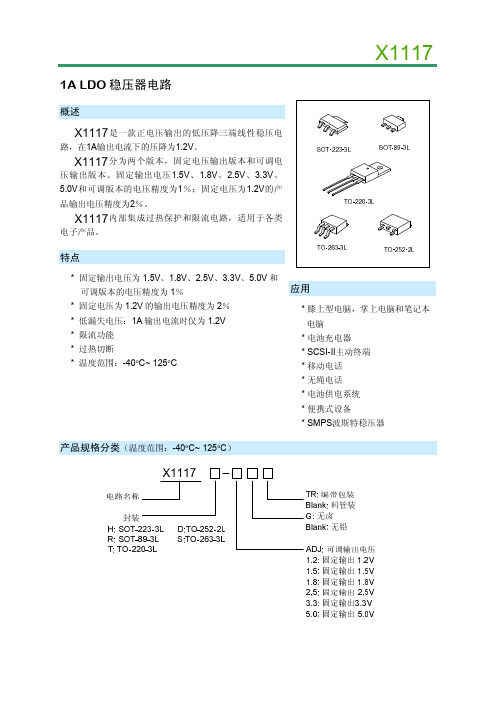
产品规格分类(温度范围:-40°C~ 125°C)
X1117
产品名称 X 1117H- ADJTR X 1117H- 1.8TR X 1117H- 3.3TR X 1117H- ADJTR X 1117H- 1.8TR X 1117H- 3.3TR
sp3232中文资料说明书

输出漏电流 低输出电压 高输出电压 驱动器输出 输出电压范围
±0.05 VCC-0.6 VCC-0.1
±10 0.4
±5.0
±5.4
输出电阻
300
输出短路电流
±35
±60
±70
±100
输出漏电流
±25
接收器输入
输入电压范围
-15
+15
输入低阈值
0.6
1.2
0.8
1.5
输入高阈值
1.5
2.4
1.8
2.4
1
RXOUT……………………………………………………………………..………………-0.3V~(VCC+0.3V) 短路期间 TXOUT……………………………………………………………………………...………………………不变 存储器温度………………………………………………………………………………………-65℃~+150℃ 每种封装的功耗 20-脚 SSOP ………………………………………………………………………………….………………………..750mW (大于+70℃时以 9.25mW/℃降低) 18-脚 PDIP ………………………………………………………………………….……………………………..1220mW (大于+70℃时以15.2mW/℃降低) 18-脚 SOIC …………………………………………………………………………….…………………………..1260mW (大于+70℃时以 15.7mW/℃降低) 20-脚 TSSOP ………………………………………………………………………………….………………………..890mW (大于+70℃时以 11.1mW/℃降低) 16-脚 SSOP ………………………………………………………………………………….………………………..775mW (大于+70℃时以 9.69mW/℃降低) 16-脚 PDIP ………………………………………………………………………………….………………………1150mW (大于+70℃时以14.3mW/℃降低) 16-脚 宽SOIC ………………………………………………………………………………….………………………..900mW (大于+70℃时以 11.2mW/℃降低) 16-脚 TSSOP ………………………………………………………………………………….………………………..850mW (大于+70℃时以 10.5mW/℃降低) 20-脚 nSOIC ………………………………………………………………………………….……………………..1086mW (大于+70℃时以 13.57mW/℃降低)
pt4115中文资料

pt4115中文资料PT4115是一款连续电感电流导通模式的降压恒流源,用于驱动一颗或多颗1W或者3W的串联LED。
1基本参数PT4115采用SOT89-5封装和ESOP8封装。
PT4115输出电流可调,最大可达1.2安培。
根据不同的输入电压和外部器件,PT4115可以驱动高达数十瓦的LED。
PT4115内置功率开关,采用高端电流采样设置LED平均电流,并通过DIM引脚可以接受模拟调光和很宽范围的PWM调光。
当DIM的电压低于0.3伏时,功率开关关断,PT4115进入极低工作电流的待机状态。
2特点1:电感越大,工作频率越低,恒流效果越好。
2:输出电流越大,需要电感值越小。
电感选择方便。
3:输出电压越高,效率越高,3 颗1W 串联比1 颗3W效率高。
4:内部含有过温保护功能,外部可设计过温保护电路,对LED有双重保护。
[1]3引脚功能①SW:功率开关的漏端。
②GND:信号和功率地。
③DIM:开关使能、模拟和PWM和调光端。
④CSN:电流采样端,采样电阻接在CSN 和VIN 端之间。
⑤VIN:电源输入端,必须就近接旁路电容。
⑥Exposed PAD:散热端,内部接地,贴在PCB 上减少热阻。
[1] 电源电压:-0.3~45V功率开关的漏端:-0.3~45V电流采样端(相对VIN):+0.3 ~(-6)VPT4115是一款工作在连续模式下的电感型降压转换器。
在电源电压高于输出电压的情况下,能高效地驱动单颗或者多颗串联LED。
IC 的输入电压范围为5V~24V,输出电流外部可调,最大输出电流可达0.7A。
PT4115内部集成功率管和高端电流检测电路,通过外部电阻可设定平均输出电流。
此外,输出电流还可以通过外部的ADJ引脚进行调整,使其低于设定值。
ADJ引脚可以接收直流电压或者PWM信号,支持线性调光或者PWM调光。
如果给ADJ引脚加一个0.2V或者更低的电压,输出功率管将会被关断,IC工作在低电流的待机模式下。
PMEG3015EV,115;中文规格书,Datasheet资料

1.Product profile1.1General descriptionPlanar Maximum Efficiency General Application (MEGA) Schottky barrier rectifier with an integrated guard ring for stress protection, encapsulated in an ultra small SMD SOT666 plastic package.1.2FeaturesForward current: 1.5 A Reverse voltage: 30 V Ultra low forward voltageUltra small SMD packages1.3ApplicationsLow voltage rectificationHigh efficiency DC-to-DC conversion Voltage clampingInverse polarity protectionLow power consumption applications1.4Quick reference data[1]Pulse test: t p ≤300μs; δ≤0.02.PMEG3015EV30 V, 1.5 A ultra low V F MEGA Schottky barrier rectifier in SOT666 packageRev. 02 — 4 February 2010Product data sheetTable 1.Quick reference data Symbol Parameter Conditions Min Typ Max Unit I F forward current T sp ≤ 55 °C-- 1.5A V R reverse voltage --30V V Fforward voltageI F =1.5A[1]-480550mV2.Pinning information3.Ordering information4.MarkingTable 2.PinningPin Description Simplified outline Symbol1cathode 2cathode 3anode 4anode 5cathode 6cathode123456sym0381,25,63, 4Table 3.Ordering informationType number Package NameDescriptionVersion PMEG3015EV-plastic surface mounted package; 6 leadsSOT666Table 4.Marking codesType number Marking code PMEG3015EV1A5.Limiting values[1]For SOT666 only valid, if pins 3 and 4 are connected in parallel.[2]Device mounted on an FR4 Printed-Circuit Board (PCB), single-sided copper, tin-plated and standard footprint.[3]Device mounted on an FR4 PCB, single-sided copper, tin-plated and mounting pad for cathode 1cm 2.6.Thermal characteristics[1]For Schottky barrier diodes thermal run-away has to be considered, as in some applications the reverse power losses P R are a significant part of the total power losses. Nomograms for determining the reverse power losses P R and I F(AV) rating will be available on request.[2]Reflow soldering is the only recommended soldering method.[3]Device mounted on an FR4 PCB, single-sided copper, tin-plated and standard footprint.[4]Device mounted on an FR4 PCB, single-sided copper, tin-plated and mounting pad for cathode 1cm 2.Table 5.Limiting valuesIn accordance with the Absolute Maximum Rating System (IEC 60134).Symbol Parameter Conditions Min Max Unit V R reverse voltage -30V I F forward currentT sp ≤ 55 °C- 1.5A I FRM repetitive peak forward current t p ≤1ms; δ≤0.25[1]- 4.5A I FSM non-repetitive peak forward currentt p =8ms; square wave [1]-9.5A P tot total power dissipation T amb ≤ 25 °C[2]-0.31W [3]-0.58W T j junction temperature -150°C T amb ambient temperature −65+150°C T stgstorage temperature−65+150°CTable 6.Thermal characteristics Symbol ParameterConditionsMin Typ Max Unit R th(j-a)thermal resistance from junction to ambientin free air [1][2][3]--405K/W [4]--215K/W R th(j-sp)thermal resistance from junction to solder point--80K/W7.CharacteristicsTable 7.CharacteristicsT amb=25°C unless otherwise specified.Symbol Parameter Conditions Min Typ Max UnitV F forward voltage I F=1 mA[1]-125160mVI F=10mA[1]-185220mVI F=100 mA[1]-255290mVI F=500 mA[1]-340380mVI F=1 A[1]-410480mVI F=1.5 A[1]-480550mVI R reverse current V R=10V-60150μAV R=30V-4001000μAC d diode capacitance V R=1V;f=1MHz-6072pF[1]Pulse test: t p≤300μs; δ≤0.02.8.Package outline9.Packing informationTable 8.Packing methodsThe indicated -xxx are the last three digits of the 12NC ordering code.[1]Type number Package Description Packing quantity4000PMEG3015EV SOT666 4 mm pitch, 8 mm tape and reel-115[1]For further information and the availability of packing methods, see Section13.10.Soldering11.Revision historyTable 9.Revision historyDocument ID Release date Data sheet status Change notice SupersedesPMEG3015EV_220100204Product data sheet-PMEG3015EV_1 Modifications:•This data sheet was changed to reflect the new company name NXP Semiconductors,including new legal definitions and disclaimers. No changes were made to the technicalcontent.PMEG3015EV_120050404Product data sheet--12.Legal information12.1Data sheet status[1]Please consult the most recently issued document before initiating or completing a design. [2]The term ‘short data sheet’ is explained in section “Definitions”.[3]The product status of device(s) described in this document may have changed since this document was published and may differ in case of multiple devices. The latest product status information is available on the Internet at URL .12.2DefinitionsDraft — The document is a draft version only. The content is still under internal review and subject to formal approval, which may result in modifications or additions. NXP Semiconductors does not give any representations or warranties as to the accuracy or completeness ofinformation included herein and shall have no liability for the consequences of use of such information.Short data sheet — A short data sheet is an extract from a full data sheet with the same product type number(s) and title. A short data sheet is intended for quick reference only and should not be relied upon to contain detailed and full information. For detailed and full information see the relevant full data sheet, which is available on request via the local NXP Semiconductors sales office. In case of any inconsistency or conflict with the short data sheet, the full data sheet shall prevail.12.3DisclaimersGeneral — Information in this document is believed to be accurate andreliable. However, NXP Semiconductors does not give any representations or warranties, expressed or implied, as to the accuracy or completeness of such information and shall have no liability for the consequences of use of such information.Right to make changes — NXP Semiconductors reserves the right to make changes to information published in this document, including withoutlimitation specifications and product descriptions, at any time and without notice. This document supersedes and replaces all information supplied prior to the publication hereof.Suitability for use — NXP Semiconductors products are not designed, authorized or warranted to be suitable for use in medical, military, aircraft, space or life support equipment, nor in applications where failure ormalfunction of an NXP Semiconductors product can reasonably be expected to result in personal injury, death or severe property or environmentaldamage. NXP Semiconductors accepts no liability for inclusion and/or use of NXP Semiconductors products in such equipment or applications and therefore such inclusion and/or use is at the customer’s own risk.Applications — Applications that are described herein for any of these products are for illustrative purposes only. NXP Semiconductors makes no representation or warranty that such applications will be suitable for the specified use without further testing or modification.Limiting values — Stress above one or more limiting values (as defined in the Absolute Maximum Ratings System of IEC 60134) may cause permanent damage to the device. Limiting values are stress ratings only and operation of the device at these or any other conditions above those given in theCharacteristics sections of this document is not implied. Exposure to limiting values for extended periods may affect device reliability.Terms and conditions of sale — NXP Semiconductors products are sold subject to the general terms and conditions of commercial sale, as published at /profile/terms , including those pertaining to warranty, intellectual property rights infringement and limitation of liability, unlessexplicitly otherwise agreed to in writing by NXP Semiconductors. In case of any inconsistency or conflict between information in this document and such terms and conditions, the latter will prevail.No offer to sell or license — Nothing in this document may be interpreted or construed as an offer to sell products that is open for acceptance or the grant, conveyance or implication of any license under any copyrights, patents or other industrial or intellectual property rights.Export control — This document as well as the item(s) described herein may be subject to export control regulations. Export might require a prior authorization from national authorities.Quick reference data — The Quick reference data is an extract of theproduct data given in the Limiting values and Characteristics sections of this document, and as such is not complete, exhaustive or legally binding.12.4TrademarksNotice: All referenced brands, product names, service names and trademarks are the property of their respective owners.13.Contact informationFor more information, please visit: For sales office addresses, please send an email to: salesaddresses@Document status [1][2]Product status [3]DefinitionObjective [short] data sheet Development This document contains data from the objective specification for product development. Preliminary [short] data sheet Qualification This document contains data from the preliminary specification. Product [short] data sheetProductionThis document contains the product specification.14.Contents1Product profile. . . . . . . . . . . . . . . . . . . . . . . . . . 11.1General description . . . . . . . . . . . . . . . . . . . . . 11.2Features. . . . . . . . . . . . . . . . . . . . . . . . . . . . . . 11.3Applications . . . . . . . . . . . . . . . . . . . . . . . . . . . 11.4Quick reference data . . . . . . . . . . . . . . . . . . . . 12Pinning information. . . . . . . . . . . . . . . . . . . . . . 23Ordering information. . . . . . . . . . . . . . . . . . . . . 24Marking. . . . . . . . . . . . . . . . . . . . . . . . . . . . . . . . 25Limiting values. . . . . . . . . . . . . . . . . . . . . . . . . . 36Thermal characteristics . . . . . . . . . . . . . . . . . . 37Characteristics. . . . . . . . . . . . . . . . . . . . . . . . . . 48Package outline. . . . . . . . . . . . . . . . . . . . . . . . . 69Packing information . . . . . . . . . . . . . . . . . . . . . 610Soldering . . . . . . . . . . . . . . . . . . . . . . . . . . . . . . 711Revision history. . . . . . . . . . . . . . . . . . . . . . . . . 812Legal information. . . . . . . . . . . . . . . . . . . . . . . . 912.1Data sheet status . . . . . . . . . . . . . . . . . . . . . . . 912.2Definitions. . . . . . . . . . . . . . . . . . . . . . . . . . . . . 912.3Disclaimers. . . . . . . . . . . . . . . . . . . . . . . . . . . . 912.4Trademarks. . . . . . . . . . . . . . . . . . . . . . . . . . . . 913Contact information. . . . . . . . . . . . . . . . . . . . . . 914Contents. . . . . . . . . . . . . . . . . . . . . . . . . . . . . . 10Please be aware that important notices concerning this document and the product(s)described herein, have been included in section ‘Legal information’.© NXP B.V.2010.All rights reserved.For more information, please visit: For sales office addresses, please send an email to: salesaddresses@分销商库存信息: NXPPMEG3015EV,115。
sp3232中文资料说明书
注释 1:V+和 V-幅值最大可达 7V,但他们的绝对差值不能超过 13V。
参数规范
除 非 特 别 规 定 , 以 下 规 范 适 用 于 Vcc = +3.0V~5.0V ; TAMB=TMIN~TMAX 。 典 型 值 的 适 用 条 件 :
VCC=+3.3V~5.0V 和 TAMB=25℃。
参数
图 5 SP3222E 管脚配置
VCC
+ C5 0.1u F
19 VCC
u
2 C1+ +
3
V+
+
C1 0.1u F
*C3 0.1u F
u
u
4 C1-
5 C2+
V- 7
+
C2 0.1 u F 6 C2-
C4 0.1 u F
u
+
u
13 T1IN 12 T2IN
T1OUT 17 T2OUT 8
RS-232
ns
ns
|tPHL-tPLH|, TAMB=25℃
ns
|tPHL-tPLH|
3
续上表 参数
转换区中的电压 变化速度
最小
典型
最大 30
单位 V/µS
条件 VCC=3.3V,RL=3KΩ,TAMB=25 ℃ , 测 量 范 围 -3.0V~+3.0V 或 +3.0V~-3.0V
注释 2:驱动器输入滞后典型值为 250mV。
VCC=5.0V, 注释 2
µA
TXIN, EN , SHDN ,
TAMB=+25℃
µA
接收器禁用
V
IOUT=1.6mA
美国Lighthouse(莱特浩斯)P3和P5尘埃粒子计数器中文资料

P3/P5便携式尘埃粒子计数器Apex便携式尘埃粒子计数器可4通道同时检测,最多可达到50个预设检测方案以及多达3000组数据存储空间。
数据可以通过U盘、电脑、监控系统和自建自动化系统Apex尘埃粒子计数器的数据可通过RS485通讯协议和以太网接口进行数据通讯。
特征·0.3-10μm范围检测·28.3L/min采样流速·3.5英寸彩色触摸屏操作·3000组数据存储·仪器自行故障诊断·网页浏览Apex便携式尘埃粒子计数器特征P3P5最小检测粒径0.3μm0.5μm标准两通道0.3,0.5,μm0.5,5.0μm可选四通道0.3,0.5,1.0,5.0μm0.5,1.0,5.0,10.0μm可更改粒径通道0.3,0.5,0.7,1.0,3.0,5.0μm0.5,0.7,1.0,3.0,5.0,7.0,10.0μm技术资料流速 1.0立方英尺(28.3L/min)通讯以太网通讯协议TCP、RTU、ASCII端口以太网、RS485(RJ45)、USB屏幕 3.5英寸彩色触摸屏数据存储3000组区域标示200个自行诊断是网页浏览是音频报警是内建报告ISO14644-1、EU-GMP Annex1、FS-209E数据存储安全设计符合21CFR Part11语言英语、西班牙语、德语、法语、意大利语、俄语、简体中文、日语、韩语尺寸9.00×6.21×8.46″(22.8×15.8×21.5cm)重量10镑(4.5Kg)材质304不锈钢电源24VDC电池正常4小时;持续采样3小时真空源内置真空泵,自动流速控制采样输出过滤内置HEPA高效过滤器(>99.97%@0.3μm)采样模式自动、手动、蜂鸣、浓度校准依据ISO21501-4自净时间<1/5分钟per ISO21501-4浓度限制500,000/立方英尺(17,150,000/m3)@5%重叠损失从ISO classes 1-8洁净室计数效能50%@最小粒径通道;100%for particles>1.5X-2X第一个通道选项软件LMS Express,LMS Express RT,LMS Pharma打印机USB打印机。
AK5355VTP-E2;中文规格书,Datasheet资料

SEL
DIF
LIN RIN
VCOM VA VSS
ADC
HPF
Audio I/F Controller
Clock Divider
LRCK BCLK SDTO
VD
PDN
MCLK
MS0113-E-01 -1-
/
NC
16
TST1 17
NC
18
NC
19
VCOM 20
AK5355
Top View
10 SDTO 9 NC 8 NC 7 NC 6 SEL
5
4
VSS 3
2
RIN 1
VD
VA
LI N
MS0113-E-01 -2-
/
2005/01
ASAHI KASEI
PIN/FUNCTION (AK5355VT)
Ta
-40
Storage Temperature
Tstg
-65
Note 1. All voltages with respect to ground.
max 4.6 4.6 ±10 VA+0.3 VD+0.3 85 150
WARNING: Operation at or beyond these limits may results in permanent damage to the device. Normal operation is not guaranteed at these extremes.
7 NC
-
NC Pin (No internal bonding) This pin should be left floating.