JAN5819UR-1中文资料
1N5519B中文资料

B-C-D SUFFIX MAX. NOISE DENSITY @1Z=250µ A ND
REGULATION FACTOR ∆VZ (NOTE 5) VOLTS
LOW VZ CURRENT 1ZL
mAdc
µ Adc
5.0 3.0 1.0 3.0 2.0 2.0 2.0 1.0 1.0 0.5 0.5 0.1 0.05 0.05 0.05 0.01 0.01 0.01 0.01 0.01 0.01 0.01 0.01 0.01 0.01 0.01 0.01 0.01 0.01
NOTE 2 NOTE 3 NOTE 4 NOTE 5
Reverse leakage currents are measured at VR as shown on the table. ∆VZ is the maximum difference between VZ at lZT and VZ at lZL measured with the device junction in thermal equilibrium at the ambient temperature of +25°C +3°C.
Junction and Storage Temperature: -65°C to +175°C DC Power Dissipation: 500 mW @ +50°C Power Derating: 4 mW / °C above +50°C Forward Voltage @ 200mA: 1.1 volts maximum ELECTRICAL CHARACTERISTICS @ 25°C
26 24 22 18 22 26 30 30 30 35 40 45 60 80 90 90 100 100 100 100 100 100 100 100 100 100 100 100 100
MIL-STD-1916介绍 Auras
III
IV
2000
5000
32
125
0,1
1,2
50
125
1,2
3,4
64
80
32
32
p 12
MIL-STD-1916 抽樣標準中之結語
in5819中文资料_数据手册_参数
TJ = 75oC TJ = 25oC
1N5819
Reverse Voltage (Volts)
Forward Voltage (Volts)
Reverse Voltage (VR) - Volts Page 7-3
采购电子元器件上万联芯城,只售原装现货,万联芯城专 为终端客户提供电子元器件配单业务,货源均来自原厂及 代理商,客户只需访问官网,联系在线客服提交 BOM 表, 即可获得报价,为客户节省采购成本,满足客户物料需求, 点击进入万联芯城。
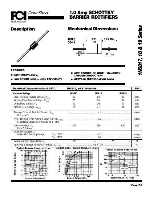
IN5817 20 20 20 14
IN5818 30 30 30 21
IN5819
40
Volts
40
Volts
40
Volts
28
Volts
Average Forward Rectified Current...IF(av) @ TA = 55°C
............................................. 1.0 ............................................... Amps
Typical Junction Capacitance...CJ
110
< ...................... .70 .................... > pF
Operating & Storage Temperature Range...TJ, TSTRG
....................................... -65 to 125 ............................................ °C
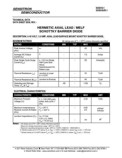
SS5819-1中文资料
STYLE
φB
φD
G
L
.028/.034 .08/.107 .160/.205 1.00/1.30
DO-41
0.71/0.86 2.03/2.72 4.06/5.21 25.4/33.02
SCHOTTKY BARRIER
1N5819UR-1
PACKAGE DIMENSIONS - INCHES ( MILLIMETERS)
UNIT Volts
µAmps mAmps
pF
• 221 West Industry Court Deer Park, NY 11729-4681 Phone (631) 586 7600 Fax (631) 242 9798 • • World Wide Web - • E-mail Address - sales@ •
MAXIMUM RATINGS RATING
CONDITIONS
All ratings are at TA = 25oC unless otherwise specified.
MIN
TYP
MAX
UNIT
Peak Inverse Voltage
←
(PIV)
-
-
45
Vdc
Average DC Output
100 125 °C
10-1
10-2
100 °C 25 °C
10-3 0.0 0.1 0.2 0.3 0.4 0.5 0.6 Forward Voltage Drop - V F (V)
Junction Capacitance - C T (pF)
Instantaneous Reverse Current - I R (mA)
S5819中文资料

0.60 0.90
Volts mA
o
C/W pF
o
C C
o
NOTES: 1. Measured at 1MHz and applied reverse voltage of 4.0V D.C. 2. Thermal Resistance Junction to Ambient
1
E-mail: sales@ Web Site:
Symbols Maximum Repetitive Peak Reverse Voltage Maximum RMS Voltage Maximum DC Blocking Voltage Maximum Average Forward Rectified Current at TL=110℃ Peak Forward Surge Current 8.3ms single half sinewave superimposed on rated load (JEDEC Method) Maximum Forward Voltage at 1.0A D.C. Maximum Forward Voltage at 3.0A D.C. Maximum DC Reverse Current(Note l) at Rated DC blocking voltage Maximum Thermal Resistance (Note 1) Typical Junction Capacitance(Note 2) Operating Junction Temperature Range Storage termperature range TA=25 C TA=125 C
元器件交易网
MASTER INSTRUMENT CORPORATION
SAE J581-1998
SAE Technical Standards Board Rules provide that: “This report is published by SAE to advance the state of technical and engineering sciences. The use of this report is entirely voluntary, and its applicability and suitability for any particular use, including any patent infringement arising therefrom, is the sole responsibility of the user.”SAE reviews each technical report at least every five years at which time it may be reaffirmed, revised, or cancelled. SAE invites your written comments and suggestions.QUESTIONS REGARDING THIS DOCUMENT: (724) 772-8512 FAX: (724) 776-0243TO PLACE A DOCUMENT ORDER; (724) 776-4970 FAX: (724) 776-0790SAE WEB ADDRESS 5.Tests5.1SAE J575—The following test procedures in SAE J575 are a part of this report with the modifications indi-cated:5.1.1V IBRATION T EST5.1.2M OISTURE T EST5.1.3D UST T EST—(Dust test shall not be required for sealed units.)5.1.4C ORROSION T EST5.1.5W ARPAGE T EST—(Devices produced from plastic components.)5.1.6 A P HOTOMETRIC T EST5.1.6.1The photometric tests for bulb replaceable units shall be made at a distance of at least 18.3 m (60 ft) fromthe photometer to the lamp.5.1.6.2Lamp Aim—A lamp or sealed beam unit, which is designed to be aimed mechanically, shall be centered onthe photometric axis with the aiming planes normal to that axis. A lamp or sealed unit, not designed to be aimed mechanically, shall be photoelectrically aimed so that the test points in Figure 1 designated by the squares have equal intensity and those designated by triangles have equal intensity.FIGURE 1—TEST POINTS ON A SCREEN A T 7.6 m5.2Color Test—SAE J578 is a part of this report.6.Requirements6.1Performance Requirements6.1.1SAE J575—A device when tested in accordance with the test procedures in Section 5, shall meet the following requirements in SAE J575, with the modifications indicated:6.1.1.1Vibration 6.1.1.2Moisture 6.1.1.3Dust 6.1.1.4Corrosion6.1.1.5Warpage Test on Devices with Plastic Components6.1.1.6Photometry—The lamp under test shall meet the photometric requirements contained in Table 1.6.2Color—The color of the emitted light shall be white as defined in SAE J578.6.3Plastic Materials—The plastic materials used in optical parts shall meet the requirements in SAE J576.7.Guidelines7.1The photometric design guidelines for auxiliary driving lamps, when tested in accordance with 5.1.6 of this document, are contained in T able 2.TABLE 1—PHOTOMETRIC REQUIREMENTSTest Point Degrees (1)1. A tolerance of ±1/4 degree in location may be allowed atany test point.Candela, cd2U—3R and 3L 1600 min 1U—3R and 3L4000 minH—V 20 000 min and 60 000 maxH—3R and 3L 8000 min 1D—6R and 6L 2960 min 2D—6R and 6L1600 min 4D—V6000 maxTABLE 2—PHOTOMETRIC DESIGN GUIDELINESTest Point Degrees (1)1. A tolerance of ±1/4 degree in location may be allowed atany test point.Candela, cd2U—3R and 3L 2000 min 1U—3R and 3L5000 minH—V 25 000 min and 50 000 maxH—3R and 3L 10 000 min 1D—6R and 6L 3700 min 2D—6R and 6L2000 min 4D V5000 max7.2These guidelines apply to the device as used on the vehicle and are not a part of the laboratory testprocedures and requirements.7.3Lamp Aim—The lamp aim adjustments on the vehicle should be with mechanical aimers, if possible. Set themechanical aim to 0-0, reference SAE J599.7.4Other Aiming Procedures—If the vehicle mounting or lamp design precludes mechanical aiming, the lampshall be aimed photometrically (see 5.1.6.2), or visually aimed. The correct visual aim is with the high intensity zone of the beam symmetric about and 38 mm (1.5 in) below the H-V axis of the lamp on an aiming screen at7.6 m (25 ft).8.Notes8.1Marginal Indicia—The change bar (l) located in the left margin is for the convenience of the user in locatingareas where technical revisions have been made to the previous issue of the report. An (R) symbol to the left of the document title indicates a complete revision of the report.PREPARED BY THE SAE ROAD ILLUMINA TION DEVICES STANDARDS COMMITTEERationale—The Title on this document has changed. This Document has changed to comply with the new SAE Technical Standards Board format. Definitions have changed to Section 3. All other Section numbers have changed.Relationship of SAE Standard to ISO Standard—Not applicable.Application—This SAE Standard provides test procedures, performance requirements, and guidelines for auxiliary driving lamps.Reference SectionSAE J575—Tests for Motor Vehicle Lighting Devices and ComponentsSAE J576—Plastic Materials for Use in Optical Parts Such as Lenses and Reflectors of Motor Vehicle Lighting DevicesSAE J578—Color SpecificationSAE J599—Lighting Inspection CodeSAE J759—Lighting Identification CodeDeveloped by the SAE Road Illumination Devices Standards Committee。
DL5819中文资料

Maximum Ratings
• • • Operating Temperature: -55°C to +125°C Storage Temperature: -55°C to +150°C Maximum Thermal Resistance; 15 °C/W Junction To Lead MCC Catalog Number Device Marking Maximum Recurrent Peak Reverse Voltage 20V 30V 40V Maximum RMS Voltage Maximum DC Blocking Voltage
C
B
A
DL5817 DL5818 DL5819
-------
14V 21V 28V
20V 30V 40V
DIMENSIONS INCHES MIN .190 --.095 MM MIN 4.80 --2.40
Electrical Characteristics @ 25°C Unless Otherwise Specified
Figure 3 Typical Reverse Characteristics 100 10 125°C mA 1 .1 75°C .01 25°C .001 0 4 8 12 16 20 Volts Typical Reverse Current - mAversus Reverse Voltage - Volts 24 28 32 36 40 5818 5819
Figure 3 Typical Reverse Characteristics 100 10 1 .1 .01 .001 0 25°C 125°C
mA
75°C
5
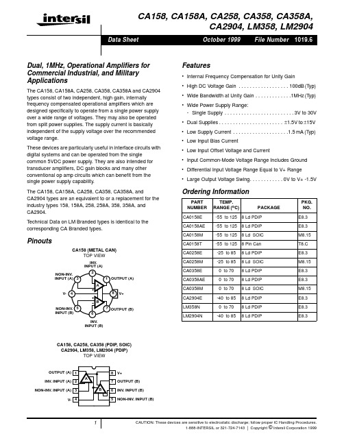
CA0158E中文资料
1. This input current will only exist when the voltage at any of the input leads is driven negative. This current is due to the collector base junction of the input PNP transistors becoming forward biased and thereby acting as input diode clamps. In addition to this diode action, there is also lateral NPN parasitic transistor action on the IC chip. This transistor action can cause the output voltages of the amplifiers to go to the V+ voltage level (or to ground for a large overdrive) for the time duration that an input is driven negative. This transistor action is not destructive and normal output states will re-establish when the input voltage, which was negative, again returns to a value greater than -0.3V.
Maximum Storage Temperature Range . . . . . . . . . . -65oC to 150oC
- 1、下载文档前请自行甄别文档内容的完整性,平台不提供额外的编辑、内容补充、找答案等附加服务。
- 2、"仅部分预览"的文档,不可在线预览部分如存在完整性等问题,可反馈申请退款(可完整预览的文档不适用该条件!)。
- 3、如文档侵犯您的权益,请联系客服反馈,我们会尽快为您处理(人工客服工作时间:9:00-18:30)。
MAXIMUM REVERSE LEAKAGE CURRENT AT RATED VOLTAGE IR @ +25°C mA 0.1 0.1 0.1 0.05 0.1 0.1 0.1 0.10 0.1 0.1 0.1 0.1 0.1 0.1 0.1 IR @ +100°C mA 5.0 5.0 5.0 5.0 6.0 6.0 6.0 12.0 5.0 5.0 5.0 5.0 12.0 12.0 12.0
CDLL5817
IR, REVERSE CURRENT (mA)
1.0
CDLL5819
0.1
CDLL5818 CDLL5817
0.01
0.001 +25 +50 +75 +100 +125
TJ , JUNCTION TEMPERATURE (°C)
FIGURE 1
TYPICAL FORWARD VOLTAGE 100.0 IF, FORWARD CURRENT, INSTANTANEOUS (AMPS)
元器件交易网
• 1N5819UR-1 AND 1N6761UR-1 AVAILABLE IN AND JANS PER MIL-PRF-19500/586 • 1 AMP SCHOTTKY BARRIER RECTIFIERS • HERMETICALLY SEALED • LEADLESS PACKAGE FOR SURFACE MOUNT • METALLURGICALLY BONDED
20 30 40 45 60 80 100 100 20 30 40 50 60 80 100
6 LAKE STREET, LAWRENCE, MASSACHUSETTS 01841 PHONE (978) 620-2600 FAX (978) 689-0803 WEBSITE:
CDI TYPE NUMBER
Байду номын сангаас
WORKING PEAK REVERSE VOLTAGE VRWM VOLTS
MAXIMUM FORWARD VOLTAGE VF @ 0.1A VOLTS 0.36 0.36 0.36 0.34 0.38 0.38 0.38 0.38 0.36 0.36 0.36 0.36 0.38 0.38 0.38 VF @ 1.0A VOLTS 0.60 0.60 0.60 0.49 0.69 0.69 0.69 0.69 0.60 0.60 0.60 0.60 0.69 0.69 0.69 VF @ 3.1A VOLTS 0.9 0.9 0.9 0.8 N/A N/A N/A N/A 0.9 0.9 0.9 0.9 N/A N/A N/A
10.0
1.0
0.1
0.01 0.1 0.2 0.3 0.4 0.5 0.6 0.7 0.8 0.9 1.0 1.1
VF, FORWARD VOLTAGE, INSTANTANEOUS (VOLTS)
148
FIGURE 2
ELECTRICAL CHARACTERISTICS @ 25°C, unless otherwise specified.
DIM D F G G1 S
MILLIMETERS MIN MAX 2.39 2.66 0.41 0.55 4.80 5.20 4.11 REF. 0.03 MIN.
INCHES MIN MAX .094 .105 .016 .022 .189 .205 .159 REF. .001 MIN.
147
元器件交易网
thru CDLL5819 and CDLL6759 thru CDLL6761 and CDLL1A20 thru CDLL1A100
TYPICAL REVERSE LEAKAGE CURRENT AT RATED PIV (PULSED) 10.0
JAN, JANTX, JANTXV
1N5819UR and CDLL5817 thru CDLL5819 and CDLL6759 thru CDLL6761 and CDLL1A20 thru CDLL1A100
MAXIMUM RATINGS
Operating Temperature: -55°C to +125°C Storage Temperature: -55°C to +150°C Average Rectified Forward Current: 1.0 AMP @TEC = +55°C Derating: 14 mA / °C above TEC = +55°C
FIGURE 1
DESIGN DATA
CASE: DO-213AB, Hermetically sealed glass case. (MELF, LL41) LEAD FINISH: Tin / Lead THERMAL RESISTANCE: (ROJEC): 40 ÞC/W maximum at L = 0 inch THERMAL IMPEDANCE: (ZOJX): 12 ÞC/W maximum POLARITY: Cathode end is banded. MOUNTING SURFACE SELECTION: The Axial Coefficient of Expansion (COE) Of this Device is Approximately +6PPM/°C. The COE of the Mounting Surface System Should Be Selected To Provide A Suitable Match With This Device.
CDLL5817 CDLL5818 CDLL5819 J,JX,JV & JS 5819UR-1 CDLL6759 CDLL6760 CDLL6761 J,JX,JV & JS 6761UR-1 CDLL1A20 CDLL1A30 CDLL1A40 CDLL1A50 CDLL1A60 CDLL1A80 CDLL1A100