MAX4820EUP中文资料
MAX485ECPA中文资料
MAX481E/MAX483E/MAX485E/MAX487E–MAX491E/MAX1487E
19-0410; Rev 3; 7/96
±15kV ESD-Protected, Slew-Rate-Limited, Low-Power, RS-485/RS-422 Transceivers
±15kV ESD-Protected, Slew-Rate-Limited, Low-Power, RS-485/RS-422 Transceivers
ABSOLUTE MAXIMUM RATINGS
Supply Control
Voltage (VCC) Input Voltage
.(.–R—..E.–..,..D..E..)........................................-.0....5..V...t.o...(.V..C...C...+...0...152VV)
Drivers are short-circuit current limited, and are protected against excessive power dissipation by thermal shutdown circuitry that places their outputs into a high-impedance state. The receiver input has a fail-safe feature that guarantees a logic-high output if the input is open circuit.
14-Pin Plastic DIP (derate 10.00mW/°C above +70°C) ..800mW 8-Pin SO (derate 5.88mW/°C above +70°C).................471mW 14-Pin SO (derate 8.33mW/°C above +70°C)...............667mW Operating Temperature Ranges MAX4_ _C_ _/MAX1487EC_ A .............................0°C to +70°C MAX4_ _E_ _/MAX1487EE_ A...........................-40°C to +85°C Storage Temperature Range .............................-65°C to +160°C Lead Temperature (soldering, 10sec) .............................+300°C
沛城4820通信铁锂BMS规格书P16S20A-4435-29

BMS产品规格书目录1. 简介 (5)2. 功能特性 (5)3. 功能示意框图 (6)4. 电气特性 (6)4.1 基本参数设置 (6)4.2 LED指示说明 (8)4.3 蜂鸣器动作说明 (9)4.4 按键说明 (9)4.5 休眠及唤醒 (9)5 通信说明 (10)5.1 RS232通信 (10)5.2 RS485通信 (10)5.3 拨码开关设置 (10)6 接口定义 (11)6.1 接口图示 (11)6.2 电气接口定义 (12)6.3 安装连接说明 (13)7 实物图和尺寸图 (13)8 使用注意事项 (14)1.简介随着锂电池在通信行业的广泛应用,对电池管理系统也提出了高性能、高可靠性及高性价比等要求。
本产品是专门针对基站后备电池设计的BMS,采用集成化的设计将采集、管理、通信等功能集成于一体。
可广泛应用在室内室外基站,如一体化基站、边际站、直放站、宏基站、太阳能基站等。
2.功能特性●具有单体电压、总体电压检测,过充、过放告警及保护功能。
常温下静态电压采样精度可达≤20mV。
●具有充、放电电流检测,充、放电过流告警及保护功能。
充电电流显示为正,放电电流显示为负,常温下电流采样精度可达≤2%@FS。
●具有电芯温度检测,电芯高、低温告警及保护功能,常温下温度采样精度可达≤3℃。
●短路保护功能。
●具有充电均衡功能。
●电芯容量估算功能。
电池组满充容量、当前容量、设计容量可以通过上位机进行设置,在进行完整充放电循环后容量可自动更新。
●LED状态指示功能。
●上位机软件控制功能,可通过上位机软件方便地对过充、过放、充放电过流、过温、欠温等保护参数,容量、休眠、均衡等参数进行设置。
●RS232通信功能,采用隔离通信。
●RS485通信功能,采用隔离通信。
3. 功能示意框图4. 电气特性4.1基本参数设置 (注:以下参数除特殊注明以外,25℃环温下测试)指示说明表1 LED工作状态指示表2 容量指示说明表3 LED闪动说明备注:可通过上位机使能或禁止LED指示灯告警,出厂默认为使能的。
MAX4203EUA+,MAX4203ESA+,MAX4205EUA+,MAX4204ESA+,MAX4201ESA+T, 规格书,Datasheet 资料

MAX4200–MAX4205
Ultra-High-Speed, Low-Noise, Low-Power, SOT23 Open-Loop Buffers
ABSOLUTE MAXIMUM RATINGS
Supply Voltage (VCC to VEE)................................................+12V Voltage on Any Pin to GND..............(VEE - 0.3V) to (VCC + 0.3V) Output Short-Circuit Duration to GND........................Continuous Continuous Power Dissipation (TA = +70°C)
MAX4203/MAX4204/MAX4205
IB RIN AV PSR ROUT
IOUT
ISC
VOUT
(Note 1)
-3.0V ≤ VOUT ≤ 3.0V
MAX4200/MAX4203, REXT = 150Ω MAX4201/MAX4204, REXT = 50Ω MAX4202/MAX4205, REXT = 75Ω
19-1338; Rev 3; 3/07
MAX4200–MAX4205
Ultra-High-Speed, Low-Noise, Low-Power, SOT23 Open-Loop Buffers
________________General Description
The MAX4200–MAX4205 are ultra-high-speed, openloop buffers featuring high slew rate, high output current, low noise, and excellent capacitive-load-driving capability. The MAX4200/MAX4201/MAX4202 are single buffers, while the MAX4203/MAX4204/MAX4205 are dual buffers. The MAX4201/MAX4204 have integrated 50Ω termination resistors, making them ideal for driving 50Ω transmission lines. The MAX4202/MAX4205 include 75Ω back-termination resistors for driving 75Ω transmission lines. The MAX4200/MAX4203 have no internal termination resistors.
MAX479中文资料

19-0127; Rev. 1; 11/98
17µA Max, Dual/Quad, Single-Supply, Precision Op Amps
_______________General Description
The MAX478 and MAX479 are dual and quad micropower, precision op amps available in 8-pin and 14-pin DIP and small-outline packages, respectively. Both devices feature an extremely low, 17µA max supply current per op amp, 70µV max offset voltage, 2.2µV/°C max offset voltage drift (0.5µV/°C typ), and 250pA max input offset current. The MAX478 and MAX479 operate from a single supply. The input voltage range includes ground, and the output swings to within a few millivolts of ground, which eliminates pull-down resistors and saves power. Both devices are optimized for single 3V and 5V supply operation, with guaranteed specifications at each supply voltage. Specifications for ±15V operation are also provided.
MEMORY存储芯片MAX490CPA+中文规格书
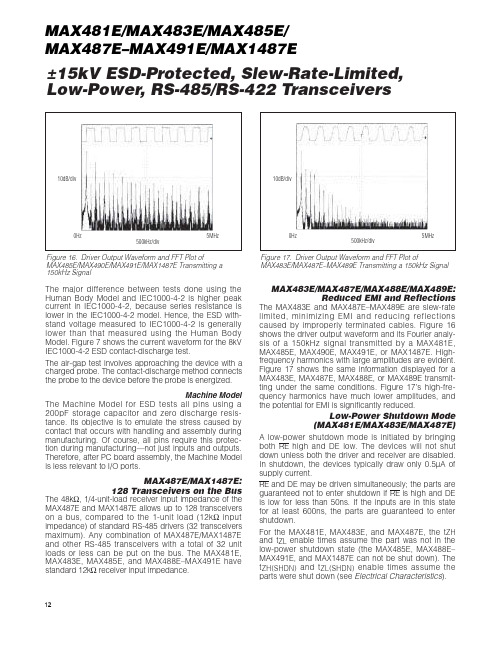
±15kV ESD-Protected, Slew-Rate-Limited, Low-Power, RS-485/RS-422 TransceiversThe major difference between tests done using the Human Body Model and IEC1000-4-2 is higher peak current in IEC1000-4-2, because series resistance is lower in the IEC1000-4-2 model. Hence, the ESD with-stand voltage measured to IEC1000-4-2 is generally lower than that measured using the Human Body Model. Figure 7 shows the current waveform for the 8kV IEC1000-4-2 ESD contact-discharge test.The air-gap test involves approaching the device with a charged probe. The contact-discharge method connects the probe to the device before the probe is energized.Machine Model The Machine Model for ESD tests all pins using a 200pF storage capacitor and zero discharge resis-tance. Its objective is to emulate the stress caused by contact that occurs with handling and assembly during manufacturing. Of course, all pins require this protec-tion during manufacturing—not just inputs and outputs. Therefore,after PC board assembly,the Machine Model is less relevant to I/O ports.MAX487E/MAX1487E:128 Transceivers on the Bus The 48kΩ, 1/4-unit-load receiver input impedance of the MAX487E and MAX1487E allows up to 128 transceivers on a bus, compared to the 1-unit load (12kΩinput impedance) of standard RS-485 drivers (32 transceivers maximum). Any combination of MAX487E/MAX1487E and other RS-485 transceivers with a total of 32 unit loads or less can be put on the bus. The MAX481E, MAX483E, MAX485E, and MAX488E–MAX491E have standard 12kΩreceiver input impedance.MAX483E/MAX487E/MAX488E/MAX489E:Reduced EMI and Reflections The MAX483E and MAX487E–MAX489E are slew-rate limited, minimizing EMI and reducing reflections caused by improperly terminated cables. F igure 16 shows the driver output waveform and its Fourier analy-sis of a 150kHz signal transmitted by a MAX481E, MAX485E, MAX490E, MAX491E, or MAX1487E. High-frequency harmonics with large amplitudes are evident.F igure 17 shows the same information displayed for a MAX483E, MAX487E, MAX488E, or MAX489E transmit-ting under the same conditions. F igure 17’s high-fre-quency harmonics have much lower amplitudes, and the potential for EMI is significantly reduced.Low-Power Shutdown Mode(MAX481E/MAX483E/MAX487E) A low-power shutdown mode is initiated by bringing both RE high and DE low. The devices will not shut down unless both the driver and receiver are disabled. In shutdown, the devices typically draw only 0.5µA of supply current.RE and DE may be driven simultaneously; the parts are guaranteed not to enter shutdown if RE is high and DE is low for less than 50ns. If the inputs are in this state for at least 600ns, the parts are guaranteed to enter shutdown.F or the MAX481E, MAX483E, and MAX487E, the t ZH and t ZL enable times assume the part was not in the low-power shutdown state (the MAX485E, MAX488E–MAX491E, and MAX1487E can not be shut down). The t ZH(SHDN)and t ZL(SHDN)enable times assume the parts were shut down (see Electrical Characteristics).Figure 16. Driver Output Waveform and FFT Plot of MAX485E/MAX490E/MAX491E/MAX1487E Transmitting a 150kHz SignalFigure 17. Driver Output Waveform and FFT Plot ofMAX483E/MAX487E–MAX489E Transmitting a 150kHz SignalMAX481E/MAX483E/MAX485E/ MAX487E–MAX491E/MAX1487E 12±15kV ESD-Protected, Slew-Rate-Limited, Low-Power, RS-485/RS-422 TransceiversOrdering Information (continued)Selector GuideChip InformationTRANSISTOR COUNT: 295MAX481E/MAX483E/MAX485E/MAX487E–MAX491E/MAX1487E。
MAX490EEPA中文资料
元器件交易网
MAX481E/MAX483E/MAX485E/MAX487E–MAX491E/MAX1487E
19-0410; Rev 4; 10/03
±15kV ESD-Protected, Slew-Rate-Limited, Low-Power, RS-485/RS-422 Transceivers
Ordering Information
PART MAX481ECPA MAX481ECSA MAX481EEPA MAX481EESA MAX483ECPA MAX483ECSA MAX483EEPA MAX483EESA
TEMP RANGE 0°C to +70°C 0°C to +70°C -40°C to +85°C -40°C to +85°C 0°C to +70°C 0°C to +70°C -40°C to +85°C -40°C to +85°C
MAX491中文资料

Driver Input Voltage (DI).............................-0.5V to (VCC + 0.5V)
Driver Output Voltage (Y, Z; A, B) ..........................-8V to +12.5V
Receiver Input Voltage (A, B).................................-8V to +12.5V
For free samples & the latest literature: , or phone 1-800-998-8800
元器件交易网
MAX481E/MAX483E/MAX485E/MAX487E–MAX491E/MAX1487E
______________Ordering Information
PART MAX481ECPA MAX481ECSA
TEMP. RANGE 0°C to +70°C 0°C to +70°C
PIN-PACKΒιβλιοθήκη GE 8 Plastic DIP 8 SO
________________________Applications
o ESD Protection: ±15kV—Human Body Model
o Slew-Rate Limited for Error-Free Data Transmission (MAX483E/487E/488E/489E)
o Low Quiescent Current: 120µA (MAX483E/487E/488E/489E) 230µA (MAX1487E) 300µA (MAX481E/485E/490E/491E)
MAX232中文资料(官方版)
新一代 器件特性 ____________________________
♦ 对于低电压、集成 ESD 保护的应用 MAX3222E/MAX3232E/MAX3237E/MAX3241E/ MAX3246E:+3.0V 至 +5.5V、低功耗、速率高达 1Mbps、利用四个 0.1µF 电容实现真正的 RS-232 收发器 (MAX3246E 提供 UCSPTM 封装 )。 ♦ 对于低成本应用 MAX221E:±15kV ESD 保护、+5V、1µA、 具有 AutoShutdownTM 功能的单芯片 RS-232。
________________________________ 应用
便携式计算机 低功耗调制解调器 接口转换 电池供电 RS-232 系统 多点 RS-232 网络
_____________________________ 定购信息
PART MAX220CPE MAX220CSE MAX220CWE MAX220C/D MAX220EPE MAX220ESE MAX220EWE MAX220EJE MAX220MJE TEMP RANGE 0°C to +70°C 0°C to +70°C 0°C to +70°C 0°C to +70°C -40°C to +85°C -40°C to +85°C -40°C to +85°C -40°C to +85°C -55°C to +125°C PIN-PACKAGE 16 Plastic DIP 16 Narrow SO 16 Wide SO Dice* 16 Plastic DIP 16 Narrow SO 16 Wide SO 16 CERDIP 16 CERDIP
- 1、下载文档前请自行甄别文档内容的完整性,平台不提供额外的编辑、内容补充、找答案等附加服务。
- 2、"仅部分预览"的文档,不可在线预览部分如存在完整性等问题,可反馈申请退款(可完整预览的文档不适用该条件!)。
- 3、如文档侵犯您的权益,请联系客服反馈,我们会尽快为您处理(人工客服工作时间:9:00-18:30)。
*For maximum heat dissipation, packages have an exposed pad (EP) on the bottom. Solder exposed pad to GND.
Pin Configurations
TOP VIEW
20 SET 19 VCC 18 OUT1 17 OUT2 16 PGND
20-Pin TSSOP (derate 21.7mW/°C above +70°C) .................................1739mW
θJA ............................................................................46°C/W Operating Temperature Range ...........................-40°C to +85°C Junction Temperature ......................................................+150°C Storage Temperature Range .............................-65°C to +150°C Soldering Temperature (10s) ...........................................+300°C
PIN-PACKAGE
MAX4820ETP*
-40°C to +85°C 20 Thin QFN-EP
MAX4820EUP*
-40°C to +85°C 20 TSSOP
MAX4821ETP*
-40°C to +85°C 20 Thin QFN-EP
MAX4821EUP*
-40°C to +85°C 20 TSSOP
元器件交易网
MAX4820/MAX4821
+3.3V/+5V, 8-Channel, Cascadable Relay Drivers with Serial/Parallel Interface
ABSOLUTE MAXIMUM RATINGS
(All voltages referenced to GND.) VCC, COM..............................................................-0.3V to +6.0V OUT_........................................................-0.3V to (VCOM + 0.3V) CS, SCLK, DIN, SET, RESET, A0, A1, A2, LVL......-0.3V to +6.0V DOUT..........................................................-0.3V to (VCC + 0.3V) Continuous OUT_ Current (all outputs turned on) ............150mA Continuous OUT_ Current (single output turned on) ........300mA
Continuous Power Dissipation (TA = +70°C) 20-Lead Thin QFN
(derate 16.9mW/°C above +70°C) .................................1350mW θJA .........................................................................59.3°C/W
ELECTRICAL CHARACTERISTICS
(VCC = +3V to +5.5V, VCOM = VCC, TA = -40°C to +85°C, unless otherwise noted. Typical values are at TA = +25°C.) (Note 1)
PARAMETER
SYMBOL
CONDITIONS
Operating Voltage
RESET 1 CS 2 DIN 3
SCLK 4 DOUT 5
MAX4820
15 OUT3 14 OUT4 13 COM 12 OUT5 11 OUT6
N.C. 6 GND 7 OUT8 8 OUT7 9 PGND 10
SPI and QSPI are trademarks of Motorola, Inc. MICROWIRE is a trademark of National Semiconductor Corp.
THIN QFN
________________________________________________________________ Maxim Integrated Products 1
For pricing, delivery, and ordering information, please contact Maxim/Dallas Direct! at 1-888-629-4642, or visit Maxim’s website at .
Stresses beyond those listed under “Absolute Maximum Ratings” may cause permanent damage to the device. These are stress ratings only, and functional operation of the device at these or any other conditions beyond those indicated in the operational sections of the specifications is not implied. Exposure to absolute maximum rating conditions for extended periods may affect device reliability.
The MAX4820/MAX4821 8-channel relay drivers offer built-in kickback protection and drive +3.3V/+5V nonlatching or dual-coil-latching relays. These devices are especially useful when driving +3V relays. Each independent open-drain output features a 2Ω on-resistance and is guaranteed to sink 70mA (min) of load current. Both devices consume less than 50µA (max) quiescent current and have 1µA output off-leakage current. The MAX4820 features an SPI™-/QSPI™-/MICROWIRE™compatible serial interface. Input data is shifted into an 8bit shift register and latched to the outputs when CS transitions from low to high. Each data bit in the shift register corresponds to a specific output, allowing independent control of all outputs. The MAX4821 features a 4-bit (A0, A1, A2, LVL) parallel-input interface. The first three bits (A0, A1, A2) determine the output address, and the fourth bit (LVL) determines whether the selected output is switched on or off. Data is latched to the outputs when CS transitions from low to high. Both devices feature separate set and reset functions that allow the user to turn on or turn off all outputs simultaneously with a single control line. Built-in hysteresis (Schmidt trigger) on all digital inputs allows this device to be used with slow rising and falling signals, such as those from optocouplers or RC power-up initialization circuits. The MAX4820/MAX4821 are available in 20-pin TSSOP and space-saving 20-pin thin QFN packages.
MAX4820/MAX4821