TLRD135中文资料
74HCT165D中文资料

74HCT165D中文资料DATA SHEETProduct speci?cationFile under Integrated Circuits, IC06December 1990INTEGRATED CIRCUITS74HC/HCT1658-bit parallel-in/serial-out shift registerFor a complete data sheet, please also download:The IC06 74HC/HCT/HCU/HCMOS Logic Family Specifications ?The IC06 74HC/HCT/HCU/HCMOS Logic Package Information ?The IC06 74HC/HCT/HCU/HCMOS Logic Package OutlinesFEATURESAsynchronous 8-bit parallel load ?Synchronous serial input ?Output capability: standard ?I CC category: MSI GENERAL DESCRIPTIONThe 74HC/HCT165 are high-speed Si-gate CMOS devices and are pin compatible with low power Schottky TTL (LSTTL). They are specified in compliance with JEDEC standard no. 7A.The 74HC/HCT165 are 8-bit parallel-load or serial-in shift registers with complementary serial outputs (Q 7and Q 7)available from the last stage. When the parallel load (PL)input is LOW, parallel data from the D 0toD 7inputs are loaded into the register asynchronously.When PL is HIGH, data enters the register serially at the D s input and shifts one place to the right(Q 0→Q 1→Q 2,etc.) with each positive-going clock transition. This feature allows parallel-to-serial converterexpansion by tying the Q 7output to the D S input of the succeeding stage.The clock input is a gated-OR structure which allows one input to be used as an active LOW clock enable (CE)input.The pin assignment for the CP and CE inputs is arbitrary and can be reversed for layout convenience. The LOW-to-HIGH transition of input CE should only take place while CP HIGH for predictable operation. Either the CP or the CE should be HIGH before the LOW-to-HIGH transition of PL to prevent shifting the data when PL is activated.APPLICATIONSParallel-to-serial data conversionQUICK REFERENCE DATAGND = 0 V; T amb = 25°C; t r = t f = 6 ns Notes1.C PD is used to determine the dynamic power dissipation (P D in μW):P D = C PD ×V CC 2×f i +∑(C L ×V CC 2×f o )where:f i = input frequency in MHz f o = output frequency in MHz ∑(C L ×V CC 2×f o )= sum of outputs C L =output load capacitance in pF V CC =supply voltage in V2.For HC the condition is V I = GND to V CCFor HCT the condition is V I = GND to V CC ?1.5 V ORDERING INFORMATIONSee “74HC/HCT/HCU/HCMOS Logic Package Information”.SYMBOL PARAMETERCONDITIONS TYPICAL UNITHCHCTt PHL / t PLHpropagation delay CP to Q 7,Q 7PL to Q 7,Q 7D 7 to Q 7,Q 7C L = 15 pF; V CC = 5 V161511141711ns ns ns f max maximum clock frequency 5648MHz C I input capacitance3.5 3.5pF C PD power dissipation capacitance per packagenotes 1 and 23535pFPIN DESCRIPTIONPIN NO.SYMBOL NAME AND FUNCTION1PL asynchronous parallel load input (active LOW)7Q7complementary output from the last stage9Q7serial output from the last stage2CP clock input (LOW-to-HIGH edge-triggered)8GND ground (0 V)10D s serial data input11, 12, 13, 14, 3, 4, 5, 6D0to D7parallel data inputs15CE clock enable input (active LOW)16V CC positive supply voltageFig.1 Pin configuration.Fig.2 Logic symbol.Fig.3 IEC logic symbol.FUNCTION TABLE Note1.H = HIGH voltage levelh = HIGH voltage level one set-up time prior to the LOW-to-HIGH clock transition L = LOW voltage levelI =LOW voltage level one set-up time prior to the LOW-to-HIGH clock transitionq =lower case letters indicate the state of the referenced output one set-up time prior to theLOW-to-HIGH clock transition X = don’t care↑=LOW-to-HIGH clock transitionOPERATING MODESINPUTS Q n REGISTERS OUTPUTS PLCECPD SD 0-D 7Q 0Q 1-Q 6Q 7Q 7parallel load L L X X X X X X L H L H L - L H - H L H H L serial shift H H L L ↑↑l h X X L H q 0-q 5q 0-q 5q 6q 6q 6q 6hold “do nothing”HH X X X q 0q 1-q 6q 7q 7Fig.4 Functional diagram.Fig.5 Logic diagram.DC CHARACTERISTICS FOR 74HCFor the DC characteristics see“74HC/HCT/HCU/HCMOS Logic Family Specifications”. Output capability: standardI CC category: MSIAC CHARACTERISTICS FOR HCGND = 0 V; t r= t f= 6 ns; C L= 50 pFSYMBOL PARAMETERT amb(°C)UNITTEST CONDITIONS74HCV CC(V)WAVEFORMS +25?40to+85?40to+125 min.typ.max.min.max.min.max.t PHL/ t PLH propagation delay CE,CP to Q7,Q7521915165332820541352505043ns 2.04.56.0Fig.6t PHL/ t PLH propagation delayPL to Q7,Q75018141653328205413525043ns 2.04.56.0Fig.6t PHL/ t PLH propagation delay D7to Q7,Q7361310120242015030261803631ns 2.04.56.0Fig.6t THL/ t TLH output transition time 197675151319161102219ns 2.04.56.0Fig.6t W clock pulse width HIGH or LOW 801614176510020171202420ns 2.04.56.0Fig.6t W parallel load pulse width; LOW 8016145410020171202420ns 2.04.56.0Fig.6t rem removal time PL to CP,CE 100 2017228612525211503026ns 2.04.56.0t su set-up timeD s to CP,CE 801614114310020171202420ns 2.04.56.0Fig.6t su set-up time CE to CP;CP to CE 801614176510020172420ns 2.04.56.0Fig.6t su set-up timeD n to PL 801614228610020171202420ns 2.04.56.0Fig.6t h hold timeD s to CP,CED n to PL 555622555555ns 2.04.56.0Fig.6t h hold time CE to CP CP to CE 5 551765555555ns 2.04.56.0Fig.6f max maximum clockpulse frequency 630351751615242842024MHz 2.04.56.0Fig.6SYMBOL PARAMETERT amb(°C)UNITTEST CONDITIONS74HCV CC(V)WAVEFORMS +25?40to+85?40to+125min.typ.max.min.max.min.max.DC CHARACTERISTICS FOR 74HCTFor the DC characteristics see“74HC/HCT/HCU/HCMOS Logic Family Specifications”.Output capability: standardI CC category: MSINote to HCT typesThe value of additional quiescent supply current (?I CC)for a unit load of 1 is given in the family specifications. To determine?I CC per input, multiply this value by the unit load coefficient shown in the table below.INPUT UNIT LOAD COEFFICIENTD n D s CP CE PL 0.35 0.35 0.65 0.65 0.65AC CHARACTERISTICS FOR 74HCT GND = 0 V; t r= t f= 6 ns;C L= 50 pFSYMBOL PARAMETERT amb(°C)UNITTEST CONDITIONS74HCTV CC(V)WAVEFORMS +25?40to+85?40to+125min.typ.max.min.max.min.max.t PHL/ t PLH propagation delayCE,CP to Q7,Q717344351ns 4.5Fig.6t PHL/ t PLH propagation delayPL to Q7,Q720405060ns 4.5Fig.6t PHL/ t PLH propagation delayD7to Q7,Q714283542ns 4.5Fig.6 t THL/ t TLH output transition time7151922ns 4.5Fig.6t W clock pulse widthHIGH or LOW1662024ns 4.5Fig.6t W parallel load pulsewidth; LOW2092530ns 4.5Fig.6t rem removal timePL to CP,CE2082530ns 4.5Fig.6t su set-up timeD s to CP,CE2022530ns 4.5Fig.6t su set-up timeCE to CP; CP to CE2072530ns 4.5Fig.6t su set-up timeD n to PL20102530ns 4.5Fig.6t h hold timeD s to CP,CE;D n to PL7?1911ns 4.5Fig.6t h hold timeCE to CP, CP to CE0?700ns 4.5Fig.6f max maximum clock pulsefrequency26442117MHz 4.5Fig.6AC WAVEFORMSThe changing to output assumes internal Q6 opposite state from Q7.(1)HC: V M= 50%; V I= GND to V CC.HCT:V M= 1.3 V; V I=GND to 3 V.Fig.6Waveforms showing the clock (CP) to output (Q7or Q7) propagation delays, the clock pulse width, the output transition times and the maximum clock frequency.The changing to output assumes internal Q6opposite state from Q7.(1)HC: V M= 50%; V I= GND to V CC.HCT:V M= 1.3 V; V I =GND to 3 V.Fig.7Waveforms showing the parallel load (PL) pulse width, the parallel load to output (Q7or Q7)propagation delays, the parallel load to clock (CP) and clock enable (CE) removal time.(1)HC: V M= 50%; V I= GND to V CC.HCT:V M= 1.3 V; V I=GND to 3 V.Fig.8 Waveforms showing the data input (D n)to output (Q7or Q7)propagation delays when PL is LOW.CE may change only from HIGH-to-LOW while CPis LOW.The shaded areas indicate when the input ispermitted to change for predictable outputperformance.(1)HC: V M= 50%; V I= GND to V CC.HCT:V M= 1.3 V; V I=GND to 3 V.Fig.9Waveforms showing the set-up and hold times from the serial data input (D s)to the clock (CP)and clock enable (CE)inputs, from the clock enable input (CE)to the clock input (CP)and from the clock input (CP) to the clock enable input (CE).(1)HC: V M= 50%; V I= GND to V CC.HCT:V M= 1.3 V; V I=GND to 3 V.Fig.10 Waveforms showing the set-up and hold times fromthe data inputs (D n)to the parallel load input (PL).PACKAGE OUTLINESSee“74HC/HCT/HCU/HCMOS Logic Package Outlines”.。
TL393中文资料

(5)(6)(7)(8)IMPORTANT NOTICETexas Instruments (TI) reserves the right to make changes to its products or to discontinue any semiconductor product or service without notice, and advises its customers to obtain the latest version of relevant information to verify, before placing orders, that the information being relied on is current.TI warrants performance of its semiconductor products and related software to the specifications applicable at the time of sale in accordance with TI’s standard warranty. Testing and other quality control techniques are utilized to the extent TI deems necessary to support this warranty. Specific testing of all parameters of each device is not necessarily performed, except those mandated by government requirements.Certain applications using semiconductor products may involve potential risks of death, personal injury, or severe property or environmental damage (“Critical Applications”).TI SEMICONDUCTOR PRODUCTS ARE NOT DESIGNED, INTENDED, AUTHORIZED, OR WARRANTED TO BE SUITABLE FOR USE IN LIFE-SUPPORT APPLICATIONS, DEVICES OR SYSTEMS OR OTHER CRITICAL APPLICATIONS.Inclusion of TI products in such applications is understood to be fully at the risk of the customer. Use of TI products in such applications requires the written approval of an appropriate TI officer. Questions concerning potential risk applications should be directed to TI through a local SC sales office.In order to minimize risks associated with the customer’s applications, adequate design and operating safeguards should be provided by the customer to minimize inherent or procedural hazards.TI assumes no liability for applications assistance, customer product design, software performance, or infringement of patents or services described herein. Nor does TI warrant or represent that any license, either express or implied, is granted under any patent right, copyright, mask work right, or other intellectual property right of TI covering or relating to any combination, machine, or process in which such semiconductor products or services might be or are used.Copyright © 1995, Texas Instruments Incorporated。
MUN5313DW1T1G中文资料

Characteristic
Symbol
Min
Typ
ON CHARACTERISTICS (Note 4) DC Current Gain
(VCE = 10 V, IC = 5.0 mA)
Collector-Emitter Saturation Voltage (IC = 10 mA, IB = 0.3 mA)
hFE
35
60
60
100
80
140
80
140
160
350
160
350
3.0
5.0
8.0
15
15
30
80
200
80
150
80
140
VCE(sat)
MUN5311DW1T1
−
−
MUN5312DW1T1
−
−
MUN5313DW1T1
−
−
MUN5314DW1T1
−
−
MUN5335DW1T1
−
−
MUN5330DW1T1
MUN5315DW1T1
SOT−363
MUN5315DW1T1G
SOT−363
15
10
∞
(Pb−Free)
MUN5316DW1T1
SOT−363
MUN5316DW1T1G
SOT−363
16
4.7
∞
MUN5330DW1T1
(Pb−Free) SOT−363
3000/Tape & Reel
MUN5330DW1T1G
MAXIMUM RATINGS (TA = 25°C unless otherwise noted, common for Q1 and Q2, − minus sign for Q1 (PNP) omitted)
VW80135-CN-2000-11(中文)

机密。
版权所有。
未经大众集团EZTN标准部事先书面准许本文件不得传输或再制。
联系各方经过负责采购部方可获取。
VW 801 35 :2000年11月3 车体的接地联接3.1 由钢板制成的车体的接地联接本集团标准接地销类型M6,M8或M10必须用于车体的接地销。
非机加部件的表面必须平整且有≥35mm的最小直径以适应接地销。
发动机分隔内联接点必须处于易接近区域。
接地销应按照大于50mm的间隔留空间。
接地销必须置于至少0.8mm厚的板材上。
对于M10的接地销,板厚应≥1mm。
接地联接不可置于联结处、铆接处或楔形非机加部件。
对于不同接地联接必须为信息娱乐系统接地销提供≥100mm的距离。
3.2 由铝制成的车体的接地联接由铝制成的车体的接地联接经过表面对表面的接触产生作用。
由铝制成的车体的接地联接按德国标准使用机器螺钉产生作用,要特殊注意互相接触的表面(见第8部分)。
联接经过铝接触销及规格M6和规格M8的德国标准螺钉产生作用。
表2:铝接触销及DIN螺钉铝接触销的螺纹孔必须按螺纹2×D的相同长度。
VW 801 35 :2000年11月4 扭转保护对于扭转保护必须使用集成或整体模制的扭转保护机构。
若不可能,扭转机构必须用作为按照部件。
下列安装部件必须用于第3部分所描述的接地销。
5 电缆端头所使用的电缆端头必须为密闭型端头。
只可使用带有平滑表面(无齿形)的电缆端头。
每个连接点最多可以有两个电缆端头。
6 安装及接地带联接电缆端头不可置于其它组件的安装点之下。
对于信息娱乐系统必须提供独立的接地点。
信息娱乐系统必须以星形接地概念为基础,即,接地联接到每个单独的耗电装置必须由信息娱乐接地销以星形邻接。
对于天线(具有放大器)及接收器必须提供接到车体上的相同接地联接。
天线接地要独立考虑7 理论上的螺钉联接性能试验销及电缆端头必须几何尺寸适应。
正极性接合联接建立必须在与相应元件联接时考虑尺寸公差。
8表面保护按照VW 137 50对于接地销的表面保护必须考虑导电性及防腐特性来适当确定。
THC63LVD823中文资料
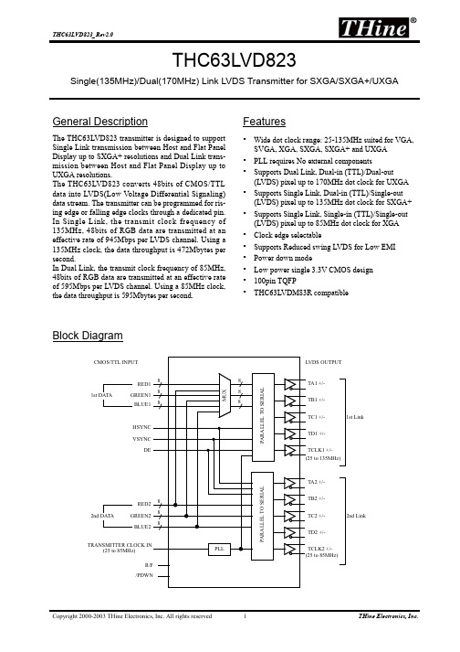
THC63LVD823Single(135MHz)/Dual(170MHz) Link LVDS Transmitter for SXGA/SXGA+/UXGAGeneral DescriptionThe THC63LVD823 transmitter is designed to support Single Link transmission between Host and Flat Panel Display up to SXGA+ resolutions and Dual Link trans-mission between Host and Flat Panel Display up to UXGA resolutions.The THC63LVD823 converts 48bits of CMOS/TTL data into LVDS(Low Voltage Differential Signaling)data stream. The transmitter can be programmed for ris-ing edge or falling edge clocks through a dedicated pin.In Single Link, the transmit clock frequency of 135MHz, 48bits of RGB data are transmitted at an effective rate of 945Mbps per LVDS channel. Using a 135MHz clock, the data throughput is 472Mbytes per second.In Dual Link, the transmit clock frequency of 85MHz,48bits of RGB data are transmitted at an effective rate of 595Mbps per LVDS channel. Using a 85MHz clock,the data throughput is 595Mbytes per second.Features•Wide dot clock range: 25-135MHz suited for VGA,SVGA, XGA, SXGA, SXGA+ and UXGA•PLL requires No external components•Supports Dual Link, Dual-in (TTL)/Dual-out(LVDS) pixel up to 170MHz dot clock for UXGA•Supports Single Link, Dual-in (TTL)/Single-out (LVDS) pixel up to 135MHz dot clock for SXGA+•Supports Single Link, Single-in (TTL)/Single-out (LVDS) pixel up to 85MHz dot clock for XGA •Clock edge selectable•Supports Reduced swing LVDS for Low EMI •Power down mode•Low power single 3.3V CMOS design •100pin TQFP•THC63LVDM83R compatibleBlock DiagramP A R A L L E L T O S E R I A LPLLTA1 +/-TB1 +/-TC1 +/-TD1 +/-TCLK1 +/-R/F /PDWN(25 to 135MHz)1st Link8RED1GREEN1BLUE1HSYNC VSYNCDERED2GREEN2BLUE2TRANSMITTER CLOCK IN(25 to 85MHz)1st DATA2nd DATACMOS/TTL INPUTP A R A L L E L T O S E R I A LTA2 +/-TB2 +/-TC2 +/-TD2 +/-TCLK2 +/-M U X88888888(25 to 85MHz)2nd LinkLVDS OUTPUTPin OutB15 B16 B17 R20 R21 R22 R23 R24 R25 R26 R27 VCC GND G20 G21 G22 G23 G24 G25 G26 G27 B20 B21 B22 B23767778798081828384858687888990919293949596979899100LVDS GNDTA1-TA1+TB1-TB1+LVDS VCCTC1-TC1+TCLK1-TCLK1+TD1-TD1+LVDS GNDTA2-TA2+TB2-TB2+LVDS VCCTC2-TC2+TCLK2-TCLK2+TD2-TD2+LVDS GND50494847464544434241403938373635343332313029282726 B24B25VCCGNDB26B27HSYNCVSYNCDECLKINR/FRSTEST1TEST2MODE1MODEOE6/8/PDWNTEST3TEST4TEST5PLLGNDPLLVCCPLLGND 123456789111121314151617181922122232425 B14B13B12GNDVCCB11B1G17G16G15G14G13G12G11G1R17R16R15R14GNDVCCR13R12R11R10 757473727176968676665646362616595857565554535251Pin DescriptionPin Name Pin #Type DescriptionTA1+, TA1-48, 49LVDS OUT The 1st Link. The 1st pixel output data when Dual Link.TB1+, TB1-46, 47LVDS OUT TC1+, TC1-43, 44LVDS OUT TD1+, TD1-39, 40LVDS OUT TCLK1+, TCLK1-41, 42LVDS OUT LVDS Clock Out for 1st Link.TA2+, TA2-36, 37LVDS OUT The 2nd Link. These pins are disabled when Single Link.TB2+, TB2-34, 35LVDS OUT TC2+, TC2-31, 32LVDS OUT TD2+, TD2-27, 28LVDS OUT TCLK2+, TCLK2-29, 30LVDS OUTLVDS Clock Out for 2nd Link.R17 ~ R1060, 59, 58, 57, 54, 53, 52, 51IN The 1st Pixel Data Inputs.G17 ~ G1068, 67, 66, 65, 64, 63, 62, 61IN B17 ~ B1078, 77, 76, 75, 74, 73, 70, 69IN R27 ~ R2086, 85, 84, 83, 82, 81, 80, 79IN The 2nd Pixel Data Inputs.G27 ~ G2096, 95, 94, 93, 92, 91, 90, 89IN B27 ~ B206, 5, 2, 1, 100, 99, 98, 97IN DE 9IN Data Enable Input.VSYNC 8IN Vsync Input.HSYNC 7IN Hsync Input.CLKIN 10IN Clock Input.TEST1, TEST513, 22OUT Test Pins.TEST3, TEST420, 21IN Test Pins, must be L for normal operation.TEST214IN Test Pins, must be H for normal operation./PDWN 19IN H: Normal operation,L: Power down (all outputs are Hi-Z)6/818IN 6bit/8bit color select.H: 6bit (TDx+/- are GND), L: 8bit.OE17INOutput enable.H: Output enable, L: Output disable (all outputs are Hi-Z)MODE1, MODE015, 16INRS 12INLVDS swing range select.H: Normal range, L: Reduced range.Pixel Data Mode.MODE1MODE0ModeL L Dual Link (Dual-in/Dual-out)L H Single Link (Dual-in/Single-out)HHSingle Link (Single-in/Single-out)Absolute Maximum Ratings 1Electrical Characteristics CMOS/TTL DC SpecificationsV CC = 3.0V ~ 3.6V , Ta = -10 ~ +70R/F 11IN Input Clock Triggering Edge Select.H: Rising edge, L: Falling edgeVCC 3, 55, 71, 87Power Power Supply Pins for TTL inputs, output and digital circuitry.GND 4, 56, 72, 88Ground Ground Pins for TTL inputs, outputs and digital circuitry.LVDS VCC 33, 45Power Power Supply Pins for LVDS Outputs.LVDS GND 26, 38, 50Ground Ground Pins for LVDS Outputs.PLL VCC 24Power Power Supply for PLL circuitry.PLL GND23, 25GroundGround Pin for PLL circuitry.Supply Voltage (V CC )-0.3V ~ +4.0V CMOS/TTL Input V oltage -0.3V ~ (V CC + 0.3V)CMOS/TTL Output Voltage -0.3V ~ (V CC + 0.3V)LVDS Driver Output Voltage -0.3V ~ (V CC + 0.3V)Output Current -30mA ~ 30mA Junction Temperature +125Storage Temperature Range -55 ~ +125Lead Temperature (Soldering, 4sec)+260Maximum Power Dissipation @+25 1.0W1.“Absolute Maximum Ratings” are those valued beyond which the safety of the device can not be guaranteed. They are not meant to imply that the device should be operated at these limits. The tables of “Electrical Characteristics” specify conditions for device operation.Symbol ParameterConditions Min.Typ.Max.Units V IH High Level Input Voltage 2.0V CC V V IL Low Level Input V oltage GND0.8V I INCInput CurrentµAPin Name Pin #Type Description°C°C °C °C °C°C °C0V V IN V CC≤≤10±LVDS Transmitter DC SpecificationsV CC = 3.0V ~ 3.6V , Ta = -10 ~ +70Supply CurrentV CC = 3.0V ~ 3.6V , Ta = -10 ~ +70(*) VESA is a trademark of the Video Electronics Standards Association.SymbolParameterConditionsMin.Typ.Max.Units VOD Differential Output Voltage RL=100ΩNormal swing 250350450mV Reduced swing100200300mV ∆VOD Change in VOD between complementary output states RL=100Ω35mV VOC Common Mode Voltage 1.1251.251.375V ∆VOC Change in VOC between complementary output states 35mV I OS Output Short Circuit Current VOUT=0V , RL=100Ω-24mA I OZOutput TRI-State current/PDWN=0V , VOUT=0V to VCCµASymbolParameterCondition(*)Typ.Max.UnitsI TCCGTransmitter SupplyCurrent(256 Gray Scale Pattern)VESA SXGA ( 60Hz )CLKIN=54MHzMODE<1:0>=LH RL=100Ω,CL=5pF VCC=3.3V 5058mAVESA UXGA ( 60Hz )CLKIN=81MHz MODE<1:0>=LL RL=100Ω,CL=5pF VCC=3.3V 7889mAI TCCWTransmitter SupplyCurrent(Double Checker Pattern)VESA SXGA ( 60Hz )CLKIN=54MHz MODE<1:0>=LH RL=100Ω,CL=5pF VCC=3.3V 5361mAVESA UXGA ( 60Hz )CLKIN=81MHzMODE<1:0>=LL RL=100Ω,CL=5pF VCC=3.38699mAI TCCSTransmitter Power Down Supply Current/PDWN = L 10µA°C °C°C °C10±256 Gray Scale PatternCLKINRx0/Gx0/Bx0Rx1/Gx1/Bx1Rx2/Gx2/Bx2Rx3/Gx3/Bx3Rx4/Gx4/Bx4Rx5/Gx5/Bx5Rx6/Gx6/Bx6Rx7/Gx7/Bx7x=1,2DEDouble Checker Pattern CLKINR1n/G1n/B1nR2n/G2n/B2nn=0~7DESwitching CharacteristicsV CC = 3.0V ~ 3.6V, Ta = -10 ~ +70 Symbol Parameter Min.Typ.Max.Units t TCIT CLK IN Transition time 5.0ns t TCIP CLK IN Period11.7640.0ns t TCH CLK IN High Time0.35t TCIP0.5t TCIP0.65t TCIP ns t TCL CLK IN Low Time0.35t TCIP0.5t TCIP0.65t TCIP ns t TS TTL Data Setup to CLK IN 2.5ns t TH TTL Data Hold from CKL IN0.0nst TCOP CLK OUT PeriodDual Link11.7640.0ns Single Link7.420.0nst LVT LVDS Transition Time0.5ns t TOP1Output Data Position0 (t TCOP = 7.4ns)-0.150.0+0.15nst TOP0Output Data Position1 (t TCOP = 7.4ns)ns t TOP6Output Data Position2 (t TCOP = 7.4ns)ns t TOP5Output Data Position3 (t TCOP = 7.4ns)ns t TOP4Output Data Position4 (t TCOP = 7.4ns)ns t TOP3Output Data Position5 (t TCOP = 7.4ns)ns t TOP2Output Data Position6 (t TCOP = 7.4ns)nst TPLL Phase Lock Loop Set10.0ms t OE OE High to Data Valid50nst CK12Skew Time between TCLK1+ and TCLK2+0.5ns°C°Ct TCOP7--------------0.15–t TCOP7--------------t TCOP7--------------0.15+2t TCOP7--------------0.15–2t TCOP7--------------2t TCOP7--------------0.15+3t TCOP7--------------0.15–3t TCOP7--------------3t TCOP7--------------0.15+4t TCOP7--------------0.15–4t TCOP7--------------4t TCOP7--------------0.15+5t TCOP7--------------0.15–5t TCOP7--------------5t TCOP7--------------0.15+6t TCOP7--------------0.15–6t TCOP7--------------6t TCOP7--------------0.15+AC Timing Diagrams TTL Input5pF20%80%20%80%t LVT t LVTCLK INLVDS Output90%10%90%10%t TCIT t TCITV diff100ΩV diff=(TA+)-(TA-) TA+TA-LVDS Output LoadAC Timing Diagrams TTL InputsR/F = LR/F = HCLK INRxn GxnBxnn = 0~7Phase Lock Loop Set TimeVCC3.0V2.0Vt TPLLCLKIN/PDWNTCLKx+/-V diff =0VHsync Vsync DEPower Up Sequence3.0VPDVCCGNDVCCGNDVCC PVCC LVCCGNDPD pin must be High after VCC voltage is 3.0V .1)Sequence1VCC/2PDVCCGNDt PDVCC/2VCCGNDVCC PVCC LVCCt PW1) t PW < 10msec 2) t PD > t PW2)Sequence2Power Up Sequence must be Sequence1 or Sequence2.V diff = 0V Tyx+/-AC Timing Diagrams LVDS OutputsTyx6Tyx5Tyx4Tyx3Tyx2Tyx1Tyx0Tyx6Tyx5Tyx4Tyx3Tyx2Tyx1V diff = 0Vt TOP2t TOP3t TOP4t TOP5t TOP6t TOP0t TOP1t TCOPTCLKx+x = 1,2y = A,B,C,DV diff = 0Vt CK12TCLK1+V diff = 0VTCLK2+Note:V diff = (Tyx+) - (Tyx-) , (TCLKx+) - (TCLKx-)Pixel Map Table for Single/Dual LinkTFT Panel DataLSB 24Bit18Bit823 TTL Input Pin 1st Pixel DataR10-MSB R11R12R13R14R15R16R17-R10R11R12R13R14R15LSBMSB G11G12G13G14G15G16G17-G10G11G12G13G14G15 G10-LSBMSB B11B12B13B14B15B16B17-B10B11B12B13B14B15B10-R10R11R12R13R14R15R16R17G11G12G13G14G15G16G17G10B11B12B13B14B15B16B17B10TFT Panel DataLSB24Bit18Bit823 TTL Input Pin2nd Pixel DataR20-MSBR21R22R23R24R25R26R27-R20R21R22R23R24R25LSBMSBG21G22G23G24G25G26G27-G20G21G22G23G24G25G20-LSBMSBB21B22B23B24B25B26B27-B20B21B22B23B24B25B20-R20R21R22R23R24R25R26R27G21G22G23G24G25G26G27G20B21B22B23B24B25B26B27B20TTL Data Inputs Timing Diagrams in Dual Link TA1+/-R16’R15’R14’R13’R12’G12R17R16R15R14R13R12G12’’TB1+/-G17’G16’G15’G14’G13’B13B12G17G16G15G14G13B13’’TC1+/-HSYNC’B17’B16’B15’B14’DEVSYNC HSYNCB17B16B15B14DE’’TD1+/-B10’G11’G10’R11’R10’L B11B10G11G10R11R10L’’TA2+/-R26’R25’R24’R23’R22’G22R27R26R25R24R23R22G22’’TB2+/-G27’G26’G25’G24’G23’B23B22G27G26G25G24G23B23’’TC2+/-B27’B26’B25’B24’B27B26B25B24TD2+/-B20’G21’G20’R21’R20’L B21B20G21G20R21R20L’’TCLK1+TCLK2+(Dual-in / Dual-out Mode)Previous Cycle Current CycleHSYNC’DEVSYNC HSYNCDE’’TTL Data Inputs Timing Diagrams in Single Link(Dual-in / Single-out Mode)Previous Cycle Current Cycle(2nd Pixel Data)(1st Pixel Data)TCLK1+TA1+/-R26’R25’R24’R23’R22’G12R17R16R15R14R13R12G22’’TB1+/-G27’G26’G25’G24’G23’B13B12G17G16G15G14G13B23’’TC1+/-HSYNC’B27’B26’B25’B24’DE VSYNC HSYNC B17B16B15B14DE’’TD1+/-B20’G21’G20’R21’R20’L B11B10G11G10R11R10L’’Package1.2M A XUNIT:mm1.00T Y PNotes to Users:1.The contents of this data sheet are subject to change without prior notice.2.Circuit diagrams shown in this data sheet are examples of application. Therefore, please pay sufficient attentionwhen designing circuits. Even if there are incorrect descriptions, we are not responsible for any problem due to them. Please note that incorrect descriptions sometimes cannot be corrected immediately if found.3.Our copyright and know-how are included in this data sheet. Duplication of the data sheet and disclosure to otherpersons are strictly prohibited without our permission.4.We are not responsible for any problems of industrial proprietorship occurring during THC63LVD823 use, exceptfor those directly related to THC63LVD823’s structure, manufacture or functions. THC63LVD823 is designed on the premise that it should be used for ordinary electronic devices. Therefore, it shall not be used for applications that require extremely high-reliability (space equipment, nuclear control equipment, medical equipment that affects peo-ple’s lives, etc.). In addition, when using THC63LVD823 for traffic signals, safety devices and control/safety units in transportation equipment, etc., appropriate measures should be taken.5.We are making the utmost effort to improve the quality and reliability of our products. However, there is a veryslight possibility of failure in semiconductor devices. To avoid damage to social or official organizations, much care should be taken to provide sufficient redundancy and fail-safe design.6.No radiation-hardened design is incorporated in THC63LVD823.7.Judgment on whether THC63LVD823 comes under strategic products prescribed by the Foreign Exchange and For-eign Trade Control Law is the user’s responsibility.8.This technical document was provisionally created during development of THC63LVD823, so there is a possibilityof differences between it and the product’s final specifications. When designing circuits using THC63LVD823, be sure to refer to the final technical documents.THine Electronics, Inc.Wakamatsu Bldg, 6F3-3-6, Nihombashi-Honcho,Chuo-ku, Tokyo, 103-0023 JapanTel: 81-3-3270-0666Fax: 81-3-3270-0688。
ADL5513资料

元器件交易网
ADL5513
TABLE OF CONTENTS
Features .............................................................................................. 1 Applications....................................................................................... 1 Functional Block Diagram .............................................................. 1 General Description ......................................................................... 1 Revision History ............................................................................... 2 Specifications..................................................................................... 3 Absolute Maximum Ratings............................................................ 6
Rev. PrA | Page 2 of 12
元器件交易网
Preliminary Technical Data
NACEW3R3M6.35x5.5TR13F中文资料

Surface Mount Aluminum Electrolytic Capacitors
FEATURES • CYLINDRICAL V-CHIP CONSTRUCTION • WIDE TEMPERATURE -55 ~ +105OC • ANTI-SOLVENT (2 MINUTES) • DESIGNED FOR REFLOW ttSOLDERING CHARACTERISTICS
25 32 0.14 0.16 25 2 4
35 44 0.12 0.14 35 2 3
50 63 0.10 0.12 50 2 3
63 79 0.12 0.12 63 2 3
100 125 0.10 0.10 100 2 -
Within ± 25% of initial measured value Less than 200% of specified max. value Less than specified max. value
PRECAUTIONS
RIPPLE CURRENT FREQUENCY CORRECTION FACTOR
Frequency (Hz) Correction Factor f < 100 0.8 100 > f < 1K 1K > f < 10K f > 100K 1.0 1.3 1.5
10
NIC COMPONENTS
Surface Mount Aluminum Electrolytic Capacitors
STANDARD PRODUCT AND CASE SIZE TABLE DφxL (mm)
Cap. (µF) 0.1 0.22 0.33 0.47 1.0 2.2 3.3 4.7 10 22 33 47 100 150 220 330 470 Code R10 R22 R33 R47 1R0 2R2 3R3 4R7 100 220 330 470 101 151 221 331 471 6.3 4x5.5* 5x5.5* 5x5.5* 6.3x5.5* 6.3x5.5* 6.3x6.3* 6.3x8* 8x10.5 10 5x5.5* 5x5.5* 6.3x5.5* 6.3x6.3* 6.3x8* 8x10.5* Working Voltage (Vdc) 16 25 35 4x5.5* 4x5.5* 4x5.5* 5x5.5* 5x5.5* 5x5.5* 6.3x5.5* 6.3x5.5* 6.3x5.5* 6.3x5.5* 6.3x6.3* 6.3x5.5* 6.3x6.3* 6.3x6.3* 6.3x5.5* 6.3x8* 6.3x8 8x10.5* 6.3x8* 8x10.5* 10x8* 8x10.5* 6.3x8* 8x10.5 10x8* 8x10.5* 8x10.5* 10x10.5 10x8 50 63 4x5.5* 4x5.5* 4x5.5* 4x5.5* 4x5.5* 4x5.5* 4x5.5* 4x5.5* 4x5.5* 4x5.5* 4x5.5* 4x5.5* 4x5.5* 5x5.5* 5x5.5* 5x5.5* 6.3x5.5* 6.3x5.5* 6.3x6.3* 6.3x8* 6.3x8* 8x10.5* 6.3x8* 8x10.5* 8x10.5* 10x10.5* 10x10.5 16x17 12.5x14 16x17 100 4x6.3* 6.3x6.3* 6.3x6.3* 6.3x6.3* 6.3x8* 8x10.5* 10x10.5* 12.5x14 16x17 -
NACE1500M25V4X5.5TR13F中文资料

1®NIC COMPONENTS CORP. ww www www www Surface Mount Aluminum Electrolytic CapacitorsNACE SeriesFEATURES•CYLINDRICAL V-CHIP CONSTRUCTION• LOW COST, GENERAL PURPOSE, 2000 HOURS AT 85O C •NEW EXP ANDED CV RANGE (up to 6800µF)•ANTI-SOLVENT (2 MINUTES)•DESIGNED FOR AUTOMATIC MOUNTING AND REFLOW SOLDERINGCHARACTERISTICS*See standard products and case size table for items available in 10% toleranceRated Voltage Range 4.0 ~ 100Vdc Rate Capacitance Range 0.1 ~ 6,800µFOerating Temp. Range -40°C ~ +85°CCapacitance Tolerance ±20% (M), ±10%Max. Leakage Current After 2 Minutes @ 20°C0.01CV or 3µA whichever is greaterTan δ @120Hz/20°C W.V . (Vdc) 4.0 6.31016253550631003mm Dia.0.400.350.240.190.160.140.14--4 ~ 6.3mm Dia.0.350.260.200.160.140.120.100.100.108x6.5mm Dia.-0.250.260.200.160.140.12-0.108mm Dia. ~ upC<1000µF 0.400.300.240.200.160.140.120.120.10C<1500µF -0.310.250.21-0.15---C<2200µF -0.320.32-0.18----C<3300µF -0.34-0.24-----C<4700µF --0.36------C<6800µF -0.40-------Low Temperature StabilityImpedance Ratio @ 120HzW.V . (Vdc) 4.0 6.3101625355063100Z-25°C/Z+20°C 733222222Z-40°C/Z+20°C 1586443333Load Life Test85°C 2,000 HoursCapacitance Change Within ± 25% of initial measured valueTan δLess than 200% of specifi ed max. valueLeakage Current Less than specifi ed max. value NACE 101 M 16V 6.3x5.5 TR 13 FRoHS Compliant97% Sn (min.), 3% Bi (max.) 330mm (13”) Reel Tape & Reel Size in mm Working VoltageTolerance Code M=20%, K=10% Capacitance Code in µF , fi rst 2 digits are signifi cant Third digit is no. of zeros, “R” indicates decimal for values under 10µF SeriesPART NUMBER SYSTEMRoHSCompliantincludes all homogeneous materials *See Part Number System for Details PRECAUTIONSPlease review the notes on correct use, safety and precautions found on pages T10 & T11of NIC’s Electrolytic Capacitor catalog . Also found at /precautionsIf in doubt or uncertainty, please review your specifi c application - process details withNIC’s technical support personnel: tpmg@2MAXIMUM RIPPLE CURRENT O MAXIMUM ESRO Surface Mount Aluminum Electrolytic CapacitorsNACE SeriesSTANDARD PRODUCT AND CASE SIZE TABLE DφxL (mm)*Items available in optional 10% toleranceSurface Mount Aluminum Electrolytic Capacitors NACE Series+ -3。
- 1、下载文档前请自行甄别文档内容的完整性,平台不提供额外的编辑、内容补充、找答案等附加服务。
- 2、"仅部分预览"的文档,不可在线预览部分如存在完整性等问题,可反馈申请退款(可完整预览的文档不适用该条件!)。
- 3、如文档侵犯您的权益,请联系客服反馈,我们会尽快为您处理(人工客服工作时间:9:00-18:30)。
TLRD135
Unit in mm
Electro-Optical Characteristics (T Forward Voltage Reverse Current TLRD135 Luminous Intensity TLRD135(NP) Peak Emission Wavelength Spectral Line Half Width Symbol VF IR IV (NOTE) λp ∆λ Test Condition IF = 20 mA VR = 4 V IF = 20 mA (NP) IF = 20 mA IF = 20 mA Min. – – 85 100 – – Typ. 1.8 – – – 660 25 Max. 2.2 50 – mcd 360 – – nm nm Unit V µA
2/2
TOSHIBA CORPORATION
The information contained here is subject to change without notice. The information contained herein is presented only as guide for the applications of our products. No responsibility is assumed by TOSHIBA for any infringements of patents or other rights of the third parties which may result from its use. No license is granted by implication or otherwise under any patent or patent rights of TOSHIBA or others. These TOSHIBA products are intended for usage in general electronic equipments (office equipment, communication equipment, measuring equipment, domestic electrification, etc.) Please make sure that you consult with us before you use these TOSHIBA products in equipments which require high quality and/or reliability, and in equipments which could have major impact to the welfare of human life (atomic energy control, spaceship, traffic signal, combustion control, all types of safety devices, etc.). TOSHIBA cannot accept liability to any damage which may occur in case these TOSHIBA products were used in the mentioned equipments without prior consultation with TOSHIBA.
TOSHIBA CORPORATION
1/2
元器件交易网
TLRD135
Precaution Please be careful of the following: 1. Soldering temperature: 260°C MAX. Soldering time: 3 sec MAX. (Soldering portion of lead: up to 2mm from the body of the device). 2. If the lead is formed, the lead should be formed up to 5mm from the body of the device without forming stress. Soldering shall be performed after lead forming.
(NOTE) Rank selection carried out under next range respectively, although it needs ±15% additional for guaranteed limits. N:100-200mcd, P:180-360mcd, Q:320-640mcd.
元器件交易网
TOSHIBA
LED Lamp GaAlAs Red Light Emission
Panel Circuit Indicator 5 mm Diameter (T1-3/4) • GaAlAs Red LED • All Plastic Mold Type • Colorless Clear Lens - Wide Radiation Pattern • Low Drive Current, High Intensity Red Light Emission - Recommended Forward Current: IF = 15 ~ 20 mA (DC) • All Plastic Molded Lens - Provides an Excellent ON-OFF Contrast Ratio • Fast Response Time - Capable of Pulse Operation • Straight Lead (no stand-off) • Applications: - Indoor Indicator Maximum Ratings (Ta = 25°C)
Characteristic Forward Current (DC) Reverse Voltage Power Dissipation Operating Temperature Range Storage Temperature Range Symbol IF VR PD Topr Tstg Rating 50 4 125 −30 ~ 85 −40 ~ 100 Unit mA V mW °C °C