4A003
万能遥控器代码一览表
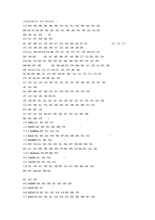
海尔 103.112 .118 .119. 150.151.152 .153 .154 .155 .156. 182. 183. 184. 193.
194.213 .228
海信000.006.007. 008.010.014 .015. 025. 045.046.103. 105.
华发HUAFA 007.016.025
华强HUAQIANG 033.053.056.079..
杂牌机036.044.114…
ZAPAIJI
飞跃011.016.023.024.025.040.043…
FEIYUE-
飞浪016.025
FEILANG
南宝016.025.033.053.056.009.057.058.059<).
创维011. 025.033.045.046.060 .070.017.072. 073. 074. 079. 083.010 .107.
108.109162163.164 .165 .166 .167. 168. 169. 177. 224.225. 235.246
熊猫001. 011.016. 021. 022.023.024 .025. 026.028.033 .040 .043. 053.
011.025.016
松柏
SONGBA
016.025
三元
SANYUAN
003.011.016.018.023.024.025.040.043
三键
SANJIAN
033.053.056.079
泰山
TAISHAN
011.016.025.042.038.031.030.029.028.027
ADP3654 高速双路 4A MOSFET 驱动器 数据手册 Rev. A说明书

High Speed, Dual, 4 A MOSFET DriverData SheetADP3654Rev. A Document Feedback Information furnished by Analog Devices is believed to be accurate and reliable. However , no responsibility is assumed by Analog Devices for its use, nor for any infringements of patents or other rights of third parties that may result from its use. Specifications subject to change without notice. No license is granted by implication or otherwise under any patent or patent rights of Analog Devices. T rademarks and registered trademarks are the property of their respective owners.One Technology Way, P.O. Box 9106, N orwood, MA 02062-9106, U.S.A. Tel: 781.329.4700 ©2010–2015 Analog Devices, Inc. All rights reserved. Technical Support FEATURESIndustry-standard-compatible pinout High current drive capabilityPrecise UVLO comparator with hysteresis 3.3 V-compatible inputs10 ns typical rise time and fall time at 2.2 nF load Matched propagation delays between channels Fast propagation delay 4.5 V to 18 V supply voltage Parallelable dual outputsRated from −40°C to +125°C junction temperatureThermally enhanced packages, 8-lead SOIC_N_EP and 8-lead MINI_SO_EPAPPLICATIONSAC-to-dc switch mode power supplies DC-to-dc power supplies Synchronous rectification Motor drivesGENERAL DESCRIPTIONThe ADP3654 high current and dual high speed driver is capable of driving two independent N-channel power MOSFETs. The driver uses the industry-standard footprint but adds high speed switching performance.The wide input voltage range allows the driver to be compatible with both analog and digital PWM controllers.Digital power controllers are powered from a low voltagesupply, and the driver is powered from a higher voltage supply. The ADP3654 driver adds UVLO and hysteresis functions, allowing safe startup and shutdown of the higher voltage supply when used with low voltage digital controllers.The driver is available in thermally enhanced SOIC_N_EP and MINI_SO_EP packaging to maximize high frequency and current switching in a small printed circuit board (PCB) area.FUNCTIONAL BLOCK DIAGRAMOUTAVDDOUTBNCINA PGND INBNC09054-001Figure 1.ADP3654* Product Page Quick Links Last Content Update: 08/30/2016Comparable PartsView a parametric search of comparable partsDocumentationData Sheet•ADP3654: High Speed, Dual, 4 A MOSFET DriverDesign Resources•ADP3654 Material Declaration•PCN-PDN Information•Quality And Reliability•Symbols and FootprintsDiscussionsView all ADP3654 EngineerZone DiscussionsSample and BuyVisit the product page to see pricing optionsTechnical SupportSubmit a technical question or find your regional support number* This page was dynamically generated by Analog Devices, Inc. and inserted into this data sheet. Note: Dynamic changes to the content on this page does not constitute a change to the revision number of the product data sheet. This content may be frequently modified.ADP3654Data SheetRev. A | Page 2 of 13TABLE OF CONTENTSFeatures .............................................................................................. 1 Applications ....................................................................................... 1 General Description ......................................................................... 1 Functional Block Diagram .............................................................. 1 Revision History ............................................................................... 2 Specifications ..................................................................................... 3 Timing Diagrams .......................................................................... 3 Absolute Maximum Ratings ............................................................ 4 ESD Caution .................................................................................. 4 Pin Configuration and Function Descriptions ............................. 5 Typical Performance Characteristics ............................................. 6 Test Circuit .........................................................................................8 Theory of Operation .........................................................................9 Input Drive Requirements (INA and INB) ................................9 Low-Side Drivers (OUTA, OUTB) .............................................9 Supply Capacitor Selection ..........................................................9 PCB Layout Considerations .........................................................9 Parallel Operation ...................................................................... 10 Thermal Considerations ............................................................ 10 Outline Dimensions ....................................................................... 12 Ordering Guide .. (13)REVISION HISTORY8/15—Rev. 0 to Rev. AChanges to Figure 5 .......................................................................... 6 Updated Outline Dimensions ....................................................... 12 Changes to Ordering Guide . (13)8/10—Revision 0: Initial VersionData SheetADP3654Rev. A | Page 3 of 13SPECIFICATIONSV DD = 12 V , T J = −40°C to +125°C, unless otherwise noted.1 Table 1.Parameter Symbol Test Conditions/Comments Min Typ Max Unit SUPPLYSupply Voltage Range V DD4.5 18V Supply Current I DD No switching 1.2 3 mA UVLOTurn-On Threshold Voltage V UVLO_ON V DD rising, T J = 25°C, see Figure 3 3.8 4.2 4.5 V Turn-Off Threshold Voltage V UVLO_OFF V DD falling, T J = 25°C, see Figure 3 3.5 3.9 4.3 V Hysteresis0.3 V DIGITAL INPUTS (INA, INB)Input Voltage High V IH See Figure 2 2.0 V Input Voltage Low V IL See Figure 2 0.8 V Input CurrentI IN 0 V < V IN < V DD −20 +20 µA Internal Pull-Up/Pull-Down Current 6 µA OUTPUTS (OUTA, OUTB)Output Resistance, Unbiased VDD = PGND 80 kΩ Peak Source Current See Figure 14 4 A Peak Sink Current See Figure 14 −4 A SWITCHING TIMEOUTA and OUTB Rise Time t RISE C LOAD = 2.2 nF, see Figure 2 10 25 ns OUTA and OUTB Fall Timet FALL C LOAD = 2.2 nF, see Figure 2 10 25 ns OUTA and OUTB Rising Propagation Delay t D1 C LOAD = 2.2 nF, see Figure 2 14 30 ns OUTA and OUTB Falling Propagation Delay t D2 C LOAD = 2.2 nF, see Figure 2 22 35 ns Delay Matching Between Channels2 ns1All limits at temperature extremes guaranteed via correlation using standard statistical quality control (SQC) methods.TIMING DIAGRAMS09054-002Figure 2. Output Timing Diagram09054-003Figure 3. UVLO FunctionADP3654Data SheetRev. A | Page 4 of 13ABSOLUTE MAXIMUM RATINGSTable 2.Parameter RatingVDD−0.3 V to +20 V OUTA, OUTBDC−0.3 V to V DD + 0.3 V <200 ns −2 V to V DD + 0.3 V INA, INB −0.3 V to V DD + 0.3 V ESDHuman Body Model (HBM)3.5 kV Field Induced Charged Device Model (FICDM)SOIC_N_EP 1.5 kV MINI_SO_EP1.0 kV θJA , JEDEC 4-Layer BoardSOIC_N_EP 1 59°C/W MINI_SO_EP 143°C/WJunction Temperature Range −40°C to +150°C Storage Temperature Range −65°C to +150°C Lead TemperatureSoldering (10 sec) 300°C Vapor Phase (60 sec) 215°C Infrared (15 sec)260°C1θJA is measured per JEDEC standards, JESD51-2, JESD51-5, and JESD51-7, as appropriate with the exposed pad soldered to the PCB.Stresses at or above those listed under Absolute Maximum Ratings may cause permanent damage to the product. This is a stress rating only; functional operation of the product at these or any other conditions above those indicated in the operational section of this specification is not implied. Operation beyond the maximum operating conditions for extended periods may affect product reliability.ESD CAUTIONData SheetADP3654Rev. A | Page 5 of 13PIN CONFIGURATION AND FUNCTION DESCRIPTIONSNC 1INA 2PGND 3INB 4NC8OUTA7VDD6OUTB 5ADP3654TOP VIEW(Not to Scale)NOTES1. NC = NO CONNECT.2.THE EXPOSED PAD OF THE PACKAGE IS NOT DIRECTLY CONNECTED TO ANY PIN OF THE PACKAGE, BUT IT ISELECTRICALLY AND THERMALLY CONNECTED TO THE DIE SUBSTRATE, WHICH IS THE GROUND OF THE DEVICE. IT IS RECOMMENDED TO HAVE THE EXPOSED PAD AND THE PGND PIN CONNECTED ON THE PCB.09054-004Figure 4. Pin ConfigurationTable 3. Pin Function DescriptionsPin No. Mnemonic Description 1 NC No Connect.2 INA Input Pin for Channel A Gate Driver.3 PGND Ground. This pin should be closely connected to the source of the power MOSFET.4 INB Input Pin for Channel B Gate Driver.5 OUTB Output Pin for Channel B Gate Driver.6 VDD Power Supply Voltage. Bypass this pin to PGND with a ~1 µF to 5 µF ceramic capacitor.7 OUTA Output Pin for Channel A Gate Driver.8 NC No Connect.9EPADExposed Pad. The exposed pad of the package is not directly connected to any pin of the package, but it is electrically and thermally connected to the die substrate, which is the ground of the device. It is recommended to have the exposed pad and the PGND pin connected on the PCB.ADP3654Data SheetRev. A | Page 6 of 13TYPICAL PERFORMANCE CHARACTERISTICSV DD = 12 V , T J = 25°C, unless otherwise noted.3456789–50–30–101030507090110130TEMPERATURE (°C)U V L O (V )09054-005Figure 5. UVLO vs. Temperature02468101214–50–30–101030507090110130TEMPERATURE (°C)t FALL t RISET I M E (n s )09054-006Figure 6. Rise and Fall Times vs. Temperature102030405060–50–30–101030507090110130TEMPERATURE (°C)T I M E (n s )09054-007Figure 7. Propagation Delay vs. Temperature 051015202505101520V DD (V)T I M E (n s )t FALLt RISE09054-008Figure 8. Rise and Fall Times vs. V DD01020304050607005101520t D2t D1V DD (V)T I M E (n s )09054-009Figure 9. Propagation Delay vs. V DD09054-010Figure 10. Typical Rise Propagation DelayData SheetADP3654Rev. A | Page 7 of 1309054-011Figure 11. Typical Fall Propagation Delay 09054-012Figure 12. Typical Rise Time09054-013Figure 13. Typical Fall TimeADP3654Data SheetRev. A | Page 8 of 13TEST CIRCUITLOAD09054-014Figure 14. Test CircuitData SheetADP3654Rev. A | Page 9 of 13THEORY OF OPERATIONThe ADP3654 dual driver is optimized for driving twoindependent enhancement N-channel MOSFETs or insulated gate bipolar transistors (IGBTs) in high switching frequency applications.These applications require high speed, fast rise and fall times, as well as short propagation delays. The capacitive nature of the aforementioned gated devices requires high peak current capability as well.09054-015Figure 15. Typical Application CircuitINPUT DRIVE REQUIREMENTS (INA AND INB)The ADP3654 is designed to meet the requirements of modern digital power controllers; the signals are compatible with 3.3 V logic levels. At the same time, the input structure allows for input voltages as high as V DD .An internal pull-down resistor is present at the input, which guarantees that the power device is off in the event that the input is left floating.LOW-SIDE DRIVERS (OUTA, OUTB)The ADP3654 dual drivers are designed to drive ground referenced N-channel MOSFETs. The bias is internally connected to the V DD supply and PGND.When ADP3654 is disabled, both low-side gates are held low. Internal impedance is present between the OUTA pin and GND and between the OUTB pin and GND; this feature ensures that the power MOSFET is normally off when bias voltage is not present.When interfacing ADP3654 to external MOSFETs, the designer should consider ways to make a robust design that minimizes stresses on both the driver and the MOSFETs. These stresses include exceeding the short time duration voltage ratings on the OUTA and OUTB pins, as well as the external MOSFET. Power MOSFETs are usually selected to have a low on resistance to minimize conduction losses, which usually implies a large input gate capacitance and gate charge.SUPPLY CAPACITOR SELECTIONFor the supply input (V DD ) of the ADP3654, a local bypass capacitor is recommended to reduce the noise and to supply some of the peak currents that are drawn.An improper decoupling can dramatically increase the rise times because excessive resonance on the OUTA and OUTB pins can, in some extreme cases, damage the device, due to inductive overvoltage on the VDD, OUTA, or OUTB pin. The minimum capacitance required is determined by the size of the gate capacitances being driven, but as a general rule, a 4.7 µF, low ESR capacitor should be used. Multilayer ceramic chip (MLCC) capacitors provide the best combination of low ESR and small size. Use a smaller ceramic capacitor (100 nF) with a better high frequency characteristic in parallel to the main capacitor to further reduce noise.Keep the ceramic capacitor as close as possible to the ADP3654 device and minimize the length of the traces going from the capacitor to the power pins of the device.PCB LAYOUT CONSIDERATIONSUse the following general guidelines when designing PCBs: • Trace out the high current paths and use short, wide (>40 mil) traces to make these connections.• Minimize trace inductance between the OUTA and OUTB outputs and MOSFET gates.• Connect the PGND pin of the ADP3654 device as closely as possible to the source of the MOSFETs.• Place the V DD bypass capacitor as close as possible to the VDD and PGND pins.•Use vias to other layers, when possible, to maximize thermal conduction away from the IC.Figure 16 shows an example of the typical layout based on the preceding guidelines.09054-016Figure 16. External Component Placement ExampleNote that the exposed pad of the package is not directly con-nected to any pin of the package, but it is electrically andthermally connected to the die substrate, which is the ground of the device.PARALLEL OPERATIONThe two driver channels present in the ADP3654 device can be combined to operate in parallel to increase drive capability and minimize power dissipation in the driver.The connection scheme is shown in Figure 17. In this configura-tion, INA and INB are connected together, and OUTA and OUTB are connected together.Particular attention must be paid to the layout in this case to optimize load sharing between the two drivers.09054-017Figure 17. Parallel OperationTHERMAL CONSIDERATIONSWhen designing a power MOSFET gate drive, the maximum power dissipation in the driver must be considered to avoid exceeding maximum junction temperature.Data on package thermal resistance is provided in Table 2 to help the designer with this task.There are several equally important aspects that must be considered, such as the following: • Gate charge of the power MOSFET being driven • Bias voltage value used to power the driver • Maximum switching frequency of operation • Value of external gate resistance• Maximum ambient (and PCB) temperature •Type of packageAll of these factors influence and limit the maximum allowable power dissipated in the driver.The gate of a power MOSFET has a nonlinear capacitance characteristic. For this reason, although the input capacitance is usually reported in the MOSFET data sheet as C ISS , it is not useful to calculate power losses.The total gate charge necessary to turn on a power MOSFET device is usually reported on the device data sheet under Q G . This parameter varies from a few nanocoulombs (nC) to several hundred nC, and is specified at a specific V GS value (10 V or 4.5 V).The power necessary to charge and then discharge the gate of a power MOSFET can be calculated as:P GATE = V GS × Q G × f SWwhere:V GS is the bias voltage powering the driver (VDD). Q G is the total gate charge.f SW is the maximum switching frequency.The power dissipated for each gate (P GATE ) still needs to be multiplied by the number of drivers (in this case, 1 or 2) being used in each package, and it represents the total power dissi-pated in charging and discharging the gates of the power MOSFETs.Not all of this power is dissipated in the gate driver because part of it is actually dissipated in the external gate resistor, R G . The larger the external gate resistor is, the smaller the amount of power that is dissipated in the gate driver.In modern switching power applications, the value of the gate resistor is kept at a minimum to increase switching speed and minimize switching losses.In all practical applications where the external resistor is in the order of a few ohms, the contribution of the external resistor can be neglected, and the extra loss is assumed in the driver, providing a good guard band to the power loss calculations.In addition to the gate charge losses, there are also dc bias losses, due to the bias current of the driver. This current is present regardless of the switching.P DC = V DD × I DDThe total estimated loss is the sum of P DC and P GATE.P LOSS = P DC+ (n × P GATE)where n is the number of gates driven.When the total power loss is calculated, the temperature increase can be calculated asΔT J = P LOSS × θJADesign ExampleFor example, consider driving two IRFS4310Z MOSFETs with a V DD of 12 V at a switching frequency of 300 kHz, using an ADP3654 in the SOIC_N_EP package.The maximum PCB temperature considered for this design is 85°C. From the MOSFET data sheet, the total gate charge is Q G = 120 nC.P GATE = 12 V × 120 nC × 300 kHz = 432 mWP DC = 12 V × 1.2 mA = 14.4 mWP LOSS = 14.4 mW + (2 × 432 mW) = 878.4 mW The SOIC_N_EP thermal resistance is 59°C/W.ΔT J = 878.4 mW × 59°C/W = 51.8°CT J = T A + ΔT J = 136.8°C ≤ T JMAXThis estimated junction temperature does not factor in the power dissipated in the external gate resistor and, therefore, provides a certain guard band.If a lower junction temperature is required by the design,the MINI_SO_EP package can be used, which provides a thermal resistance of 43°C/W, so that the maximum junction temperature isΔT J = 878.4 mW × 43°C/W = 37.7°CT J = T A + ΔT J = 122.7°C ≤ T JMAXOther options to reduce power dissipation in the driver include reducing the value of the V DD bias voltage, reducing switching fre-quency, and choosing a power MOSFET with smaller gate charge.OUTLINE DIMENSIONSCOMPLIANT TO JEDEC STANDARDS MS-012-AA06-02-2011-BCOPLANARITY0.10FOR PROPER CONNECTION OFTHE EXPOSED PAD, REFER TO THE PIN CONFIGURATION AND FUNCTION DESCRIPTIONSSECTION OF THIS DATA SHEET.0.510.31Figure 18. 8-Lead Standard Small Outline Package, with Exposed Pad [SOIC_N_EP]Narrow Body (RD-8-1)Dimensions shown in millimeters071008-ACOMPLIANT TO JEDEC STANDARDS MO-187-AA-T1.831.731.63COPLANARITY0.100.230.18FUNCTION DESCRIPTIONSSECTION OF THIS DATA SHEET.Figure 19. 8-Lead Mini Small Outline Package with Exposed Pad [MINI_SO_EP](RH-8-1)Dimensions shown in millimetersORDERING GUIDEModel1UVLOOptionTemperatureRange Package DescriptionPackageOptionOrderingQuantity BrandingADP3654ARDZ 4.5 V −40°C to +125°C 8-Lead Standard Small Outline Package(SOIC_N_EP), TubeRD-8-1 98ADP3654ARDZ-R7 4.5 V −40°C to +125°C 8-Lead Standard Small Outline Package(SOIC_N_EP), 7“ Tape and ReelRD-8-1 1,000ADP3654ARDZ-RL 4.5 V −40°C to +125°C 8-Lead Standard Small Outline Package(SOIC_N_EP), 13“ Tape and ReelRD-8-1 2,500ADP3654ARHZ 4.5 V −40°C to +125°C 8-Lead Mini Small Outline Package(MINI_SO_EP), TubeRH-8-1 50 78ADP3654ARHZ-R7 4.5 V −40°C to +125°C 8-Lead Mini Small Outline Package(MINI_SO_EP), 7“ Tape and Reel)RH-8-1 1,000 78ADP3654ARHZ-RL 4.5 V −40°C to +125°C 8-Lead Mini Small Outline Package(MINI_SO_EP), 13” Tape and ReelRH-8-1 3,000 78 1 Z = RoHS Compliant Part.©2010–2015 Analog Devices, Inc. All rights reserved. Trademarks andregistered trademarks are the property of their respective owners.D09054-0-8/15(A)。
003直线型面积
33、一块正方形的钢板,先截去宽 5 分米的长方 形,又截去宽 8 分米的长方形(如下图),面积 比原来的正方形减少 181 平方分米,原正方形的 边长是多少?
34、如图 16-5,长方形 ABCD 的面积是 2 平 方厘米,EC=2DE,F 是 DG 的中点.阴影部分的 面积是多少平方厘米? 35、如图 16-6,已知 D 是 BC 中点,E 是 CD 的中点,F 是 AC 的中点.三 角形 ABC 由①~⑥这 6 部分组成,其中②比⑤多 6 平方厘米.那么三角 形 ABC 的面积是多少平方厘米?
等
于多少?
30、人民路小学操场长 90 米,宽 45 米,改造后,长增加 10 米,宽增 加 5 米。现在操场面积比原来增加多少平方米?
本站网址: www.aoshuwang.net 答疑热线:(吕老师)15101196520;15510323928 奥数王-帮你解决学奥数的一切问题! 第 3页 共4页
水木学校独家版权资料,请勿外传!
31、一个长方形,如果宽不变,长增加 6 米,那么它的面积增加 54 平 方米,如果长不变,宽减少 3 米,那么它的面积减少 36 平方米,这个长 方形原来的面积是多少平方米?
32、下图是一个养禽专业户用一段长 18 米的篱笆和一堵墙围成的一个长 方形养鸡场,求占地面积有最大有多大。
水木学校独家版权资料,请勿外传!
21、一张长方形纸片,把它的右上角往下折叠(如图甲),阴影部分面积
占原纸片面积的 2 ;再把左下角往上折叠(如图乙),乙图中阴影部分面 7
积占原纸片面积的_________ (答案用分数表示).
22、设正方形的面积为 l,图中 E、F 分别为 AB、
AD 的 中 点 , GC= 1 FC ,则阴影部分的面积 3
003塔吊天然基础的计算书
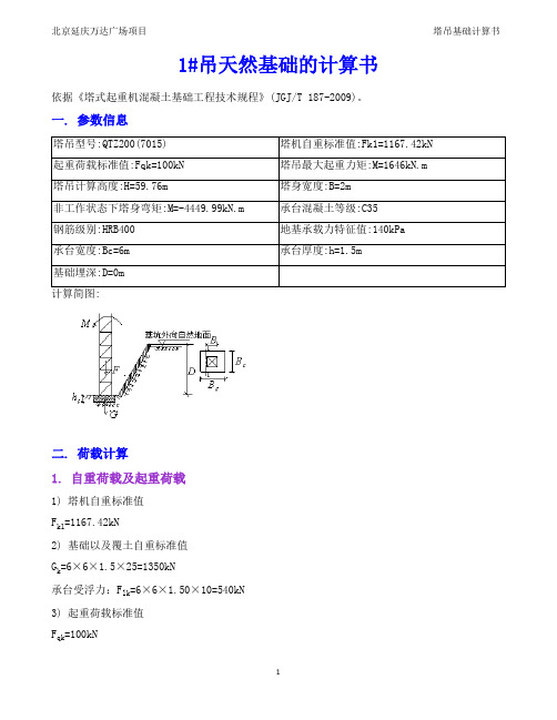
1#吊天然基础的计算书依据《塔式起重机混凝土基础工程技术规程》(JGJ/T 187-2009)。
一. 参数信息二. 荷载计算1. 自重荷载及起重荷载1) 塔机自重标准值F k1=1167.42kN2) 基础以及覆土自重标准值G k=6×6×1.5×25=1350kN承台受浮力:F lk=6×6×1.50×10=540kN3) 起重荷载标准值F qk=100kN2. 风荷载计算1) 工作状态下塔机塔身截面对角线方向所受风荷载标准值a. 塔机所受风均布线荷载标准值 (Wo=0.2kN/m2)=0.8×1.59×1.95×1.4876×0.2=0.74kN/m2=1.2×0.74×0.35×2=0.62kN/mb. 塔机所受风荷载水平合力标准值F vk =qsk×H=0.62×59.76=37.04kNc. 基础顶面风荷载产生的力矩标准值M sk=0.5F vk×H=0.5×37.04×59.76=1106.90kN.m2) 非工作状态下塔机塔身截面对角线方向所受风荷载标准值a. 塔机所受风均布线荷载标准值 (本地区 Wo=0.30kN/m2)=0.8×1.62×1.95×1.4876×0.3=1.13kN/m2=1.2×1.13×0.35×2=0.95kN/mb. 塔机所受风荷载水平合力标准值F vk=q sk×H=0.95×59.76=56.62kNc. 基础顶面风荷载产生的力矩标准值M sk=0.5F vk×H=0.5×56.62×59.76=1691.68kN.m3. 塔机的倾覆力矩工作状态下,标准组合的倾覆力矩标准值M k=-4449.99+0.9×(1646+1106.90)=-1972.38kN.m非工作状态下,标准组合的倾覆力矩标准值M k=-4449.99+1691.68=-2758.31kN.m三. 地基承载力计算依据《塔式起重机混凝土基础工程技术规程》(JGJ/T 187-2009)第4.1.3条承载力计算。
003产品审核--检验规程
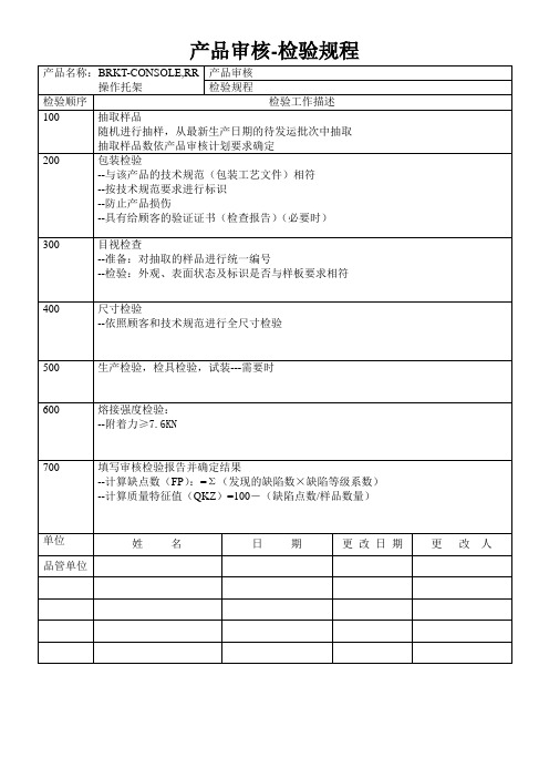
更改人
品管单位
300
目视检查
--准备:对抽取的样品进行统一编号
--检验:外观、表面状态及标识是否与样板要求相符
400
尺寸检验
--依照顾客和技术规范进行全尺寸检验
500
生产检验,检具检验,试装---需要时
600
熔接强度检验:
--附着力≥7.6KN
700
填写审核检验报告并确定结果
--计算缺点数(FP):=Σ(发现的缺陷数×缺陷等级系数)
产品审核-检验规程
产品名称:BRKT-CONSOLE,RR操作托架
产品审核
检验规程
检验顺序
检验工作描述
100
抽取样品
随机进行抽样,从最新生产日期的待发运批次中抽取
抽取样品数依产品审核计划要求确定
200
包装检验
--与该产品的技术规范(包装工艺文件)相符
--按技术规范要求进行标识
--防止产品损伤
--具有给顾客的验证证书(检查报告)(必要时)
纸张开本幅面尺寸表
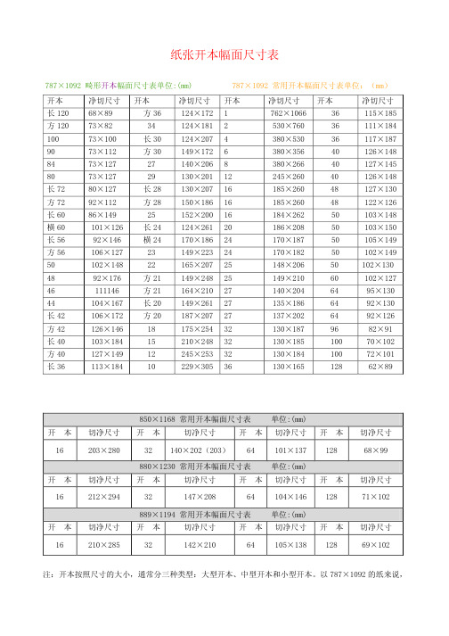
98×26 101×27 201×07 19×28 621×29 031×29 031×59 721×201 031×201 941×201 941×501 051×301 841×301 621×221 031×721 841×621 541×721 841×621 781×711 481×111 581×511 寸尺切净
mm08 x mm582 x mm004:寸尺准标 �袋提手 mm083 x mm045 开 4 mm562 x mm673 开 8:寸尺准标 �旗挂 mm083 x mm045:寸尺准标 �画贴招 mm503 x mm022:寸尺准标 �套封件文 mm582 x mm012)4A( :寸尺准标 �册传宣通普 mm582 x mm012)4A( :寸尺准标 �告广页折三
MM45x58 �卡 CI mm59*09 mm09*09:版方 >角圆<mm58*45 >角方<mm09*05:版竖 >角圆<mm45*58 >角方<mm55*09:版横 �片名 041 x 302 开 23 031 x 481 开 23 582 x 012 开 61 062×581 开 61 024 x 582 开8 073×062 开8 075 x 024 开4 045×073
821 001 001 69 46 46 46 06 05 05 05 05 05 84 84 04 04 04 63 63 63 本开
561×031 481×031 581×031 781×031 202×731 681×531 402×041 012×941 602×841 281×071 781×071 802×681 262×481 062×581 062×581 062×542 662×083 653×083 035×083 067×035 6601×267 寸尺切净
《一般管理学原理》(第四版) 003 一般管理学原理(第四版)第三章

但是,公平与效率之间又是矛盾着的,当人们突出了公平的原 则时,效率就可能出现下降的趋势;反过来,当人们把视线放在提 高效率上的时候,公平的问题也就可能表现出来。
一般管理学原理(第四版)
新编21世纪公共管理系列教材
从行为科学的角度对组织的内涵进行了揭示。 在管理实践中,组织的作用和效能就在于能够使各种资源形成
和产生密切的配合与协同作用,尤其在人力资源方面,使组织具有 单个或部分资源组合所没有的能量和功能。
组织内部成员和部门之间可以形成三种基本的工作关系,即竞 争关系、合作关系和独立关系,以及由上述三种基本关系组合而成
知识经济中的关键要素包括科学技术和管理科学两个方面,或 者说,科学技术和管理科学是推动社会发展的“两个轮子”。
对于现代管理来说,效率的理念显得越来越重要,一个合格的 管理者必须用效率理念来指导自己的管理活动。
一般管理学原理(第四版)
新编21世纪公共管理系列教材
第三章 管理的理念与原则
3.1.3 效率理念
一般管理学原理(第四版)
新编21世纪公共管理系列教材
第三章 管理的理念与原则
3.1.2 合作理念
1.合作理念的概念
合理理念是一种古老而又全新的理念。对于现代管理来说,合 作理念是最基本的管理理念之一,它是一种存在于组织之中的有利
于协调组织行为、增强组织凝聚力和提高组织绩效的团队精神。 早在20世纪50年代中期,巴纳德就提出了“协作系统”的概念,
以完善,需从以下几个方面着手: 5 加强沟通协商,树立合作意识。 6 利益平衡与目标导向相结合。 7 评价合作意愿,优化合作组合。
一般管理学原理(第四版)
中国电子展 展商名单
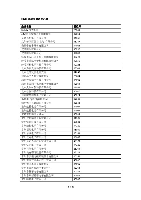
宁波福特继电器有限公司
2D067
宁波高胜电子有限公司
2C089
宁波和高磁电技术有限公司
3B245
宁波华宇电子有限公司
3C224
宁波汇龙仓电子有限公司
2D186
宁波佳和壳体有限公司
3A184
宁波嘉林电子有限公司
4C229
宁波科发电子有限公司
2C121
宁波三和壳体有限公司
3A187
宁波市北仑大矸飞达电器厂
慈溪市大发连接器厂
2C169
慈溪市宏晟机械设备有限公司
4A172
慈溪市鸿义电器实业有限公司
3B184
慈溪市骅杰电子有限公司
2D247
慈溪市杰科电子有限公司
2D204
慈溪市凯峰电子有限公司
2C201
慈溪市万捷电子有限公司
4C201
慈溪逍林创翔电子厂
3C209
慈溪中益电子器材厂
2D187
达任胶粘剂(南京)有限公司
广州市百庄复合材料有限公司
3B226
广州市创裕五金工具商行
3A048
广州市多一电子有限公司
3A003
广州市宏诚集业电子科技有限公司
3B089
广州市三堡电子技术有限公司
3B129
广州市索尔半导体有限公司
4B169
广州市太和电路板有限公司
2B084
广州泰亨电子电器有限公司
4C186
贵州航天电器股份有限公司
4B046
上海弘名电子有限公司(台湾亿光专业授权经销商)
4A041
上海华测先越材料技术有限公司
4A261
上海惠群电子有限公司
2D291
上海金嘉乐空气技术有限公司
- 1、下载文档前请自行甄别文档内容的完整性,平台不提供额外的编辑、内容补充、找答案等附加服务。
- 2、"仅部分预览"的文档,不可在线预览部分如存在完整性等问题,可反馈申请退款(可完整预览的文档不适用该条件!)。
- 3、如文档侵犯您的权益,请联系客服反馈,我们会尽快为您处理(人工客服工作时间:9:00-18:30)。
四年级英语练习(4A003)
Class_______________ Name _____________ 一、写短语
这只老虎那只狮子
你的猫他的狗
她的圆珠笔我的铅笔
给你。
谢谢你。
二、写出下列词语的缩略形式
what is that is
is not it is
三、当个小小翻译家
1. 这是一只猴子。
那是一只熊。
2. ----这是什么?----它是一把尺子。
3. ----那是什么?----是橡皮。
4. ----我认为那是她的笔记本。
----不,不是的。
5. ----我可以为苏阳拿一个书签吗?----好的,给你。
6. ----这里有给你的一个笔袋。
----谢谢。
7. ----这只熊猫是给你的。
----谢谢。
8. ----那只兔子是给高山的。
----好的。
四、在句子中的错误下方划线,并将正确的内容写在括号里
1. This’s an apple, I think. ()
2. That’s you toy panda. ()
3. What’s this? Is a monkey. ()
4. May I have pen ? ()
5. May I have that pencil case is for David? ()
6. That blue bike for Nancy. ()
7. The pen and that pencil is for you. ()
8. Here’s a ruler is for you. ()
9. This is her a lion, I think. ()
10. That a school bag is red. ()
五、根据上下文将对话补充完整
A: __________ I come__________ ?
B: __________. __________ __________, please.
A: What __________ nice room!
B: Thank __________.
A: __________ that on your desk?
B: __________ a box.
A: __________ in the box?
B: My toys.
A: Can I have a look __________ your toys?
B: Sure. Le t’s go and see.
A: __________ is this?
B: __________ is a tiger.
A: This is your panda, I think.
B: No, it __________. __________ my bear.
A: You have got many (许多)dogs. May I __________ a white one? I like __________.
B: Sure. This white dog __________ __________ __________.
A: __________.
六、朗读一、二两个单元的所有内容20分钟。
将所学的单词再背诵一遍。
你做到了吗?。