ESRH181M02R中文资料
铁氧体参数及国内外牌号对照表
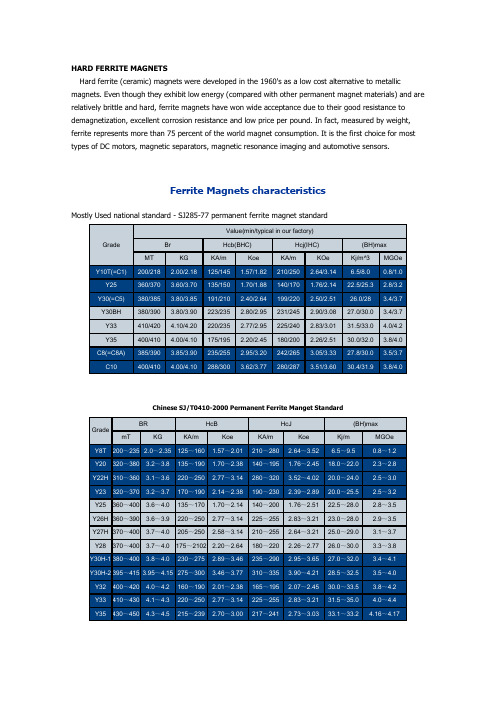
HARD FERRITE MAGNETSHard ferrite (ceramic) magnets were developed in the 1960's as a low cost alternative to metallic magnets. Even though they exhibit low energy (compared with other permanent magnet materials) and are relatively brittle and hard, ferrite magnets have won wide acceptance due to their good resistance to demagnetization, excellent corrosion resistance and low price per pound. In fact, measured by weight, ferrite represents more than 75 percent of the world magnet consumption. It is the first choice for most types of DC motors, magnetic separators, magnetic resonance imaging and automotive sensors.Ferrite Magnets characteristicsMostly Used national standard - SJ285-77 permanent ferrite magnet standardChinese SJ/T0410-2000 Permanent Ferrite Manget StandardIn MMPA(0100-87) standardRing shape size(mm) D×d×HФ115×45×5~23 Ф200×86×5~27 Ф70×32×3~17 Ф115×43×5~23 Ф200×83×5~27 Ф70×30.5×3~17 Ф115×45×5~23 Ф200×86×5~27 Ф70×32×3~17 Ф115×57×5~23 Ф200×95×5~27 Ф70×56×3~17 Ф115×58.7×3~23Ф200×100×5~27 Ф70×40×3~17 (elliptical)Ф115×60×5~23 Ф200×110×5~27 Ф71×40×3~17 Ф115×67×5~23 Ф200×120×5~27 Ф71×30.5×3~17 Ф115×80×5~23 Ф206×88.9×5~30 Ф71×32×3~17 Ф121×45×5~24 Ф206×89×5~30 Ф72×30.5×3~16 Ф121×57×5~24 Ф206×118×5~30 Ф72×32×3~16 Ф121×60×5~24 Ф210×86×5~30 Ф72×38×3~16 Ф121×65×5~24 Ф210×118×5~30 Ф72×40×3~16NdFeBKnown as third generation of Rare Earth magnets, Neodymium Iron Boron (NdFeB) magnets are the most powerful and advanced commercialized permanent magnet today. Since they are made from Neodymium, one of the most plentiful rare earth elements, and inexpensive iron, NdFeB magnets offer the best value in cost and performance.NdFeB magnets are available in both sintered and bonded forms. Sintered NdFeB offers the highest magnetic properties (28 MGOe to 50 MGOe) while Bonded NdFeB offers lower energy properties. Although bonded magnets do not possess magnetic properties as advanced as those of sintered magnets, they can be made in shapes and sizes that are difficult to achieve with sintering.A variety of coatings can be applied to the magnets' surface to overcome the principle drawback of neodymium-based magnets, their tendency to corrode easily.Grade Max. EnergyProductRemanence Coercive Force Rev. Temp.Coeff.CurieTemp.WorkingTemp. (BH)max B r H c H ci B d H d T c T w MGOe kJ/m3kG mT kOe kA/m kOe kA/m%/°C%/°C°C°CN3331-33247-26311.30-11.701130-1170>10.5>836>12>955-0.12-0.6031080 N3533-36263-28711.70-12.101170-1210>10.9>868>12>955-0.12-0.60310801.Licensed Products by SSMC-MQ - ISO 9002 Quality Standard Certified2.The above-mentioned data of magnetic parameters and physical properties are given at room temperature.3.The maximum service temperature of magnet is changeable due to the ratio length and diameter and enviromental factors.4.Special properties can be achieved with custom method.Physical and Mechanical PropertiesMax Working Temperature。
RE22R2AMR产品数据手册说明书

RE22R2AMR.T h e i n f o r m a t i o n p r o v i d e d i n t h i s d o c u m e n t a t i o n c o n t a i n s g e n e r a l d e s c r i p t i o n s a n d /o r t e c h n i c a l c h a r a c t e r i s t i c s o f t h e p e r f o r m a n c e o f t h e p r o d u c t s c o n t a i n e d h e r e i n .T h i s d o c u m e n t a t i o n i s n o t i n t e n d e d a s a s u b s t i t u t e f o r a n d i s n o t t o b e u s e d f o r d e t e r m i n i n g s u i t a b i l i t y o r r e l i a b i l i t y o f t h e s e p r o d u c t s f o r s p e c i f i c u s e r a p p l i c a t i o n s .I t i s t h e d u t y o f a n y s u c h u s e r o r i n t e g r a t o r t o p e r f o r m t h e a p p r o p r i a t e a n d c o m p l e t e r i s k a n a l y s i s , e v a l u a t i o n a n d t e s t i n g o f t h e p r o d u c t s w i t h r e s p e c t t o t h e r e l e v a n t s p e c i f i c a p p l i c a t i o n o r u s e t h e r e o f .N e i t h e r S c h n e i d e r E l e c t r i c I n d u s t r i e s S A S n o r a n y o f i t s a f f i l i a t e s o r s u b s i d i a r i e s s h a l l b e r e s p o n s i b l e o r l i a b l e f o r m i s u s e o f t h e i n f o r m a t i o n c o n t a i n e d h e r e i n .Product data sheetCharacteristicsRE22R2AMROn-delay Timing Relay - 0.05s…300h - 24…240V AC/DC - 2C/OMainRange of product Zelio TimeProduct or component typeModular timing relay Discrete output type Relay Device short name RE22Nominal output current8 AComplementaryContacts type and composition 1 C/O timed or instantaneous contact, cadmium free 1 C/O timed contact, cadmium free Time delay type A AwTime delay range0.3...3 s 1...10 s 0.05...1 s 3...30 s 10...100 s 30...300 s 3...30 min 30...300 min 3...30 h 30...300 hControl typeExternal potentiometer Diagnostic button Rotary knob[Us] rated supply voltage 24...240 V AC/DC at 50/60 Hz Release input voltage <= 2.4 V Voltage range 0.85...1.1 Us Supply frequency 50...60 Hz (+/- 5 %)Connections - terminalsScrew terminals : 2 x 0.2...2 x 1.5 mm², AWG 24...AWG 16 flexible cable with ca-ble endScrew terminals : 1 x 0.2...1 x 2.5 mm², AWG 24...AWG 14 flexible cable with ca-ble endScrew terminals : 2 x 0.5...2 x 2.5 mm², AWG 20...AWG 14 solid cable without cable endScrew terminals : 1 x 0.5...1 x 3.3 mm², AWG 20...AWG 12 solid cable without cable endTightening torque 0.6...1 N.m conforming to IEC 60947-1Housing material Self-extinguishingRepeat accuracy +/- 0.5 % conforming to IEC 61812-1Temperature drift +/- 0.05 %/°C Voltage drift+/- 0.2 %/VSetting accuracy of time delay +/- 10 % of full scale at 25 °C conforming to IEC 61812-1Control signal pulse width 30 ms100 ms (with load in parallel)Insulation resistance 100 MOhm at 500 V DC conforming to IEC 60664-1Recovery time120 ms (on de-energisation)Immunity to microbreaks <= 10 ms Power consumption in VA3 VA at 240 V ACPower consumption in W 1.5 W at 240 V DCSwitching capacity in VA2000 VAMinimum switching current10 mA 5 V DCMaximum switching current8 AMaximum switching voltage250 V ACElectrical durability100000 cycles for 2 A at 24 V DC-1100000 cycles for 8 A at 250 V AC-1Mechanical durability10000000 cyclesRated impulse withstand voltage 5 kV for 1.2...50 µs conforming to IEC 60664-1Power on delay< 100 msCreepage distance 4 kV/3 conforming to IEC 60664-1Overvoltage category III conforming to IEC 60664-1Mounting position Any positionMounting support35 mm DIN rail conforming to EN/IEC 60715Status LED Yellow LED (slow flashing) for timing in progress and output relay energisedYellow LED (fast flashing) for timing in progress and output relay de-energisedYellow LED (steady) for output relay energisedGreen LED backlight (steady) for dial pointer indicationProduct weight0.105 kgEnvironmentDielectric strength 2.5 kV for 1 mA/1 minute at 50 Hz between relay output and power supply withbasic insulation conforming to IEC 61812-1Standards IEC 61812-1UL 508Directives2004/108/EC - electromagnetic compatibility2006/95/EC - low voltage directiveProduct certifications CCCCECSAGLULRCMEACChina RoHSAmbient air temperature for operation-20...60 °CAmbient air temperature for storage-40...70 °CIP degree of protection IP50 (front panel) conforming to IEC 60529IP20 (terminals) conforming to IEC 60529IP40 (housing) conforming to IEC 60529Pollution degree 3 conforming to IEC 60664-1Vibration resistance20 m/s² (f = 10...150 Hz) conforming to IEC 60068-2-6Shock resistance 5 gn (in operation) (duration = 11 ms) conforming to IEC 60068-2-2715 gn (not operating) (duration = 11 ms) conforming to IEC 60068-2-27 Relative humidity95 % at 25...55 °CElectromagnetic compatibility Immunity to microbreaks and voltage drops (test level: 100 % - 20 ms) conform-ing to IEC 61000-4-11Immunity to microbreaks and voltage drops (test level: 30 % - 500 ms) conform-ing to IEC 61000-4-11Fast transient bursts (test level: 2 kV, level 3 - direct contact) conforming to IEC61000-4-4Conducted RF disturbances (test level: 10 V, level 3 - 0.15...80 MHz) conformingto IEC 61000-4-6Radiated radio-frequency electromagnetic field immunity test (test level: 10 V/m,level 3 - 80 MHz...1 GHz) conforming to IEC 61000-4-3Electrostatic discharge (test level: 8 kV, level 3 - air discharge) conforming to IEC61000-4-2Electrostatic discharge (test level: 6 kV, level 3 - contact discharge) conforming toIEC 61000-4-2Surge immunity test (test level: 2 kV, level 3 - common mode) conforming to IEC61000-4-5Surge immunity test (test level: 1 kV, level 3 - differential mode) conforming toIEC 61000-4-5Fast transients immunity test (test level: 1 kV, level 3 - capacitive connecting clip)conforming to IEC 61000-4-4Product data sheetRE22R2AMR Dimensions DrawingsDimensionsProduct data sheetRE22R2AMR Connections and SchemaWiring DiagramProduct data sheetRE22R2AMRTechnical DescriptionFunction A: Power On-DelayDescriptionOn energisation of power supply, the timing period T starts. After timing, the output(s) R close(s).The second output (R2) can be either timed (when set to "TIMED") or instantaneous (when set to "INST").Function: 1 OutputFunction: 2 OutputsFunction Aw : Power On-Delay With Retrigger / Restart ControlDescriptionOn energisation of power supply, the timing period T starts.At the end of the timing period T, the output(s) R close(s).Energization of Y1 makes the output(s) R open(s).Deenergization of Y1 restarts timing period T.At the end of timing period T, the output(s) R close(s).The second output (R2) can be either timed (when set to "TIMED") or instantaneous (when set to "INST")Function: 1 OutputFunction: 2 OutputsLegendRelay de-energisedRelay energisedOutput openOutput closedUSupply-TTiming period-R1/2 timed outputsR2-R2The second output is instantaneous if the right position is selected inst.-Retrigger / Restart controlY1-RE22R2AMR.。
ESRH资料

CDE Cornell Dubilier • 1605 E. Rodney French Blvd. • New Bedford, MA 02744 • Phone: (508)996-8561 • Fax: (508)996-3830 • Type ESRHSolid Polymer Aluminum SMT CapacitorsSolid P olymer A luminum capacitors are now available with a +125ºC temperature rating. CDE’s type ESRH capacitors are rated at +125ºC for 1000 hours when operated at 3/4 of the 105ºC rated voltage. Solid Polymer Aluminum electrolytic capacitors feature extremely low ESR which yields a capacitor with very low high frequency impedance and high ripple current capability. When low ESR is your requirement, one type ESRH capacitor can replace three or more tantalum or aluminum electrolytic capacitors. The solid electrolyte in a polymer aluminum capacitor results in a long (and ignition free) life, and the 7.3 x 4.3 footprint is compatible with “D” case solid tantalum capacitors.SpecificationsMarkingsOperating Temperature Range:Capacitance Tolerance:Dissipation Factor (DF):Surge Voltage:DC Leakage Current (after 2 minutes):-55 ºC to +105 ºC at rated voltage (+125 ºC at .75 x rated voltage)±20% at 120 Hz and +20 ºC ≤0.10 at 120 Hz and +20 ºC 1.25 x rated voltage I ≤ .1 CVESRH101M08RPackaging CodeCDE TypeCapacitanceCode Capacitance Tolerance WVDC CodeR = Tape & Reel 2000 pcs/reel02 =2.0 Vdc 06 = 6.3 Vdc 680 = 68 µF M = ±20%0E =2.5 Vdc 08 = 8.0 Vdc101 = 100 µF04 =4.0 VdcLot CodeCapacitance(“R” = Decimal Point)元器件交易网Type ESRH Solid Polymer Aluminum SMT Capacitors CDE Cornell Dubilier • 1605 E. Rodney French Blvd. • New Bedford, MA 02744 • Phone: (508)996-8561 • Fax: (508)996-3830 • Low E.S.R. and High TemperatureOutline DrawingRatings*12mm wide tape — 13” diameter reelCapacitance(µF)Rated Voltage WVDCCatalog Maximum Ripple Current Part Number E.S.R.at 100 kHz H ±0.2Tape* and Reel 100 kHz/20 ºC+20 ºC to + 125 ºC(mm)(2000 pcs/reel)(Ω)(A rms )180 2.0ESRH181M02R 0.015 2.5 2.8150 2.5ESRH151M0ER 0.015 2.5 2.8120 4.0ESRH121M04R 0.015 2.5 2.8100 6.3ESRH101M06R 0.015 2.5 2.8688.0ESRH680M08R 0.015 2.5 2.8270 2.0ESRH271M02R 0.012 3.0 4.1220 2.5ESRH221M0ER 0.012 3.0 4.1180 4.0ESRH181M04R 0.012 3.0 4.1150 6.3ESRH151M06R 0.012 3.0 4.11008.0ESRH101M08R0.0123.04.1MarkingsLand Pattern元器件交易网CDE Cornell Dubilier • 1605 E. Rodney French Blvd. • New Bedford, MA 02744 • Phone: (508)996-8561 • Fax: (508)996-3830 • Type ESRH Solid Polymer Aluminum SMT CapacitorsTypical Impedance & ESRLife Test:Apply rated DC working voltage at 105 ºC (or 0.75 x WVDC at 125 ºC) for 1000 hours, and then stabilize them to +20 ºC. Capacitors will meet the following limits:∆C = ±10% of the initial measured value DF & DCL ≤ the initial specified valueShelf Life Test:Shelf life is typically 5 to 10 years. Accelerated test:after 500 hours at125 ºC, capacitors will meet thefollowing limits after stabilization at 20 ºC: ∆C = ±10% of the initial measured value DF & DCL ≤ the initial specified valueMoisture Resistance:After 500 hours storage at +60 ºC and 90% R.H. without load, the capacitor will meet the following limits:∆C = +70%/–20% of the initial measured value (2.0 & 2.5 Vdc),+60%/–20% of the initial measured value (4.0 Vdc), +50%/–20% of the initial measured value (6.3 Vdc), +40%/–20% of the initial measured value (8.0 Vdc).DF ≤ two times the initial specified value DCL ≤ the initial specified valueResistance to Soldering Heat:Capacitors withstand being heated in an oven at 235 ºC for 200 seconds.Soldering:Solid Polymer Aluminum capacitors are designed for reflow soldering.Preheat the capacitors at 160 ºC for a maximum of120 seconds. The time at or above 200 ºC on thesurface of the capacitor should be per thefollowing chart:Frequency (kHz)ESRH271M02R 270 µF/2VImpedance/ESRESRH680M02R 680 µF/2VImpedance/ESRSpecifications (continued)(For more information on this product see the Solid Polymer Aluminum Application Guide)元器件交易网。
SY89297UMH;SY89297UMG;SY89297UMG TR;SY89297UMH TR;中文规格书,Datasheet资料
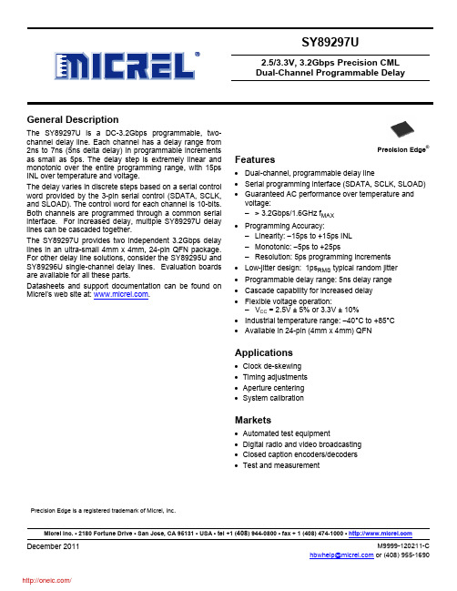
SY89297U2.5/3.3V, 3.2Gbps Precision CML Dual-Channel Programmable DelayPrecision Edge is a registered trademark of Micrel, Inc.Micrel Inc. • 2180 Fortune Drive • San Jose, CA 95131 • USA • tel +1 (408) 944-0800 • fax + 1 (408) 474-1000 •General DescriptionThe SY89297U is a DC-3.2Gbps programmable, two-channel delay line. Each channel has a delay range from 2ns to 7ns (5ns delta delay) in programmable increments as small as 5ps. The delay step is extremely linear and monotonic over the entire programming range, with 15ps INL over temperature and voltage.The delay varies in discrete steps based on a serial control word provided by the 3-pin serial control (SDATA, SCLK, and SLOAD). The control word for each channel is 10-bits. Both channels are programmed through a common serial interface. For increased delay, multiple SY89297U delay lines can be cascaded together.The SY89297U provides two independent 3.2Gbps delay lines in an ultra-small 4mm x 4mm, 24-pin QFN package. For other delay line solutions, consider the SY89295U and SY89296U single-channel delay lines. Evaluation boards are available for all these parts.Datasheets and support documentation can be found on Micrel’s web site at: .Precision Edge ®Features• Dual-channel, programmable delay line• Serial programming interface (SDATA, SCLK, SLOAD) • Guaranteed AC performance over temperature and voltage:– > 3.2Gbps/1.6GHz f MAX • Programming Accuracy: – Linearity: −15ps to +15ps INL – Monotonic: −5ps to +25ps– Resolution: 5ps programming increments • Low-jitter design: 1ps RMS typical random jitter • Programmable delay range: 5ns delay range • Cascade capability for increased delay • Flexible voltage operation:– V CC = 2.5V ± 5% or 3.3V ± 10% • Industrial temperature range: −40°C to +85°C • Available in 24-pin (4mm x 4mm) QFNApplications• Clock de-skewing • Timing adjustments • Aperture centering • System calibrationMarkets• Automated test equipment• Digital radio and video broadcasting • Closed caption encoders/decoders • Test and measurementOrdering Information(1)Part Number Package Type Operating Range Package Marking Lead FinishSY89297UMG QFN-24 Industrial 297U with Pb-Free Bar Line Indicator Pb-Free NiPdAuSY89297UMGTR(2)QFN-24 Industrial 297U with Pb-Free Bar-Line Indicator Pb-Free NiPdAuNotes:1. Contact factory for die availability. Dice are guaranteed at T= 25°C, DC electricals only.A2. Tape and Reel.Pin Configuration24-Pin QFNTruth TablesInputs Outputs INA, INB /INA, /INB QA, QB /QA, /QB0 1 0 11 0 1 0Table 1. Inputs/Outputs/ENA, /ENB Q, /Q (A, B)1 Q = Low, /Q = HIGH0 IN, /IN Delayed (normal operation)Table 2. Input Enable (Latches Outputs)Functional Block DiagramPin DescriptionPin NumberPin Name Pin Function1 2INA /INAChannel A Differential Input: INA and /INA pins receive the Channel A data. QA and /QA are the delayed product of INA and /INA. Each input is internally terminated to VTA through a 50Ω resistor (100Ω across INA and /INA).3 VTA Input A Termination Center-Tap: Each side of the differential input pair terminates to this pin.This pin provides a center-tap to a termination network for maximum interface flexibility. See“Input Interface Applications” section. 4 VTBInput B Termination Center-Tap: Each side of the differential input pair terminates to this pin. This pin provides a center-tap to a termination network for maximum interface flexibility. See “Input Interface Applications” section. 5 6INB /INBChannel B Differential Input: INB and /INB pins receive the Channel B data. QB and /QB are the delayed product of INB and /INB. Each input is internally terminated to VTB through a 50Ω resistor (100Ω across INB and /INB).7 VREF-ACReference Voltage Output: For AC-coupled input signals, this pin can bias the inputs IN and /IN. Connect VREF-AC directly to the VT input pin for each channel. De-couple to V CC using a0.01µF capacitor. Maximum sink/source current is ±0.5mA. For DC-coupled input applications, leave VREF-AC pin floating. 8, 11, 20GND, Exposed PadNegative Supply: Exposed pad must be connected to a ground plane that is the same potential as the ground pins.9 /ENACMOS/TTL-Compatible Enable Input: When the /ENA pin is pulled HIGH, QA is held LOW and /QA goes HIGH after the programmed delay propagates through the part. /ENA contains a 67k Ω pull-down resistor and defaults LOW when left floating. Logic threshold level is V CC /2 10 /ENBCMOS/TTL-Compatible Enable Input: When the /ENB pin is pulled HIGH, QB is held LOW and /QB goes HIGH after the programmed delay propagates through the part. /ENB contains a 67k Ω pull-down resistor and defaults LOW when left floating. Logic threshold level is Vcc/2 12, 15, 16, 19VCC Power Supply: Bypass each supply pin with 0.1µF//0.01µF low-ESR capacitors. See DC Electrical Characteristics table for more details. 2.5V ±5% or 3.3V ±10%.13 14 /QB QB CML Differential Output: QB and /QB are the delayed product of INB, /INB. CML outputs are terminated at the destination with 100Ω across the pair. See “CML Output Termination” section.17 18/QA QACML Differential Output: QA and /QA are the delayed product of INA, /INA. CML outputs are terminated at the destination with 100Ω across the pair. See “CML Output Termination” section.23 22SCLK SDATACMOS/TTL-compatible 3-pin serial programming control inputs: The 3-pin serial control sets each channel’s IN to Q delay. DA(0:9) control channel A delay. DB(0:9) control channel B. To program the two channels, insert a 20-bit word (DA0:DA9 and DB0:DB9) into SDATA and clock in the control bits with SCLK. Maximum input frequency to SCLK is 40MHz. Data is loaded into the serial registers on the L-H transition of SCLK. After all 20-bits are clocked in, SLOAD latches the new delay bits. These pins have internal pull-downs at the inputs. See “ACElectrical Characteristics” for delay values. Logic threshold level is Vcc/2. SCLK and SDATA contain a 67k Ω pull-down resistor and default LOW when left floating.24 SLOADCMOS/TTL-compatible 3-pin serial programming control input: SLOAD controls the latches that transfer scanned data to the delay line. These latches are transparent when SLOAD is high. Data transfers from the latch to the delay line on a L-H transition of SLOAD. SLOAD has to transition H-L before new data is loaded in the scan chain. When SLOAD is high, the latches are transparent and SCLK cannot switch. Otherwise, new data will immediately transfer to the scan chain. Logic threshold level is Vcc/2. SLOAD contains a 67k Ω pull-down resistor and defaults LOW when left floating. 21 SOUTCMOS/TTL-compatible output: This pin is used to support cascading multiple SY89297U delay lines. Serial data is clocked into the SDATA input and is clocked out of SOUT into the next SY89297U delay line. SOUT pin includes an internal 550Ω pull-up resistor.Absolute Maximum Ratings(1)Supply Voltage (V CC) .................................. –0.5V to +4.0V Input Voltage (V IN) .......................................... –0.5V to V CC CML Output Voltage (V OUT)… ....... V CC −1.0V to V CC +0.5V Current (V T)Source or Sink Current on VT pin ..................... ±70mA Input CurrentSource or Sink Current on (IN, /IN) .................. ±35mA Current (V REF)Source or sink current on V REF-AC(2) ................ .±0.5mA Maximum operating Junction Temperature ............ 125°C Lead Temperature (soldering, 20sec.) ..................... 260°C Storage Temperature (T s) ....................... –65°C to +150°C Operating Ratings(3)Supply Voltage (V CC)T A (−40°C to +85°C) ................ +2.375V to +2.625VT A (−40°C to +75°C) .......................... +3.0V to 3.6V Ambient Temperature (T A) .......................... −40°C to +85°C Package Thermal Resistance(4)QFN (θJA)Still-Air...............................................................43°C/W QFN (ψJB)Junction-to-Board...........................................30.5°C/WDC Electrical Characteristics(5)T A = −40°C to +85°C, Channels A and B, unless otherwise stated.Symbol Parameter Condition Min. Typ. Max. UnitsV CC Power Supply Voltage Range T A: −40°C to +85°C 2.375 2.5 2.625 V T A: −40°C to +75°C 3.0 3.3 3.6 V T A: −40°C to +85°C,Airflow = 500 LFPM3.0 3.3 3.6 VI CC PowerSupplyCurrent Maximum V CC, Both ChannelsCombined, Output Load Included195 250 mAR IN Input Resistance(IN-to-VT, /IN-to-VT)455055ΩR DIFF_IN Differential Input Resistance(IN-to-/IN)90100110ΩV IH Input HIGH Voltage (IN, /IN) 1.2 V CC V V IL Input LOW Voltage (IN, /IN) 0 V IH–0.1 V V IN Input Voltage Swing (IN, /IN) See Figure 5a 0.1 1.0 VV DIFF_IN Differential Input Voltage Swing(|IN - /IN|)See Figure 5b 0.2 VV REF-AC Output Reference Voltage V CC–1.3 V CC–1.2 V CC–1.1 VV T_IN Voltage from Input to V T 1.28 V Notes:1. Permanent device damage may occur if “Absolute Maximum Ratings” are exceeded. This is a stress rating only and functional operation is notimplied at conditions other than those detailed in the operational sections of this data sheet. Exposure to “Absolute Maximum Rating” conditions for extendedperiodsmayaffectdevicereliability.2. Due to the limited drive capability, use for input of the same package only.3. The data sheet limits are not guaranteed if the device is operated beyond the operating ratings.4. Thermal performance on QFN packages assumes exposed pad is soldered (or equivalent) to the device most negative potential (GND).5. The circuit is designed to meet the DC specifications shown in the table after thermal equilibrium has been established.CML Outputs DC Electrical Characteristics (6)V CC = +2.5V +5% or +3.3V ±10%, R L = 100Ω across the outputs; T A = −40°C to +85°C, unless otherwise stated. Symbol Parameter Condition Min. Typ. Max. Units V OH Output HIGH Voltage R L = 50Ω to V CC V CC −0.020 V CC −0.010V CC VV OUT Output Voltage SwingSee Figure 5a 325 400 mV V DIFF_OUTDifferential Output Voltage SwingSee Figure 5b650 800 mV R OUT Output Source Impedance455055ΩLVTTL/CMOS DC Electrical Characteristics (6)V CC = +2.5V +5% or 3.3V ±10%, T A = −40°C to +85°C, unless otherwise stated. Symbol Parameter Condition Min. Typ. Max. Units V IH Input HIGH Voltage 2.0 V V IL Input LOW Voltage0.8 V I IH Input HIGH Current V IH = VCC 150 µA I IL Input LOW Current V IL = 0.8V50µAV OLOutput LOW Voltage SOUT Pin; I OL =1mA 0.55 VOutput High Leakage CurrentSOUT = V CC 100 µANote:6. The circuit is designed to meet the DC specifications shown in the above table after thermal equilibrium has been established.AC Electrical Characteristics (7)T A = −40°C to +85°C, Channels A and B, unless otherwise stated. Symbol Parameter ConditionMin. Typ. Max. Units f MAXMaximum Operating FrequencyClock: V out Swing >200mV pk 1.6 GHzNRZ Data3.2Gbpst pdPropagation Delay IN to Q; D[0–9]=0 IN to Q; D[0–9]=1023/EN to Q: D[0–9]=0; V TH = V CC /2 SDATA to SOUT (D0–D9=Low), No load1000 5500 1000 20002000 7500 2500 4500pst RANGE Programmable Ranget pd (max) – t pd (min)4150 5115 pst SKEWDuty Cycle Skew t PHL – t PLH Note 84555%AC Electrical Characteristics(7)T A = −40°C to +85°C, Channels A and B, unless otherwise stated.Symbol Parameter Condition Min. Typ. Max. UnitsΔt Step DelayD0 HighD1 HighD2 HighD3 HighD4 HighD5 HighD6 HighD7 HighD8 HighD9 HighD0-D9 High510204080160320640128025605115ps Monotonic −5 25INL IntegralNon-Linearity Note 9 −15 +15 pst S Setup TimeSDATA to SCLKSCLK to SLOAD/EN to INNote 10Note 11400400300pst H Hold TimeSLOAD to SCLKIN to /ENSCLK to SDATANote 12Note 13300−100200pst PW Pulse Width SLOAD 1000 ps t R Release Time /EN to IN Note 14 800 pst JITTER Cycle-to-Cycle JitterTotal JitterRandom JitterNote 15Note 16Note 172202ps RMSps PPps RMSt r, t f Output Rise/Fall Time 20% to 80% (Q) 30 55 80 ps Duty Cycle Input Frequency = 1.6GHz 45 55 % Notes:7. High frequency AC electricals are guaranteed by design and characterization.8. Duty cycle skew guaranteed only for differential operation measured from the cross point of the input to the crosspoint of the output.9. INL (Integral Non-Linearity) is defined from its corresponding point on the ideal delay versus D[9:0] curve as the deviation from its ideal delay. Themaximum difference is the INL. Theoretical Ideal Linearity (TIL) = (measured maximum delay – measured minimum delay) ÷ 1023. INL = measured delay – (measured minimum delay + (step number x TIL)).10. SCLK has to transition L-H a setup time before the SLOAD H-L transition to ensure the valid data is properly latched. See timing diagram "Setupand Hold Time: SCLK and SLOAD.”11. This setup time is the minimum time that /EN must be asserted prior to the next transition of IN / /IN to prevent an output response greater than±75 mV to that IN or /IN transition. See timing diagram Setup, Hold and Release Time: IN and /EN."12. SCLK has to transition L-H a hold time after the SLOAD H-L transition to ensure that the valid data is properly latched before starting to load newdata. See timing diagram "Setup and Hold Time: SCLK and SLOAD.”13. This hold time is the minimum time that /EN must remain asserted after a negative going transition of IN to prevent an output response greater than+75mv to the IN transition. See timing diagram “Setup, Hold, and Release Time: IN and /EN.”14. This release time is the minimum time that /EN must be de-asserted prior to the next IN / /IN transition to affect the propagation delay of IN to Qless than 1ps. See timing diagram “Setup, Hold, and Release Time: IN and /EN.”15. Cycle-to-cycle jitter definition: The variation of periods between adjacent cycles over a random sample of adjacent cycle pairs.T jitter_cc = T n – T n+1, where T is the time between rising edges of the output signal.16. Total jitter definition: With an ideal clock input, no more than one output edge in 1012 output edges will deviate by more than the specified peak-to-peak jitter value.17. Random jitter definition: Jitter that is characterized by a Gaussian distribution, unbounded and is quantified by its standard deviation and mean.Random jitter is measured with a K28.7 comma defect pattern, measured at 1.5Gbps.Timing DiagramsFigure 1. Setup and Hold Time: SDATA and SCLKFigure 2. Setup and Hold Time: SCLK and SLOADTiming Diagrams (Continued)Figure 3. Set-Up, Hold, and Release Time: IN and /ENFigure 4. SLOAD Pulse Width (TPW)Typical Operating CharacteristicsV CC = +2.5V, GND = 0V, V IN = 100mV, R L = 100Ω across the outputs, T A = 25°C.Phase Noise ChartV CC = +2.5V, GND = 0V, V IN = 100mV, R L = 100Ω across the outputs, T A = 25°C.f C: 1GHz Delay Setting: 00001 00110 (2ns)分销商库存信息:MICRELSY89297UMH SY89297UMG SY89297UMG TR SY89297UMH TR。
松下ECA1HM2R2数据表说明书

Aluminum Electrolytic Capacitors/ MDesign, and specifications are each subject to change without notice. Ask factory for the current technical specifications before purchaseand / or use. Should a safety concern arise regarding this product,please be sure to contact us immediately. Mar.2006Aluminum Electrolytic Capacitors/ MDesign, and specifications are each subject to change without notice. Ask factory for the current technical specifications before purchase and / or use. Should a safety concern arise regarding this product,please be sure to contact us immediately. Mar.2006n Standard ProductsWhen requesting taped product, please put the letter "B" or "i" between the "( )". Lead wire pitch B=5mm, 7.5mm,i=2.5mm.The taping dimensions are explained on p.196 of our Catalog. Please use it as a reference guide.Endurance : 85°C 2000h(m m )(m m )(m m )(pcs)(pcs)(µF)(m m )(m m )(mm)(m A )(V)tan δ(120Hz)(+20°C)6.31025i B i i Lead Space Part No.Specification Dia.LengthTapingCase size Cap.(±20%)Lead Dia.W.V.Straight Min. Packaging Q’tyTapingTaping (+85°C)Lead LengthStraight Leads2205112400.280.5 2.0 5.0 2.5ECA0JM221( )2002000470 6.311.23800.280.5 2.5 5.0 2.5ECA0JM471( )20020001000811.55800.280.6 3.5 5.0ECA0JM102( )2001000220010168900.300.6 5.0 5.0ECA0JM222( )2005003300102010200.320.6 5.0 5.0ECA0JM332( )200500470012.52011700.340.6 5.0 5.0ECA0JM472( )200500680012.52512700.380.6 5.0 5.0ECA0JM682( )20050010000162514500.460.87.57.5ECA0JM103( )100250150001631.517000.560.87.5ECA0JM153100220001835.519000.700.87.5ECA0JM22350330 6.311.23300.240.5 2.5 5.0 2.5ECA1AM331( )200200010001012.56300.240.6 5.0 5.0ECA1AM102( )200500220010209200.260.6 5.0 5.0ECA1AM222( )200500330012.52010900.280.6 5.0 5.0ECA1AM332( )200500470012.52512000.300.6 5.0 5.0ECA1AM472( )2005006800162514000.340.87.57.5ECA1AM682( )100250100001631.516000.420.87.5ECA1AM103100150001835.518500.520.87.5ECA1AM1535010511300.200.5 2.0 5.0 2.5ECA1CM100( )200200022511750.200.5 2.0 5.0 2.5ECA1CM220( )2002000335111100.200.5 2.0 5.0 2.5ECA1CM330( )2002000475111300.200.5 2.0 5.0 2.5ECA1CM470( )20020001005111800.200.5 2.0 5.0 2.5ECA1CM101( )20020002206.311.22800.200.5 2.5 5.0 2.5ECA1CM221( )200200016470811.54400.200.6 3.5 5.0ECA1CM471( )2001000100010166800.200.6 5.0 5.0ECA1CM102( )200500220012.52010000.220.6 5.0 5.0ECA1CM222( )200500330012.52512000.240.6 5.0 5.0ECA1CM332( )2005004700162513600.260.87.57.5ECA1CM472( )10025068001631.516000.300.87.5ECA1CM682100100001835.518000.380.87.5ECA1CM10350100 6.311.21800.160.5 2.5 5.0 2.5ECA1EM101( )2002000330811.53900.160.6 3.5 5.0ECA1EM331( )20010004701012.54800.160.6 5.0 5.0ECA1EM471( )200500100010208500.160.6 5.0 5.0ECA1EM102( )200500220012.52512000.180.6 5.0 5.0ECA1EM222( )2005003300162513000.200.87.57.5ECA1EM332( )10025047001631.515000.220.87.5ECA1EM47210068001835.517500.260.87.5ECA1EM68250475111300.140.5 2.0 5.0 2.5ECA1VM470( )2002000 35100 6.311.22100.140.5 2.5 5.0 2.5ECA1VM101( )2002000220811.53500.140.63.55.0ECA1VM221( )2001000Ripple current (120Hz)Aluminum Electrolytic Capacitors/ MDesign, and specifications are each subject to change without notice. Ask factory for the current technical specifications before purchase and / or use. Should a safety concern arise regarding this product,please be sure to contact us immediately. Mar.2006n Standard ProductsWhen requesting taped product, please put the letter "B" or "i" between the "( )". Lead wire pitch B=5mm, 7.5mm,i=2.5mm.The taping dimensions are explained on p.196 of our Catalog. Please use it as a reference guide.Endurance : 85°C 2000h3563(m m )(m m )(m m )(pcs)(pcs)(µF)(m m )(m m )(mm)(m A )(V)i Bi i Lead Space Part No.SpecificationDia.LengthTapingCase sizeCap.(±20%)Lead Dia.W.V.Straight Taping Taping Ripple current(120Hz)(+85°C)Lead LengthStraightLeads3301012.54400.140.6 5.0 5.0ECA1VM331( )20050047010165500.140.6 5.0 5.0ECA1VM471( )200500100012.5209000.140.6 5.0 5.0ECA1VM102( )2005002200162512500.160.87.57.5ECA1VM222( )10025033001631.514000.180.87.5ECA1VM33210047001835.516000.200.87.5ECA1VM472500.1511 1.30.120.5 2.0 5.0 2.5ECA1HM0R1( )20020000.22511 2.90.120.5 2.0 5.0 2.5ECA1HMR22( )20020000.33511 4.40.120.5 2.0 5.0 2.5ECA1HMR33( )20020000.4751150.120.5 2.0 5.0 2.5ECA1HMR47( )20020001511100.120.5 2.0 5.0 2.5ECA1HM010( )20020002.2511200.120.5 2.0 5.0 2.5ECA1HM2R2( )20020003.3511350.120.5 2.0 5.0 2.5ECA1HM3R3( )20020004.7511450.120.5 2.0 5.0 2.5ECA1HM4R7( )200200010511650.120.5 2.0 5.0 2.5ECA1HM100( )2002000 50225111000.120.5 2.0 5.0 2.5ECA1HM220( )2002000335111100.120.5 2.0 5.0 2.5ECA1HM330( )200200047 6.311.21300.120.5 2.5 5.0 2.5ECA1HM470( )2002000100811.52500.120.6 3.5 5.0ECA1HM101( )20010002201012.54000.120.6 5.0 5.0ECA1HM221( )20050033010165000.120.6 5.0 5.0ECA1HM331( )20050047010206500.120.6 5.0 5.0ECA1HM471( )200500100012.52510500.120.6 5.0 5.0ECA1HM102( )20050022001631.513000.140.87.5ECA1HM22210033001835.515000.160.87.5ECA1HM3325010511700.110.5 2.0 5.0 2.5ECA1JM100( )2002000225111050.110.5 2.0 5.0 2.5ECA1JM220( )200200033 6.311.21300.110.5 2.5 5.0 2.5ECA1JM330( )200200047 6.311.21600.110.5 2.5 5.0 2.5ECA1JM470( )2002000100811.52700.110.6 3.5 5.0ECA1JM101( )200100022010164500.110.6 5.0 5.0ECA1JM221( )20050033010205500.110.6 5.0 5.0ECA1JM331( )20050047012.5207500.110.6 5.0 5.0ECA1JM471( )2005001000162511000.110.87.57.5ECA1JM102( )10025022001835.514000.130.87.5ECA1JM222500.47511100.100.5 2.0 5.0 2.5ECA2AMR47( )20020001511200.100.5 2.0 5.0 2.5ECA2AM010( )20020002.2511300.100.5 2.0 5.0 2.5ECA2AM2R2( )2002000 100 3.3511400.100.5 2.0 5.0 2.5ECA2AM3R3( )20020004.7511500.100.5 2.0 5.0 2.5ECA2AM4R7( )200200010511700.100.5 2.0 5.0 2.5ECA2AM100( )2002000226.311.21150.100.52.55.02.5ECA2AM220( )2002000tan δ(120Hz)(+20°C)Min. Packaging Q’tyAluminum Electrolytic Capacitors/ MDesign, and specifications are each subject to change without notice. Ask factory for the current technical specifications before purchase and / or use. Should a safety concern arise regarding this product,please be sure to contact us immediately. Mar.2006160250350n Standard ProductsWhen requesting taped product, please put the letter "B" or "i" between the "( )". Lead wire pitch B=5mm, 7.5mm,i=2.5mm.The taping dimensions are explained on p.196 of our Catalog. Please use it as a reference guide.Endurance : 85°C 2000h(m m )(m m )(m m )(pcs)(pcs)(µF)(m m )(m m )(mm)(m A )(V)i Bi i Lead Space Part No.SpecificationDia.Length TapingCase sizeCap.(±20%)Lead Dia.W.V.Straight Min. Packaging Q ’tyTaping Taping Ripple current(120Hz)(+85°C)Lead LengthStraightLeads33811.51450.100.6 3.5 5.0ECA2AM330( )200100047811.51800.100.6 3.5 5.0ECA2AM470( )200100010010163500.100.6 5.0 5.0ECA2AM101( )200500 10022012.5205500.100.6 5.0 5.0ECA2AM221( )20050033012.5257000.100.6 5.0 5.0ECA2AM331( )20050047016259000.100.87.57.5ECA2AM471( )10025010001835.513000.100.87.5ECA2AM102501 6.311.2360.160.5 2.5 5.0 2.5ECA2CM010( )20020002.2 6.311.2530.160.5 2.5 5.0 2.5ECA2CM2R2( )20020003.3 6.311.2660.160.5 2.5 5.0 2.5ECA2CM3R3( )20020004.7 6.311.2780.160.5 2.5 5.0 2.5ECA2CM4R7( )2002000101012.51050.160.6 5.0 5.0ECA2CM100( )2005002210161750.160.6 5.0 5.0ECA2CM220( )2005003310202350.160.6 5.0 5.0ECA2CM330( )2005004712.5203200.160.6 5.0 5.0ECA2CM470( )20050010012.5255150.160.6 5.0 5.0ECA2CM101( )2005002201631.58300.160.87.5ECA2CM2211003301831.510900.160.87.5ECA2CM33150470184014400.160.87.5ECA2CM471501 6.311.2340.180.5 2.5 5.0 2.5ECA2DM010( )20020002.2 6.311.2500.180.5 2.5 5.0 2.5ECA2DM2R2( )20020003.3 6.311.2620.180.5 2.5 5.0 2.5ECA2DM3R3( )20020004.7811.5860.180.6 3.5 5.0ECA2DM4R7( )2001000101012.51000.180.6 5.0 5.0ECA2DM100( )200500 2002210201800.180.6 5.0 5.0ECA2DM220( )2005003310202200.180.6 5.0 5.0ECA2DM330( )2005004712.5203000.180.6 5.0 5.0ECA2DM470( )20050010016254750.180.87.57.5ECA2DM101( )1002502201831.58350.180.87.5ECA2DM22150330184011400.180.87.5ECA2DM331501 6.311.2340.180.5 2.5 5.0 2.5ECA2EM010( )20020002.2 6.311.2500.180.5 2.5 5.0 2.5ECA2EM2R2( )20020003.3811.5720.180.6 3.5 5.0ECA2EM3R3( )20010004.7811.5860.180.6 3.5 5.0ECA2EM4R7( )20010001010161100.180.6 5.0 5.0ECA2EM100( )2005002210201800.180.6 5.0 5.0ECA2EM220( )2005003312.5202500.180.6 5.0 5.0ECA2EM330( )2005004712.5253300.180.6 5.0 5.0ECA2EM470( )2005001001631.55300.180.87.5ECA2EM10110022018409300.180.87.5ECA2EM221501 6.311.2320.200.5 2.5 5.0 2.5ECA2VM010( )20020002.2811.5550.200.63.55.0ECA2VM2R2( )2001000tan δ(120Hz)(+20°C)Aluminum Electrolytic Capacitors/ MDesign, and specifications are each subject to change without notice. Ask factory for the current technical specifications before purchase and / or use. Should a safety concern arise regarding this product,please be sure to contact us immediately. Mar.2006n Standard ProductsWhen requesting taped product, please put the letter "B" or "i" between the "( )". Lead wire pitch B=5mm, 7.5mm,i=2.5mm The taping dimensions are explained on p.196 of our Catalog. Please use it as a reference guide.Endurance : 85°C 2000h(m m )(m m )(m m )(pcs)(pcs)(µF)(m m )(m m )(mm)(m A )(V)i Bi i Lead Space Part No.SpecificationDia.LengthTapingCase sizeCap.(±20%)Lead Dia.W.V.Straight Min. Packaging Q’tyTaping Taping Ripple current (120Hz)(+85°C)Lead LengthStraightLeads3.3811.5600.200.6 3.5 5.0ECA2VM3R3( )20010004.71012.5650.200.65.0 5.0ECA2VM4R7( )2005001010201150.200.6 5.0 5.0ECA2VM100( )200500 3502212.5201950.200.6 5.0 5.0ECA2VM220( )2005003316253000.200.87.57.5ECA2VM330( )1002504716253250.200.87.57.5ECA2VM470( )1002501001831.55350.200.87.5ECA2VM101501 6.311.2320.200.5 2.5 5.0 2.5ECA2GM010( )20020002.28.011.5500.200.6 3.5 5.0ECA2GM2R2( )20010003.31012.5540.200.6 5.0 5.0ECA2GM3R3( )2005004.71016720.200.6 5.0 5.0ECA2GM4R7( )200500 4001010201150.200.6 5.0 5.0ECA2GM100( )2005002212.5252150.200.6 5.0 5.0ECA2GM220( )2005003316252750.200.87.57.5ECA2GM330( )100250471631.53500.200.87.5ECA2GM47010010018406000.200.87.5ECA2GM101501811.5370.200.6 3.5 5.0ECA2WM010( )20010002.21012.5440.200.6 5.0 5.0ECA2WM2R2( )2005003.31016600.200.6 5.0 5.0ECA2WM3R3( )200500 450 4.71020790.200.6 5.0 5.0ECA2WM4R7( )2005001012.5201300.200.6 5.0 5.0ECA2WM100( )2005002216252100.200.87.57.5ECA2WM220( )100250331631.52850.200.87.5ECA2WM330100tan δ(120Hz)(+20°C)。
建筑技术控制产品和系统FDCI181-2输入模块产品手册说明书

FDCI181-2 Input ModuleProduct ManualCharacteristicl2 monitored digital inputl Input lines are monitored for open line and short/open circuit (terminal resistors ismandatory)l Microprocessor-controlled signal evaluationl Prevention of noise interference through intelligent analysis of input signalsl LED display of input statusl Automatic address setting, without encoder settings or Dip-switchl Power supply via FD18-BUSl Communication with controller via FD18-BUS(detection line)l Directly used in dry areas, Applicable in dusty and humid areas when installed inFDCH221 housingl“Sticker Method” easy for commissioningApplicationWith the input a status can be monitored, the input can be configured by controller orconfiguration tools as follows:l“Status“ input or“Alarm“ inputl Lead monitoring for open line or open line and short circuitl When inputting status, according to different status of contact, can be set asfollows:-Normal mode: normally open input-Inverted mode: normally closed input“Status” inputs and “Alarm” inputs“Alarm“ inputs trigger an alarm as soon as the input is activated. “Status“ inputs trigger amonitoring status change as soon as they are activated.Line monitoring and circuitryThe input lines are monitored for open line or open/short line. To make these possible,resistors must be properly connected to the end of lines of the input (Fig.6). When anopen line or a short line occurs on one of the input lines, a trouble message istransmitted to the control panel.The input must be potential-free.StructureThe module consists of the module carrier, the printed circuit board, the cover and theprotection cover. The printed circuit board includes the LEDs. The LEDs indicate thestatus of the inputs. The cover of the printed circuit board is transparent, so that the stateof the LEDs is visible even when the housing is closed.To protect the modules from environmental influences, there are additional options forthe housing.Fig. 1 OverviewLegend1. Input 1 3. Input 22. Detection line 4. LED indicatorLED indicatorLED indicator is used for displaying status of input. Each input has an indicator.Status LED MeaningOff Normal operationLED flashing every 1 s (250 ms ON)Input activatedInput 1, LED flashing every 1 s (short flashes)Localization modeInstallationFig. 2Fig. 3Fig. 4Fig. 5Fig. 6PreparationDetermine the type of installation: there are 2 types of installation for FDCI181-2 Input module:–Installation outside a switching cabinet or a control unit:use FDCH221 housing (Fig. 3).–Installation directly in a switching cabinet or a controlunit: mount the module on an even surface (Fig.2).Damage by water!In humid or wet environments always use the housing FDCH221!Installation of FDCH221 Housing1.Open the housing.2.Determine the cable entries in the housing and break these open.e two screws (M 4) to fit the housing on a planesurface (Fig. 3). Distance between holes: 182.0±1.0mm.4.Fix and guide in the cables with waterproof joint (provided by users themselves).5.Fix the lid additionally with four screws (Fig. 4). (Only thisway is IP65 protection guaranteed.)The housing lid is transparent. Consider a suitable installation position to make sure that the LEDs of the module are visible at any time.Installation of module in FDCH221 housingCaution!Overheating of FDCI181-2 input module.1.Open the housing.2.Fix module with two screws in the housing (Fig. 3).3.Close the housing.Installation on an even surface1.Position module on an even surface (Fig. 2).2.Fix module with two M4 screws. Distance between holes:63.5±1.0mm.Electric connection1.Connect the cables to the terminals according to Fig.5/6.Connect only one wire per terminal!2.Connect the resistors to the end of the monitored line.2 resistors of3.3K Ωand 2 of 680Ωare delivered with the product.Beijing Siemens Cerberus Electronics Limited No.1,Fengzhidonglu, Xibeiwang, HaiDian District, Beijing, 100094, ChinaTel: +10 6476 8806Fax: +10 6476 8899© Data and design subject to change without notice.DimensionIn:mmSpecificationOperating voltage12 … 32 VDCOperating current(Quiescent)0.28 mAActivation current0.52 mAMonitoring resistors 3.3KΩ(1/4w) / 680Ω(1/4w)Operating temperature0 … +42 °CStorage temperature–20 … +75 °CHumidity≤95 %Communication protocol FD18-BUSLoad factors3Connection terminals 1.0 … 1.5 mm2Color–Housing–Coverwhite, RAL 9010transparentProtection category EN60529/IEC529/GB4208-93–With housing FDCH221IP65Approval (for Russian)TR RF N123-FZ Details for orderingType Material No.Part No.Designation Weight FDCI181-2S54322-F1-A1100856215Input module0.086 kg FDCH221S54312-F3-A1100686595Housing(IP65)0.250 kg。
MH181KUA中文规格书
MH 181
单输出霍尔效应锁存器
若存在翻譯的差異則以英文版為準
Typical Supply Current versus Supply
5
Voltage
Wave Soldering Parameters
280
4
TA=-40 3
2
. TA=25
1
0
0
5 10 15 20 25 30
Supply Voltage (V)
MH 181
单输出霍尔效应锁存器
若存在翻譯的差異則以英文版為準
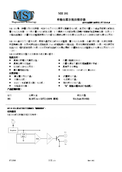
MH 181 是一种霍尔效应锁存器,可作为电子开关应用于无刷直流电动机。此芯片内置 1 个适合于磁感应的板载 霍尔电压发生器,1 个放大霍尔电压的比较器,1 个提供开关滞磁作用达到噪声抑制的施密特触发器,以及 1 个 开路输出端口。内置带隙调整器被用来为内部电压提供温度补偿馈源电压以及允许工作在较宽的电源电压范围。
-20V。
MH 181 的封装类型为无铅版本详述见第三部分。
性能总结:
z 具有对物理压力高抗击性;
z 内置开路前级驱动;
z 具有温度补偿性能;
z 内置电源输入管脚反相偏置保护功能;
z 较宽的工作电压范围;
z 具有尺寸小特性;
z 高质量和低价格;
z MH 181 KUA 100%的 125℃高温测试。
260
240
220
200
180 0
5 10 15 20 25 30
Time Wave Solder (Sec)
BH
BH-Supply Voltage
120
100 BH-80
BH-25
80
0
5
10 15 20 25 30
CDRH73NP-181MC中文资料

1.外形1-1.寸法図(mm)* 公差のない寸法は参考値とする。
1-2.捺印表示例 Q.推奨ランド寸法(mm)電極(端子)間の隙間はシルク処理をして御使用下さい。
2.コイル仕様2-1.端子接続図(裏面図)compliance Cd:Max.0.01wt%others:Max.0.1wt%RoHS12-2.電気的特性Ⅰ(リール梱包の場合)NO. 品 名 表 示 インダクタンス[以内]※1D.C.R.(Ω)[以下](at 20℃)※2定格電流(A)※3スミダコード0102 CDRH73NP-1ØØMCCDRH73NP-12ØMC10012010μH ± 20%12μH ± 20%72m (55m)98m (75m)1.681.524733-01544733-01550304 CDRH73NP-15ØMCCDRH73NP-18ØMC15018015μH ± 20%18μH ± 20%0.13 (96m)0.14 (0.11)1.331.204733-01564733-01570506 CDRH73NP-22ØMCCDRH73NP-27ØMC22027022μH ± 20%27μH ± 20%0.19 (0.15)0.21 (0.16)1.070.964733-01584733-01590708 CDRH73NP-33ØMCCDRH73NP-39ØMC33039033μH ± 20%39μH ± 20%0.24 (0.18)0.32 (0.25)0.910.774733-01604733-01610910 CDRH73NP-47ØMCCDRH73NP-56ØMC47056047μH ± 20%56μH ± 20%0.36 (0.28)0.47 (0.36)0.760.684733-01634733-01641112 CDRH73NP-68ØMCCDRH73NP-82ØMC68082068μH ± 20%82μH ± 20%0.52 (0.40)0.69 (0.53)0.610.574733-01654733-01661314 CDRH73NP-1Ø1MCCDRH73NP-121MC101121100μH ± 20%120μH ± 20%0.79 (0.61)0.89 (0.69)0.500.494733-01674733-01681516 CDRH73NP-151MCCDRH73NP-181MC151181150μH ± 20%180μH ± 20%1.27 (1.02)1.45 (1.16)0.430.394733-01694733-01701718 CDRH73NP-221MCCDRH73NP-271MC221271220μH ± 20%270μH ± 20%1.65 (1.32)2.31 (1.85)0.350.324733-01714733-01721920 CDRH73NP-331MCCDRH73NP-391MC331391330μH ± 20%390μH ± 20%2.62 (2.10)2.94 (2.35)0.280.264733-01744733-01752122 CDRH73NP-471MCCDRH73NP-561MC471561470μH ± 20%560μH ± 20%4.18 (3.35)4.67 (3.73)0.240.224733-01764733-01772324 CDRH73NP-681MCCDRH73NP-821MC681821680μH ± 20%820μH ± 20%5.73 (4.58)6.54 (5.23)0.190.184733-01784733-017925 CDRH73NP-1Ø2MC 102 1.0 mH ± 20% 9.44 (7.55)0.16 4733-01802-3.電気的特性Ⅱ(箱梱包の場合)NO. 品 名 表 示 インダクタンス[以内]※1D.C.R.(Ω)[以下](at 20℃)※2定格電流(A)※3スミダコード2627 CDRH73NP-1ØØMBCDRH73NP-12ØMB10012010μH ± 20%12μH ± 20%72m (55m)98m (75m)1.681.524733-01814733-01822829 CDRH73NP-15ØMBCDRH73NP-18ØMB15018015μH ± 20%18μH ± 20%0.13 (96m)0.14 (0.11)1.331.204733-01834733-01853031 CDRH73NP-22ØMBCDRH73NP-27ØMB22027022μH ± 20%27μH ± 20%0.19 (0.15)0.21 (0.16)1.070.964733-01864733-01873233 CDRH73NP-33ØMBCDRH73NP-39ØMB33039033μH ± 20%39μH ± 20%0.24 (0.18)0.32 (0.25)0.910.774733-01884733-01893435 CDRH73NP-47ØMBCDRH73NP-56ØMB47056047μH ± 20%56μH ± 20%0.36 (0.28)0.47 (0.36)0.760.684733-01904733-01913637 CDRH73NP-68ØMBCDRH73NP-82ØMB68082068μH ± 20%82μH ± 20%0.52 (0.40)0.69 (0.53)0.610.574733-01924733-01933839 CDRH73NP-1Ø1MBCDRH73NP-121MB101121100μH ± 20%120μH ± 20%0.79 (0.61)0.89 (0.69)0.500.494733-01944733-01964041 CDRH73NP-151MBCDRH73NP-181MB151181150μH ± 20%180μH ± 20%1.27 (1.02)1.45 (1.16)0.430.394733-01974733-01984243 CDRH73NP-221MBCDRH73NP-271MB221271220μH ± 20%270μH ± 20%1.65 (1.32)2.31 (1.85)0.350.324733-01994733-02004445 CDRH73NP-331MBCDRH73NP-391MB331391330μH ± 20%390μH ± 20%2.62 (2.10)2.94 (2.35)0.280.264733-02014733-02024647 CDRH73NP-471MBCDRH73NP-561MB471561470μH ± 20%560μH ± 20%4.18 (3.35)4.67 (3.73)0.240.224733-02034733-02044849 CDRH73NP-681MBCDRH73NP-821MB681821680μH ± 20%820μH ± 20%5.73 (4.58)6.54 (5.23)0.190.184733-02054733-020750 CDRH73NP-1Ø2MB 102 1.0 mH ± 20% 9.44 (7.55)0.16 4733-0208※1: 測定周波数 L at 1 kHz※2: ( )内は標準値とする。
- 1、下载文档前请自行甄别文档内容的完整性,平台不提供额外的编辑、内容补充、找答案等附加服务。
- 2、"仅部分预览"的文档,不可在线预览部分如存在完整性等问题,可反馈申请退款(可完整预览的文档不适用该条件!)。
- 3、如文档侵犯您的权益,请联系客服反馈,我们会尽快为您处理(人工客服工作时间:9:00-18:30)。
CDE Cornell Dubilier • 1605 E. Rodney French Blvd. • New Bedford, MA 02744 • Phone: (508)996-8561 • Fax: (508)996-3830 •
Type ESRH
Solid Polymer Aluminum SMT Capacitors
Solid P olymer A luminum capacitors are now available with a +125ºC temperature rating. CDE’s type ESRH capacitors are rated at +125ºC for 1000 hours when operated at 3/4 of the 105ºC rated voltage. Solid Polymer Aluminum electrolytic capacitors feature extremely low ESR which yields a capacitor with very low high frequency impedance and high ripple current capability. When low ESR is your requirement, one type ESRH capacitor can replace three or more tantalum or aluminum electrolytic capacitors. The solid electrolyte in a polymer aluminum capacitor results in a long (and ignition free) life, and the 7.3 x 4.3 footprint is compatible with “D” case solid tantalum capacitors.
Specifications
Markings
Operating Temperature Range:
Capacitance Tolerance:Dissipation Factor (DF):
Surge Voltage:
DC Leakage Current (after 2 minutes):
-55 ºC to +105 ºC at rated voltage (+125 ºC at .75 x rated voltage)±20% at 120 Hz and +20 ºC ≤0.10 at 120 Hz and +20 ºC 1.25 x rated voltage I ≤ .1 CV
ESRH
101
M
08
R
Packaging Code
CDE Type
Capacitance
Code Capacitance Tolerance WVDC Code
R = Tape & Reel 2000 pcs/reel
02 =2.0 Vdc 06 = 6.3 Vdc 680 = 68 µF M = ±20%
0E =2.5 Vdc 08 = 8.0 Vdc
101 = 100 µF
04 =4.0 Vdc
Lot Code
Capacitance
(“R” = Decimal Point)
元器件交易网
Type ESRH Solid Polymer Aluminum SMT Capacitors CDE Cornell Dubilier • 1605 E. Rodney French Blvd. • New Bedford, MA 02744 • Phone: (508)996-8561 • Fax: (508)996-3830 •
Low E.S.R. and High Temperature
Outline Drawing
Ratings
*12mm wide tape — 13” diameter reel
Capacitance
(µF)
Rated Voltage WVDC
Catalog Maximum Ripple Current Part Number E.S.R.at 100 kHz H ±0.2Tape* and Reel 100 kHz/20 ºC
+20 ºC to + 125 ºC
(mm)
(2000 pcs/reel)(Ω)
(A rms )
180 2.0ESRH181M02R 0.015 2.5 2.8150 2.5ESRH151M0ER 0.015 2.5 2.8120 4.0ESRH121M04R 0.015 2.5 2.8100 6.3ESRH101M06R 0.015 2.5 2.8688.0ESRH680M08R 0.015 2.5 2.8270 2.0ESRH271M02R 0.012 3.0 4.1220 2.5ESRH221M0ER 0.012 3.0 4.1180 4.0ESRH181M04R 0.012 3.0 4.1150 6.3ESRH151M06R 0.012 3.0 4.1100
8.0
ESRH101M08R
0.012
3.0
4.1
Markings
Land Pattern
元器件交易网
CDE Cornell Dubilier • 1605 E. Rodney French Blvd. • New Bedford, MA 02744 • Phone: (508)996-8561 • Fax: (508)996-3830 •
Type ESRH Solid Polymer Aluminum SMT Capacitors
Typical Impedance & ESR
Life Test:
Apply rated DC working voltage at 105 ºC (or 0.75 x WVDC at 125 ºC) for 1000 hours, and then stabilize them to +20 ºC. Capacitors will meet the following limits:
∆C = ±10% of the initial measured value DF & DCL ≤ the initial specified value
Shelf Life Test:
Shelf life is typically 5 to 10 years. Accelerated test:
after 500 hours at125 ºC, capacitors will meet the
following limits after stabilization at 20 ºC: ∆C = ±10% of the initial measured value DF & DCL ≤ the initial specified value
Moisture Resistance:
After 500 hours storage at +60 ºC and 90% R.H. without load, the capacitor will meet the following limits:
∆C = +70%/–20% of the initial measured value (2.0 & 2.5 Vdc),+60%/–20% of the initial measured value (4.0 Vdc), +50%/–20% of the initial measured value (6.3 Vdc), +40%/–20% of the initial measured value (8.0 Vdc).
DF ≤ two times the initial specified value DCL ≤ the initial specified value
Resistance to Soldering Heat:
Capacitors withstand being heated in an oven at 235 ºC for 200 seconds.
Soldering:
Solid Polymer Aluminum capacitors are designed for reflow soldering.
Preheat the capacitors at 160 ºC for a maximum of
120 seconds. The time at or above 200 ºC on the
surface of the capacitor should be per the
following chart:
Frequency (kHz)
ESRH271M02R 270 µF/2V
Impedance/ESR
ESRH680M02R 680 µF/2V
Impedance/ESR
Specifications (continued)
(For more information on this product see the Solid Polymer Aluminum Application Guide)
元器件交易网。