YHO-13351_1346753-00-1_DataSheet_MedChemExpress
3M7533丝印胶水质量控制手册

3M7533丝印胶水质量控制手册目标本质量控制手册旨在确保3M7533丝印胶水的生产和使用过程中的质量控制。
通过遵守本手册中的指导原则,能够保证产品质量的一致性和可靠性。
参考标准- ISO 9001:2015 质量管理体系标准- 3M7533丝印胶水技术规格质量控制原则1. 原材料选用:确保选用符合规格要求的原材料,并建立合格供应商名单,追踪原材料的来源和质量。
2. 生产过程控制:制定详细的生产手册,规定每个生产步骤的操作方法和质量要求,监控每个步骤的工艺参数。
3. 检验和测试:建立完善的检验和测试体系,对3M7533丝印胶水的关键性能进行定期检验和测试。
4. 设备维护:定期对生产设备进行维护和校准,确保设备的正常运行和准确性。
5. 不良品处理:制定不良品处理程序,对不合格产品进行处理和追踪,以及分析不良品原因并采取改进措施。
质量记录要求1. 原材料记录:对每批原材料进行记录,包括供应商信息、批号、质检报告等。
2. 生产记录:详细记录每个生产批次的日期、工艺参数、操作人员等信息。
3. 检验记录:对每批3M7533丝印胶水进行检验,并记录检验结果。
4. 不良品记录:对不合格产品进行记录,包括数量、原因、后续处理等。
培训和持续改进1. 培训计划:制定培训计划,确保员工了解质量控制要求和操作规程。
2. 内部审核:定期进行内部质量体系审核,发现问题并及时纠正。
3. 持续改进:通过持续改进措施,不断提高产品和过程的质量,提高客户满意度。
4. 客户反馈:定期收集客户反馈信息,分析问题并采取纠正措施。
质量控制的责任- 综合管理部门:负责制定质量目标和策略,确保质量控制的有效实施。
- 生产部门:负责生产过程中的质量控制和指导员工的操作。
- 质量部门:负责建立和维护质量管理体系,进行测试和不合格品管理。
- 培训部门:负责培训员工,确保员工了解质量控制要求和操作规程。
以上为本3M7533丝印胶水质量控制手册的主要内容,通过严格遵守手册中的指导原则,能够保证产品质量的稳定和一致性。
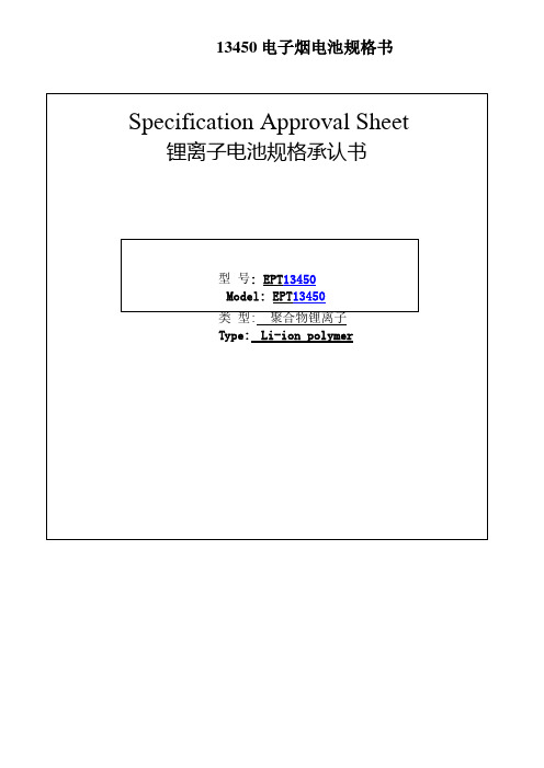
13450电子烟规格书
5.3.2Max. Charge Current最大充电电流
1.0CmA=650mA
Full charge condition: Constant current 0.2CmA to 4.2V, Constant voltage 4.2V to 0.05C in all at 25±2℃.
Temperature
存储温度
less than 1 month小于1个月
-10~+45℃
Recommended storage
temperature:20℃,at the
transportation
运输时存储温度为20℃。
less than 6 months小于6个月
-10~+35℃
4Outline Dimensions and Appearance电池外形尺寸及外观
4.2Appearance外观
There shall be no such defect as scratch, flaw, crack, rust, leakage, which may adversely affect
Commercial value of battery.
电池外表面清洁,无电解液泄漏,无明显的划痕及机械损伤,无变形,无影响电池价值的其它外观缺陷。
…………………………………………………
4
2.1
Product产品种类
………………………………………………………………
4
2.2
Model Name产品型号
………………………………………………………………
4
3
Ratings主要技术参数
………………………………………………………………
YHO-13351_DataSheet_MedChemExpress

Inhibitors, Agonists, Screening Libraries Data SheetBIOLOGICAL ACTIVITY:YHO–13351 is the water–soluble prodrug of YHO–13177, which is a potent and specific inhibitor of BCRP.IC50 value:Target: BCRP inhibitorin vitro: YHO–13177 potentiated the cytotoxicity of SN–38, mitoxantrone, and topotecan in both BCRP–transduced human colon cancer HCT116 (HCT116/BCRP) cells and SN–38–resistant human lung cancer A549 (A549/SN4) cells that express BCRP, but had little effect in the parental cells. In addition, YHO–13177 potentiated the cytotoxicity of SN–38 in human lung cancer NCI–H460 andNCI–H23, myeloma RPMI–8226, and pancreatic cancer AsPC–1 cells that intrinsically expressed BCRP. In contrast, it had no effect on P–glycoprotein–mediated paclitaxel resistance in MDR1–transduced human leukemia K562 cells and multidrug resistance–related protein 1–mediated doxorubicin resistance in MRP1–transfected human epidermoid cancer KB–3–1 cells. YHO–13177 increased the intracellular accumulation of Hoechst 33342, a substrate of BCRP, at 30 minutes and partially suppressed the expression of BCRP protein at more than 24 hours after its treatment in both HCT116/BCRP and A549/SN4 cells [1].in vivo: In mice, YHO–13351 was rapidly converted into YHO–13177 after its oral or intravenous administration. Coadministration of irinotecan with YHO–13351 significantly increased the survival time of mice inoculated with BCRP–transduced murine leukemia P388cells and suppressed the tumor growth in an HCT116/BCRP xenograft model, whereas irinotecan alone had little effect in these tumor models [1].PROTOCOL (Extracted from published papers and Only for reference)Animal study [1]:HCT116/BCRP cells (2 × 10⁶/mouse) were inoculated s.c. into the inguinal region of BALB/c nude mice. The long and short diameters of the tumor (mm) were measured using calipers, and tumor volume was estimated at various times with the following equation:......,When the tumor volume reached about 100 mm3 (day 0), the inoculated mice were divided into test groups (5 mice/group).Irinotecan was administered i.v. once a day on days 1, 5, and 9. YHO–13351 was administered orally at the same time as irinotecan or administered i.v. at 0 and 4 hours after irinotecan. On day 22 from the start of administration, a tumor was extirpated from each mouse and weighed, and the tumor growth inhibition rate, IR (%), was derived from the following equation:.References:[1]. Yamazaki R, et al. Novel acrylonitrile derivatives, YHO–13177 and YHO–13351, reverse BCRP/ABCG2–mediated drug resistance in vitro and in vivo. Mol Cancer Ther. 2011 Jul;10(7):1252–63.Product Name:YHO–13351Cat. No.:HY-12758CAS No.:1346753-00-1Molecular Formula:C 27H 37N 3O 7S 2Molecular Weight:579.73Target:BCRP Pathway:Membrane Transporter/Ion Channel Solubility:DMSO: ≥ 38 mg/mLCaution: Product has not been fully validated for medical applications. For research use only.Tel: 609-228-6898 Fax: 609-228-5909 E-mail: tech@Address: 1 Deer Park Dr, Suite Q, Monmouth Junction, NJ 08852, USA。
HL7133规格书xx

无负载
--
(除特殊注明以外:Ta=25℃)
最小 典型 最大 单位 测定
值
值
值
电路
1.455 1.5 1.545 V
1
10
mA
3
200
mV
0.05 0.2 %/V
负载稳定度
输出电压温度系 数
消耗电流 输入电压
VOUT IOUT Vdrop △VOUT1 △VIN·VOUT
△VOUT2
△VOUT △Ta·VOUT
ISS1 VIN
VIN= 5.3V,IOUT=10mA VIN= 5.3V
IOUT=1 mA 4.3V≤VIN≤15V
IOUT=1mA VIN=5.3V 1.0mA≤IOUT≤30mA VIN=5.3V,IOUT=10mA -40℃≤Ta≤85℃ VIN=15V
IOUT=1mA VIN=5.6V 1.0mA≤IOUT≤30mA VIN=5.6V,IOUT=10mA -40℃≤Ta≤85℃ VIN=15V
无负载
--
(除特殊注明以外:Ta=25℃)
最小 典型 最大 单位 测定
值
值
值
电路
3.492 3.6 3.708 V
1
30
mA
3
40
mV
1
0.05 0.2 %/V
■ 产品目录
型号
输出电压(注)
误差
H L7115
1.5V
H L7130
3.0V
H L7133
3.3V
H L7136
MJE15034G;MJE15035G;MJE15034;MJE15035;中文规格书,Datasheet资料
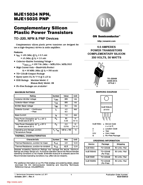
MJE15034 NPN,MJE15035 PNP Complementary Silicon Plastic Power Transistors TO−220, NPN & PNP DevicesComplementary silicon plastic power transistors are designed for use as high−frequency drivers in audio amplifiers.Features•h FE= 100 (Min) @ I C = 0.5 Adc= 10 (Min) @ I C = 2.0 Adc•Collector−Emitter Sustaining V oltage −V CEO(sus)= 350 Vdc (Min) − MJE15034, MJE15035•High Current Gain − Bandwidth Productf T = 30 MHz (Min) @ I C = 500 mAdc•TO−220AB Compact Package•Epoxy meets UL 94 V−0 @ 0.125 in•ESD Ratings:Machine Model: CHuman Body Model: 3B•Pb−Free Packages are Available*MAXIMUM RATINGSRating Symbol Value Unit Collector−Emitter Voltage V CEO350Vdc Collector−Base Voltage V CB350Vdc Emitter−Base Voltage V EB 5.0VdcCollector Current− Continuous− Peak I C 4.08.0AdcBase Current IB 1.0AdcTotal Power Dissipation @ T C = 25_C Derate above 25_C P D500.40WW/_CTotal Power Dissipation @ T A = 25_C Derate above 25_C P D 2.00.016WW/_COperating and Storage Junction Temperature Range TJ, T stg–65 to +150_CTHERMAL CHARACTERISTICSCharacteristic Symbol MaxUnitThermal Resistance, Junction−to−Case R q JC 2.5_C/W Thermal Resistance, Junction−to−Ambient R q JA62.5_C/W Stresses exceeding Maximum Ratings may damage the device. MaximumRatings are stress ratings only. Functional operation above the Recommended Operating Conditions is not implied. Extended exposure to stresses above the Recommended Operating Conditions may affect device reliability.*For additional information on our Pb−Free strategy and soldering details, please download the ON Semiconductor Soldering and Mounting Techniques Reference Manual, SOLDERRM/D.4.0 AMPERESPOWER TRANSISTORS COMPLEMENTARY SILICON 350 VOLTS, 50 WATTS Device Package ShippingORDERING INFORMATIONMJE15034TO−220AB50 Units / RailTO−220ABCASE 221ASTYLE 1MARKING DIAGRAMMJE1503x=Device Codex = 4 or 5A=Location CodeY=YearWW=Work WeekG=Pb−Free PackageMJE15035TO−220AB50 Units / Rail MJE15035G TO−220AB(Pb−Free)50 Units / Rail MJE15034G TO−220AB(Pb−Free)50 Units / RailELECTRICAL CHARACTERISTICS (T C = 25_C unless otherwise noted)CharacteristicSymbol Min Max Unit OFF CHARACTERISTICS Collector −Emitter Sustaining Voltage (Note 1)(I C = 10 mAdc, I B = 0)V CEO(sus)350−VdcCollector Cutoff Current (V CB = 350 Vdc, I E = 0)I CBO−10m Adc Emitter Cutoff Current (V BE = 5.0 Vdc, I C = 0)I EBO −10m AdcON CHARACTERISTICS (Note 1)DC Current Gain(I C = 0.1 Adc, V CE = 5.0 Vdc)(I C = 0.5 Adc, V CE = 5.0 Vdc)(I C = 1.0 Adc, V CE = 5.0 Vdc)(I C = 2.0 Adc, V CE = 5.0 Vdc)h FE1001005010−−−−−Collector −Emitter Saturation Voltage (I C = 1.0 Adc, I B = 0.1 Adc)V CE(sat)−0.5Vdc Base −Emitter On Voltage(I C = 1.0 Adc, V CE = 5.0 Vdc)V BE(on)−1.0VdcDYNAMIC CHARACTERISTICSCurrent Gain − Bandwidth Product (Note 2)(I C = 500 mAdc, V CE = 10 Vdc, f test = 1.0 MHz)f T30−MHz1.Pulse Test: Pulse Width v 300 m s, Duty Cycle v2.0%.2.f T = ⎪h fe ⎪• f test .Figure 1. Power Derating T, TEMPERATURE (°C)40T C 2060P D , P O W E R D I S S I P A T I O N (W A T T S )02.0T A 1.03.01.0101001000V CE , COLLECTOR −EMITTER VOLTAGE (V)I C , C O L L E C T O R C U R R E N T (A M P S )Figure 2. Active Region Safe Operating Areat, TIME (ms)r (t ), T R A N S I E N T T H E R M A L R E S I S T A N C E (N O R M A L I Z E D )Figure 3. Thermal Response0.010.1 1.010I C , COLLECTOR CURRENT (AMPS)V C E , C O L L E C T O R −E M I T T E R V O L T A G E (V )0.010.1 1.010I C , COLLECTOR CURRENT (AMPS)V C E , C O L L E C T O R −E M I T T E R V O L T A G E (V )0.010.1 1.010I C , COLLECTOR CURRENT (AMPS)h F E , D C C U R R E N T G A I N0.010.1 1.010I C , COLLECTOR CURRENT (AMPS)h F E , D C C U R R E N T G A I N0.010.1 1.010I C , COLLECTOR CURRENT (AMPS)h F E , D C C U R R E N T G A I N0.010.1 1.010I C , COLLECTOR CURRENT (AMPS)h F E , D C C U R R E N T G A I NFigure 4. DC Current Gain, V CE = 5.0 VNPN MJE15034Figure 5. DC Current Gain, V CE = 5.0 VPNP MJE15035Figure 6. DC Current Gain, V CE = 20 VNPN MJE15034Figure 7. DC Current Gain, V CE = 20 VPNP MJE15035Figure 8. V CE(sat)NPN MJE15034Figure 9. V CE(sat)PNP MJE150350.00.20.40.60.81.01.20.010.1 1.010I C , COLLECTOR CURRENT (AMPS)V B E (o n ), B A S E −E M I T T E R V O L T A G E (V )1.40.010.1 1.010I C , COLLECTOR CURRENT (AMPS)B A S E −E M I T T E R V O L T A G E (V )Figure 10. V BE(sat)NPN MJE15034Figure 11. V BE(sat)PNP MJE150350.010.1 1.010I C , COLLECTOR CURRENT (AMPS)B AS E −E M I TT E R V O L T A G E (V )Figure 12. V BE(on)NPN MJE15034Figure 13. V BE(on)PNP MJE150350.00.20.40.60.81.01.2I C , COLLECTOR CURRENT (AMPS)f T , C U R R E N T B A N D W I D T H P R O D U C T (M H z )0.1 1.0I C , COLLECTOR CURRENT (AMPS)f T , C U R R E N T B A N D W I D T H P R O D U C T (M H z )0.0010.0110Figure 14. Typical Current Gain Bandwidth ProductNPN MJE15034Figure 15. Typical Current Gain Bandwidth ProductPNP MJE150350.010.1 1.010I C , COLLECTOR CURRENT (AMPS)V B E (o n ), B A S E −E M I T T E R V O L T A G E (V )0.11.00.0010.0110PACKAGE DIMENSIONSTO −220CASE 221A −09ISSUE AGNOTES:1.DIMENSIONING AND TOLERANCING PER ANSI Y14.5M, 1982.2.CONTROLLING DIMENSION: INCH.3.DIMENSION Z DEFINES A ZONE WHERE ALL BODY AND LEAD IRREGULARITIES ARE ALLOWED.DIM MIN MAX MIN MAX MILLIMETERS INCHES A 0.5700.62014.4815.75B 0.3800.4059.6610.28C 0.1600.190 4.07 4.82D 0.0250.0360.640.91F 0.1420.161 3.61 4.09G 0.0950.105 2.42 2.66H 0.1100.161 2.80 4.10J 0.0140.0250.360.64K 0.5000.56212.7014.27L 0.0450.060 1.15 1.52N 0.1900.210 4.83 5.33Q 0.1000.120 2.54 3.04R 0.0800.110 2.04 2.79S 0.0450.055 1.15 1.39T 0.2350.255 5.97 6.47U 0.0000.0500.00 1.27V 0.045--- 1.15---Z---0.080--- 2.04FSEATING PLANESTYLE 1:PIN 1.BASE2.COLLECTOR3.EMITTER4.COLLECTORON Semiconductor and are registered trademarks of Semiconductor Components Industries, LLC (SCILLC). SCILLC reserves the right to make changes without further notice to any products herein. SCILLC makes no warranty, representation or guarantee regarding the suitability of its products for any particular purpose, nor does SCILLC assume any liability arising out of the application or use of any product or circuit, and specifically disclaims any and all liability, including without limitation special, consequential or incidental damages.“Typical” parameters which may be provided in SCILLC data sheets and/or specifications can and do vary in different applications and actual performance may vary over time. All operating parameters, including “Typicals” must be validated for each customer application by customer’s technical experts. SCILLC does not convey any license under its patent rights nor the rights of others. SCILLC products are not designed, intended, or authorized for use as components in systems intended for surgical implant into the body, or other applications intended to support or sustain life, or for any other application in which the failure of the SCILLC product could create a situation where personal injury or death may occur. Should Buyer purchase or use SCILLC products for any such unintended or unauthorized application, Buyer shall indemnify and hold SCILLC and its officers, employees, subsidiaries, affiliates,and distributors harmless against all claims, costs, damages, and expenses, and reasonable attorney fees arising out of, directly or indirectly, any claim of personal injury or death associated with such unintended or unauthorized use, even if such claim alleges that SCILLC was negligent regarding the design or manufacture of the part. SCILLC is an Equal Opportunity/Affirmative Action Employer. This literature is subject to all applicable copyright laws and is not for resale in any manner.PUBLICATION ORDERING INFORMATION分销商库存信息:ONSEMIMJE15034G MJE15035G MJE15034 MJE15035。
IT-170GRA datasheet-2014102101

0.87 (5.0)
0.70 (4.0)
0.80 (4.57) 0.70 (4.00) 0.55 (3.14)
106 -103
104 -103 ---
1.58 (9.0) 1.22 (7.0) 1.05 (6.0)
-1010 1010
-1010 1010 0.10 60
1.05 (6.00) 0.70 (4.00) 0.80 (4.57)
2.4.8 2.4.8.2 2.4.8.3
2.5.17.1
2.5.17.1 2.6.2.1 2.5.6
2.5.5.9 2.5.5.13
2.5.5.9 2.5.5.13
2.4.4
2.5.1 2.4.13.1 2.5.6.2
UL94 2.4.25 2.4.24.6 (5% wt loss) 2.4.24 2.4.24
--
ppm/˚C
60 maximum 300 maximum 3.0 maximum
ppm/˚C ppm/˚C
%
30 minimum 15 minimum
AABUS
Minutes Minutes Pass/Fail
900 900
ppm
1500
Test Method IPC-TM-650 (or as noted)
-104 103
-104 103 0.8 40
4.1
5.4
4.0
5.4
4.0
3.9
3.9
0.035
0.007 0.008 0.008 0.008 0.009
0.035
--
480-510
415
--
(69,600-73,950)
深圳希莱恒电解质说明书

型号:IMS-972 \IMS-972Popular \IMS-972Plus标准号:YZB/粤注册号:粤食药监械(准)字生产许可号:粤食药监械生产许号注册/生产地址:深圳市南山区蛇口工业大道兴华工业大厦7栋3B南侧电话:2 传真:5 邮编:518066售后服务单位:深圳市希莱恒医用电子有限公司目录前言 (2)一.概论 (3)序 (3)方法简介 (3)二.测量原理 (3)电极原理 (3)方法原理 (4)三.仪器简介 (4)四.试剂 (4)五.仪器的安装 (5)场地要求 (5)安装过程 (5)六.操作步骤 (6)开机 (6)系统冲洗 (7)活化 (7)系统标定和自诊断 (8)血样测定 (8)服务菜单 (10)七.仪器保养 (16)每日保养 (16)每周保养 (16)主要配件的保养 (16)八.注意事项 (16)操作过程中 (16)测定质控过程中 (17)环境方面 (17)保养过程中 (17)样品的收集和处理 (17)其它 (18)九.附录 (18)十.用户疑难解答 (19)附录一如何做好室间质控 (25)附录二程序框图 (27)附录三操作步骤及注意事项 (28)附图一电极的使用说明书 (29)附图二管道安装示意图 (30)附图三打印机安装说明 (31)前言尊敬的用户:感谢贵处选用本公司的产品——IMS-972系列电解质分析仪。
电解质系列分别为:IMS-972、IMS-972Popular、IMS-972Plus共三种型号。
用于离子钾、钠、氯、钙、锂、镁、pH、二氧化碳的检验,测试项目可任意组合。
产品标准号:YZB/粤产品注册号:粤食药监械(准)字生产许可号:粤食药监械生产许号为了更好使用仪器,敬请阅读以下内容:1)初次使用本仪器的用户,请务必先仔细阅读本手册;2)配合公司上门安装讲解的工程师,全面地掌握该仪器的操作与保养;3)此仪器必须由专人负责维护,并做好记录,配合我公司的售后服务工作;4)本说明书可用于IMS—972系列的A、B、C、D、E、F、G、H、I、J、K、L、M型仪器。
维沙依尧晟信西西7270DP新产品文件说明书
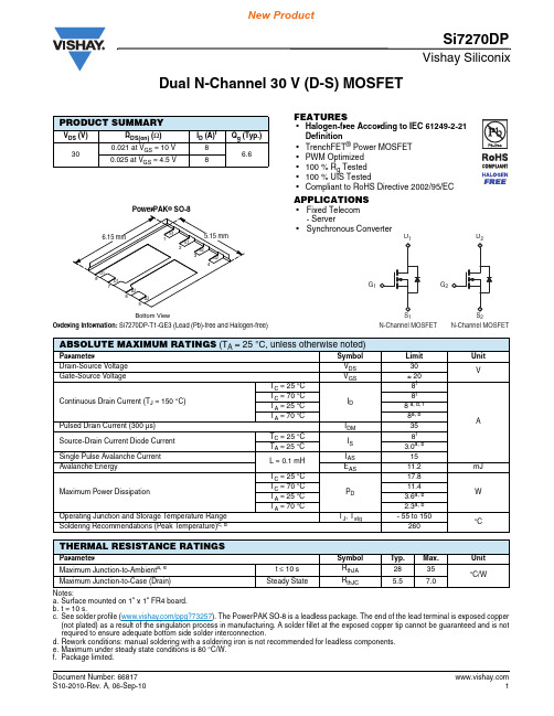
Vishay SiliconixSi7270DPDocument Number: Dual N-Channel 30 V (D-S) MOSFETFEATURES•Halogen-free According to IEC 61249-2-21Definition•TrenchFET ® Power MOSFET •PWM Optimized •100 % R g Tested •100 % UIS Tested•Compliant to RoHS Directive 2002/95/ECAPPLICATIONS•Fixed Telecom- Server•Notes:a.Surface mounted on 1" x 1" FR4 board.b.t = 10 s.c.See solder profile (/ppg?73257). The PowerPAK SO-8 is a leadless package. The end of the lead terminal is exposed copper (not plated) as a result of the singulation process in manufacturing. A solder fillet at the exposed copper tip cannot be guaranteed and is not required to ensure adequate bottom side solder interconnection.d.Rework conditions: manual soldering with a soldering iron is not recommended for leadless components.e.Maximum under steady state conditions is 80 °C/W.f.Package limited.PRODUCT SUMMARYV DS (V)R DS(on) (Ω)I D (A)f Q g (Typ.)300.021 at V GS = 10 V 8 6.60.025 at V GS = 4.5 V8ABSOLUTE MAXIMUM RATINGS (T A = 25 °C, unless otherwise noted)ParameterSymbol LimitUnit Drain-Source Voltage V DS30VGate-Source VoltageV GS ± 20Continuous Drain Current (T J = 150 °C)T C = 25 °C I D8f AT C = 70 °C 8fT A = 25 °C 8 a, b, f T A = 70 °C8a, bPulsed Drain Current (300 µs)I DM 35Source-Drain Current Diode Current T C = 25 °C I S8fT A = 25 °C 3.0a, bSingle Pulse Avalanche Current L = 0.1 mH I AS 15Avalanche EnergyE AS11.2mJ Maximum Power DissipationT C = 25 °C P D17.8WT C = 70 °C 11.4T A = 25 °C 3.6a, b T A = 70 °C 2.3a, bOperating Junction and Storage Temperature Range T J , T stg - 55 to 150°CSoldering Recommendations (Peak Temperature)c, d260THERMAL RESISTANCE RATINGSParameterSymbol Typ.Max.Unit Maximum Junction-to-Ambient a, e t ≤ 10 s R thJA 2835°C/WMaximum Junction-to-Case (Drain)Steady StateR thJC5.57.0 Document Number: 66817Vishay SiliconixSi7270DPNotes:a. Guaranteed by design, not subject to production testing.b. Pulse test; pulse width ≤ 300 µs, duty cycle ≤ 2 %.Stresses beyond those listed under “Absolute Maximum Ratings” may cause permanent damage to the device. These are stress ratings only, and functional operation of the device at these or any other conditions beyond those indicated in the operational sections of the specifications is not implied. Exposure to absolute maximum rating conditions for extended periods may affect device reliability.SPECIFICATIONS (T J = 25 °C, unless otherwise noted)Parameter Symbol Test Conditions Min. Typ.Max.Unit StaticDrain-Source Breakdown Voltage V DS V GS = 0 V , I D = 250 µA 30V V DS Temperature Coefficient ΔV DS /T J I D = 250 µA 34mV/°C V GS(th) Temperature Coefficient ΔV GS(th)/T J I D = 250 µA - 5.5Gate Threshold Voltage V GS(th) V DS = V GS , I D = 250 µA 1.22.8V Gate-Body LeakageI GSS V DS = 0 V , V GS = ± 20 V 100nA Zero Gate Voltage Drain Current I DSS V DS = 30 V, V GS = 0 V 1µA V DS = 30 V , V GS = 0 V , T J = 85 °C10On-State Drain Current bI D(on) V DS ≥ 5 V , V GS = 10 V 20A Drain-Source On-State Resistance b R DS(on) V GS = 10 V , I D = 8 A 0.01750.021ΩV GS = 4.5 V, I D = 6 A 0.02050.025Forward T ransconductance b g fs V DS = 10 V , I D = 8 A31SDynamicaInput Capacitance C iss V DS = 15 V, V GS = 0 V , f = 1 MHz 900pFOutput CapacitanceC oss 150Reverse Transfer Capacitance C rss 60Total Gate Charge Q g V DS = 15 V , V GS = 10 V , ID = 10 A 1421nCV DS = 15 V , V GS = 4.5 V, I D = 10 A6.610Gate-Source Charge Q gs 2.5Gate-Drain Charge Q gd 1.7Gate Resistance R g f = 1 MHz0.31.42.8ΩTurn-On Delay Time t d(on) V DD = 15 V , R L = 1.5 Ω I D ≅ 10 A, V GEN = 4.5 V , R g = 1 Ω1428nsRise Timet r 1020Turn-Off Delay Time t d(off) 1530Fall Timet f 816Turn-On Delay Time t d(on) V DD = 15 V , R L = 1.5 Ω I D ≅ 10 A, V GEN = 10 V , R g = 1 Ω1020Rise Timet r 816Turn-Off Delay Time t d(off) 1836Fall Timet f 816Drain-Source Body Diode Characteristics Continuous Source-Drain Diode Current I S T C = 25 °C 8A Pulse Diode Forward Current aI SM 35Body Diode VoltageV SD I S = 3 A0.77 1.2V Body Diode Reverse Recovery Time t rr I F = 5 A, dI/dt = 100 A/µs, T J = 25 °C1326ns Body Diode Reverse Recovery Charge Q rr 6.513nC Reverse Recovery Fall Time t a 8nsReverse Recovery Rise Timet b5Document Number: Vishay SiliconixSi7270DPTYPICAL CHARACTERISTICS (25°C, unless otherwise noted)Output CharacteristicsOn-Resistance vs. Drain CurrentGate ChargeTransfer CharacteristicsOn-Resistance vs. Junction Temperature Document Number: 66817Vishay SiliconixSi7270DPTYPICAL CHARACTERISTICS (25°C, unless otherwise noted)Source-Drain Diode Forward VoltageThreshold VoltageOn-Resistance vs. Gate-to-Source VoltageDocument Number: Vishay SiliconixSi7270DPTYPICAL CHARACTERISTICS (25°C, unless otherwise noted)* The power dissipation P D is based on T J(max.) = 150 °C, using junction-to-case thermal resistance, and is more useful in settling the upper dissipation limit for cases where additional heatsinking is used. It is used to determine the current rating, when this rating falls below the package limit.Current Derating*Power Derating, Junction-to-CasePower Derating, Junction-to-AmbientSi7270DPVishay SiliconixTYPICAL CHARACTERISTICS (25°C, unless otherwise noted)Normalized Thermal Transient Impedance, Junction-to-CaseVishay Siliconix maintains worldwide manufacturing capability. Products may be manufactured at one of several qualified locations. Reliability data for Silicon Technology and Package Reliability represent a composite of all qualified locations. For related documents such as package/tape drawings, part marking, and reliability data, see /ppg?66817. Document Number: 66817Package Information Vishay SiliconixPowerPAK® SO-8, (Single/Dual)Revison: 20-May-131Document Number: 71655Application Note 826Vishay SiliconixA P P L I C A T I O N N O T ERECOMMENDED MINIMUM PADS FOR PowerPAK ® SO-8 DualLegal Disclaimer Notice VishayDisclaimerALL PRODU CT, PRODU CT SPECIFICATIONS AND DATA ARE SU BJECT TO CHANGE WITHOU T NOTICE TO IMPROVE RELIABILITY, FUNCTION OR DESIGN OR OTHERWISE.Vishay Intertechnology, Inc., its affiliates, agents, and employees, and all persons acting on its or their behalf (collectively,“Vishay”), disclaim any and all liability for any errors, inaccuracies or incompleteness contained in any datasheet or in any other disclosure relating to any product.Vishay makes no warranty, representation or guarantee regarding the suitability of the products for any particular purpose or the continuing production of any product. To the maximum extent permitted by applicable law, Vishay disclaims (i) any and all liability arising out of the application or use of any product, (ii) any and all liability, including without limitation special, consequential or incidental damages, and (iii) any and all implied warranties, including warranties of fitness for particular purpose, non-infringement and merchantability.Statements regarding the suitability of products for certain types of applications are based on Vishay’s knowledge of typical requirements that are often placed on Vishay products in generic applications. Such statements are not binding statements about the suitability of products for a particular application. It is the customer’s responsibility to validate that a particular product with the properties described in the product specification is suitable for use in a particular application. Parameters provided in datasheets and/or specifications may vary in different applications and performance may vary over time. All operating parameters, including typical parameters, must be validated for each customer application by the customer’s technical experts. Product specifications do not expand or otherwise modify Vishay’s terms and conditions of purchase, including but not limited to the warranty expressed therein.Except as expressly indicated in writing, Vishay products are not designed for use in medical, life-saving, or life-sustaining applications or for any other application in which the failure of the Vishay product could result in personal injury or death. Customers using or selling Vishay products not expressly indicated for use in such applications do so at their own risk. Please contact authorized Vishay personnel to obtain written terms and conditions regarding products designed for such applications. No license, express or implied, by estoppel or otherwise, to any intellectual property rights is granted by this document or by any conduct of Vishay. Product names and markings noted herein may be trademarks of their respective owners.Material Category PolicyVishay Intertechnology, Inc. hereby certifies that all its products that are identified as RoHS-Compliant fulfill the definitions and restrictions defined under Directive 2011/65/EU of The European Parliament and of the Council of June 8, 2011 on the restriction of the use of certain hazardous substances in electrical and electronic equipment (EEE) - recast, unless otherwise specified as non-compliant.Please note that some Vishay documentation may still make reference to RoHS Directive 2002/95/EC. We confirm that all the products identified as being compliant to Directive 2002/95/EC conform to Directive 2011/65/EU.Vishay Intertechnology, Inc. hereby certifies that all its products that are identified as Halogen-Free follow Halogen-Free requirements as per JEDEC JS709A standards. Please note that some Vishay documentation may still make reference to the IEC 61249-2-21 definition. We confirm that all the products identified as being compliant to IEC 61249-2-21 conform to JEDEC JS709A standards.Revision: 02-Oct-121Document Number: 91000。
- 1、下载文档前请自行甄别文档内容的完整性,平台不提供额外的编辑、内容补充、找答案等附加服务。
- 2、"仅部分预览"的文档,不可在线预览部分如存在完整性等问题,可反馈申请退款(可完整预览的文档不适用该条件!)。
- 3、如文档侵犯您的权益,请联系客服反馈,我们会尽快为您处理(人工客服工作时间:9:00-18:30)。
Байду номын сангаас
Mechanisms: Pathways:Others; Target:BCRP Biological Activity: YHO-13351 is the water-soluble prodrug of YHO-13177, which is a potent and specific inhibitor of BCRP. IC50 value: Target: BCRP inhibitor in vitro: YHO-13177 potentiated the cytotoxicity of SN-38, mitoxantrone, and topotecan in both BCRPtransduced human colon cancer HCT116 (HCT116/BCRP) cells and SN-38–resistant human lung cancer A549 (A549/SN4) cells that express BCRP, but had little effect in the parental cells. In addition, YHO-13177 potentiated the cytotoxicity of SN-38 in human lung cancer NCI-H460 and NCI-H23, myeloma RPMI-8226, and pancreatic cancer AsPC-1 cells that intrinsically expressed BCRP. In contrast, it had no effect on Pglycoprotein–mediated paclitaxel resistance in MDR1-transduced human leukemia K562 cells and multidrug resistance-related protein 1–mediated doxorubicin resistance in MRP1-transfected human epidermoid cancer KB-3-1 cells. YHO-13177 i... References: [1]. Yamazaki R, et al. Novel acrylonitrile derivatives, YHO-13177 and YHO-13351, reverse BCRP/ABCG2mediated drug resistance in vitro and in vivo. Mol Cancer Ther. 2011 Jul;10(7):1252-63.
Caution: Not fully tested. For research purposes only Medchemexpress LLC
m o c . s s e r p x e m e h c d e Am S. Uw ,w 2 5w 8: 8b 0e JW Nm ,o n c o. i s t s c e nr up Jx he t m u e oh mc nd oe Mm D@ 2 0o f n 1i el : t i i a u Sm ,E e v i r D k r a P r e e D 1 1
Product Data Sheet
Product Name: CAS No.: Cat. No.: MWt: Formula: Purity :
YHO-13351 1346753-00-1 HY-12758 579.73 C27H37N3O7S2 >98%
Solubility:
Soluble in water