上海三花演示中文版20071123
MST Use Case Ex v1

39899 Balentine Drive, Suite 125 Phone: 510 651 5122 Newark, CA 94560 Fax: 510 651 5127URL: MST Use Case ExampleVersion 118 January 2011PurposeThis is a companion document to DisplayPort Standard Version 1.2 and provides tangible examples of how a topology consisting of MST DP devices is to be managed while DisplayPort Standard describes the overall framework.SummaryThis document is Version 1 of the MST DP Usage Example Document Series, and covers how an MST DP Source device and a device containing MST Branching Unit are to interact with each other to perform typical topology and payload bandwidth management functions. A topology consisting of an MST DP Source device, an MST Splitter Branch device, and two video stream sinks is covered in this document.Table of ContentsPreface (7)Acknowledgements (8)Revision History (9)References (10)1 Example MST Topology without Audio Stream Sink (11)1.1 Topology Change Sequences of This Document (14)1.2 Topology Discovery (14)1.2.1 Source Device Operation (14)1.2.2 Splitter Branch Device Operation (21)1.3 Reading and Writing DP Device Global Unique Identifier (GUID) (21)1.3.1 Source Device Operation (22)1.3.2 Splitter Branch Device Operation (24)1.4 Obtaining Display Capabilities (25)1.4.1 Source Device Operation (25)1.4.2 Splitter Branch Device Operation (30)1.5 Establishing a Virtual Channel from PC to Display 1 (31)1.5.1 Source Device Operation (31)1.5.2 Splitter Branch Device Operation (36)1.6 Establishing a Virtual Channel from PC to Display 2 (37)1.6.1 Source Device Operation (37)1.6.2 Splitter Branch Device Operation (41)1.7 Reallocating the Virtual Channel from PC to Display 1 (41)1.7.1 Source Device (41)1.7.2 Splitter Branch Device Operation (45)1.8 Deleting Virtual Channel from PC to Display 1 (45)1.8.1 Source Device (45)1.8.2 Splitter Branch Device Operation (47)1.9 Cloning the Virtual Channel from PC to Display 2 on Display 1 (47)1.9.1 Source Device Operation (47)1.9.2 Splitter Branch Device Operation (49)1.10 Deleting Cloned Virtual Channel from PC to Display 2 (49)1.10.1 Source Device Operation (49)1.10.2 Splitter Branch Device Operation (50)1.11 Handling Unexpected Changes in Available PBN (51)1.11.1 Splitter Branch Device Operation (51)1.11.2 Source Device Operation (52)1.12 Entering and Exiting Sleep Mode (53)1.12.1 Source Device Operation (53)1.12.2 Splitter Branch Device Operation (56)1.13 Connection Status Change of a Remote Device Due to Unplug or Power Off Event (57)1.13.1 Splitter Branch Device Operation (57)1.13.2 Source Device Operation (58)1.14 Connection Status Change of a Remote Device Due to Plug or Power On Event (59)1.14.1 Splitter Branch Device Operation (59)1.14.2 Source Device Operation (60)2 Example MST Topology with Audio (62)2.1 Topology Discovery (63)2.2 Establishing a Virtual Channel from PC to Display 1 with Audio (66)2.3 Establishing a Virtual Channel from PC to Display 2 with Audio (67)3 Native AUX Transactions for Sideband MSG Delivery (69)3.1 Sideband MSG From uPacket TX to uPacket RX (DOWN_REQ or UP_REP) (69)3.2 Sideband MSG From uPacket RX to uPacket TX (UP_REQ or DOWN_REP) (69)4 Appendix A: MST Source Device Acting as SST-mode-only Device (70)5 Appendix B: MST Source Device with Two DP Output Connectors (71)TablesTable 0-1: Main Contributors (8)Table 1-1: Reference Documents (10)Table 1-1: LINK_ADDRESS Message Transaction (17)Table 1-2: LINK_ADDRESS Message Transaction Sideband MSG (17)Table 1-3: LINK_ADDRESS Message Transaction Reply (17)Table 1-4: LINK_ADDRESS Message Transaction Reply First Sideband MSG (19)Table 1-5: LINK_ADDRESS Message Transaction Reply Second Sideband MSG (20)Table 1-6: Sideband MSG for the GUID REMOTE_DPCD_READ Message Transaction Request 22 Table 1-7: Sideband MSG for the GUID REMOTE_DPCD_READ Message Transaction Reply (22)Table 1-8: Sideband MSG for the GUID REMOTE_DPCD_WRITE Message Transaction Request23 Table 1-9: Sideband MSG for the GUID REMOTE_DPCD_Write Message Transaction Reply (24)Table 1-10: Sideband MSG for the REMOTE_DPCD_WRITE Message Transaction Request Setting the I2C Speed to 100K (25)Table 1-11: Sideband MSG for the REMOTE_DPCD_WRITE Message Transaction Reply (26)Table 1-12: Message Transaction Request for Reading 128-Byte EDID from a Remote Sink Device26 Table 1-13: Sideband MSG for REMOTE_I2C_READ Message Transaction Request (27)Table 1-14: First Sideband MSG Reply for REMOTE_I2C_READ Message Transaction (28)Table 1-15: Second Sideband MSG Reply for REMOTE_I2C_READ Message Transaction (28)Table 1-16: Third Sideband MSG Reply for REMOTE_I2C_READ Message Transaction (29)Table 1-17: Fourth Sideband MSG Reply for REMOTE_I2C_READ Message Transaction Reply . 29 Table 1-18: ENUM_PATH_RESOURCES Message Transaction Request Sideband MSG (31)Table 1-19: ENUM_PATH_RESOURCES Message Transaction Reply Sideband MSG (32)Table 1-20: Virtual Channel (VC) Payload ID Table (35)Table 1-21: ALLOCATE_PAYLOAD Message Transaction Request Sideband MSG (35)Table 1-22: ALLOCATE_PAYLOAD Message Transaction Reply Sideband MSG (36)Table 1-23: ENUM_PATH_RESOURCES Message Transaction Request Sideband MSG (37)Table 1-24: ENUM_PATH_RESOURCES Message Transaction Reply Sideband MSG (38)Table 1-25: uPacket TX and RX VC Payload ID Table (39)Table 1-26: ALLOCATE_PAYLOAD Message Transaction Request Sideband MSG (40)Table 1-27: ALLOCATE_PAYLOAD Message Transaction Reply Sideband MSG (40)Table 1-28: uPacket TX and RX VC Payload ID Table (42)Table 1-29: ALLOCATE_PAYLOAD Message Transaction Request Sideband MSG for Reallocating a Virtual Channel (44)Table 1-30: ALLOCATE_PAYLOAD Message Transaction Reply Sideband MSG for Reallocatinga Virtual Channel (44)Table 1-31: Delete VC ALLOCATE_PAYLOAD Message Transaction Request Sideband MSG .. 45 Table 1-32: Delete VC ALLOCATE_PAYLOAD Message Transaction Reply Sideband MSG (46)Table 1-33: uPacket TX and uPacket RX VC Payload ID Table (47)Table 1-34: ALLOCATE_PAYLOAD Message Transaction Request Sideband MSG for Cloning Example (48)Table 1-35: ALLOCATE_PAYLOAD Message Transaction Reply Sideband MSG for Cloning Example (48)Table 1-36: ALLOCATE_PAYLOAD Message Transaction Request Sideband MSG for Deleting a Cloned Virtual Channel Example (49)Table 1-37: ALLOCATE_PAYLOAD Message Transaction Reply Sideband MSG for Deleting a Cloned Virtual Channel Example (50)Table 1-38: RESOURCE_STATUS_NOTIFY Message Transaction Request Sideband MSG (51)Table 1-39: RESOURCE_STATUS_NOTIFY Message Transaction Reply Sideband MSG (52)Table 1-40: POWER_DOWN_PHY Message Transaction Request Sideband MSG (53)Table 1-41: POWER_DOWN_PHY Message Transaction Reply Sideband MSG (53)Table 1-42: CLEAR_PAYLOAD_ID_TABLE Message Transaction Request Sideband MSG (54)Table 1-43: CLEAR_PAYLOAD_ID_TABLE Message Transaction Reply Sideband MSG (55)Table 1-44: POWER_UP_PHY Message Transaction Request Sideband MSG (55)Table 1-45: POWER_UP_PHY Message Transaction Reply Sideband MSG (56)Table 1-46: Unplug CONNECTION_STATUS_NOTIFY Broadcast Message Transaction Request Sideband MSG (57)Table 1-47: Unplug CONNECTION_STATUS_NOTIFY Broadcast Message Transaction Reply Sideband MSG (58)Table 1-48: Plug CONNECTION_STATUS_NOTIFY Broadcast Message Transaction Request Sideband MSG (59)Table 1-49: Plug CONNECTION_STATUS_NOTIFY Broadcast Message Transaction Reply Sideband MSG (60)Table 2-1: Audio Video Support Requirements (63)Table 2-2: LINK_ADDRESS Message Transaction Reply First Sideband MSG (64)Table 2-3: LINK_ADDRESS Message Transaction Reply Second Sideband MSG (65)Table 2-4: ALLOCATE_PAYLOAD Message Transaction Request Sideband MSG with Audio (66)Table 2-5: ALLOCATE_PAYLOAD Message Transaction Reply Sideband MSG (66)Table 2-6: ALLOCATE_PAYLOAD Message Transaction Request Sideband MSG with Audio (67)Table 2-7: ALLOCATE_PAYLOAD Message Transaction Reply Sideband MSG (68)FiguresFigure 1-1: Logical Topology Covered in this Document (11)Figure 1-2: Physical Topology of PC and Multi-stream Sink Monitor (12)Figure 1-3: Physical Topology of PC and Multi-stream Sink Monitor (13)Figure 1-4: Physical Topology with Separate PC, Branch Device and Single Stream DP Monitors .. 13 Figure 1-5: Determine Whether LINK_ADDRESS Message Transaction Should be Used (15)Figure 1-6: Virtual Channel Allocation Procedure Flowchart (34)Figure 2-1: Audio Example Topology (62)PrefaceIntellectual PropertyCopyright © 2011 Video Electronics Standards Association. All rights reserved.While every precaution has been taken in the preparation of this standard, the Video Electronics Standards Association and its contributors assume no responsibility for errors or omissions, and make no warranties, expressed or implied, of functionality or suitability for any purpose.TrademarksAll trademarks used within this document are the property of their respective owners. DMT, DP, DisplayPort, EDID, and VESA are trademarks of the Video Electronics Standards Association.HDCP is a trademark of Digital Content Protection, LLCI2C is a trademark of Philips.PatentsVESA draws attention to the fact that it is claimed that compliance with this Standard may involve the use of a patent or other intellectual property right (collectively, “IPR”). VESA takes no position concerning the evidence, validity, and scope of this IPR.THIS STANDARD IS BEING OFFERED WITHOUT ANY WARRANTY WHATSOEVER, AND IN PARTICULAR, ANY WARRANTY OF NON-INFRINGEMENT IS EXPRESSLY DISCLAIMED. ANY IMPLEMENTATION OF THIS STANDARD SHALL BE MADE ENTIRELY AT THE IMPLEMENTER’S OWN RISK, AND NEITHER VESA, NOR ANY OF ITS MEMBERS OR SUBMITTERS, SHALL HAVE ANY LIABILITY WHATSOEVER TO ANY IMPLEMENTER OR THIRD PARTY FOR ANY DAMAGES OF ANY NATURE WHATSOEVER DIRECTLY OR INDIRECTLY ARISING FROM THE IMPLEMENTATION OF THIS STANDARD.Support for this StandardClarifications and application notes to support this standard may be written. To obtain the latest standard and any support documentation, contact VESA.If you have a product, which incorporates DisplayPort, you should ask the company that manufactured your product for assistance. If you are a manufacturer, VESA can assist you with any clarification you may require. Submit all comments or reported errors in writing to VESA using one of the following methods.•Fax: 510 651 5127, direct this fax to Technical Support at VESA•e-mail: support@•Mail: Technical SupportVESA39899 Balentine Drive, Suite 125Newark, CA 94560AcknowledgementsThis document would not have been possible without the efforts of VESA’s DisplayPort Task Group. In particular, the following individuals and their companies contributed significant time and knowledge to this version of the document.Table 0-1: Main ContributorsName CompanyTony Cheng AMDSyed Hussain AMDGeorge Kyriazis AppleBob Ridenour AppleYoshinobu Banba EIZO NANAOGeorge Hayek IntelSrikanth Kambhatla IntelCameron Buschardth NVIDIADavid Steers NVIDIAKen Jaramillo NXP SemiconductorJohn Garrett STMicroelectronics EditorAlan Kobayashi STMicroelectronics Co-editorRevision HistoryJanuary 18, 2011Initial ReleaseReferencesTable 1-2: Reference DocumentsDocument Version / Revision Date VESA Policy 200 Intellectual Property Rights Version B February 2005 VESA DisplayPort Standard Version 1.2 January 2010VESA and Industry Standards and Guidelines for Computer Display MonitorVersion 1. Rev.12 November 2008 Timing (DMTVESA Enhanced Extended Display Identification Data Standard (E-EDID) Rel. A Version 1 February 20001 Example MST Topology without Audio Stream SinkThis document covers how an MST DP Source device and a device containing MST Branching Unit are to interact to perform typical topology and payload bandwidth management functions in the following logical topology.Figure 1-4: Physical Topology with Separate PC, Branch Device and Single Stream DPMonitors1.1 Topology Change Sequences of This DocumentThere are two ways an MST DP Source device can be notified of a topology change.By a Hot Plug/Unplug event indicating a connection or disconnection of an immediate downstream device to its uPacket TX port.By receipt of a CONNECTION_STATUS_NOTIFY message transaction indicating a connection or disconnection of a remote device.Note: Alternately, the Topology Manager in a Source device may choose to periodically poll theUP_REQ_RDY bit of the immediate downstream device to monitor the connection change event.In this document, topology discovery and ensuing operations upon a plugging of an immediatedownstream device (that is, the Splitter to which to stream sinks are already connected) to an MST DP Source device is covered first. Connection status change of a remote device is covered later in thisdocument.1.2 Topology DiscoveryThis example explains the sequence of events necessary to discover the connected stream sinks. It is assumed that both stream sinks are connected to the branching unit before the branching unit isconnected to the source device.1.2.1Source Device OperationWhen the Splitter is plugged to the MST DP Source device, the Source device is notified of a HotPlug event via the detection of a long (that is, longer than 2ms) HPD pulse. Topology Manager of the DP Source device will read certain DPCD locations of the Splitter to determine the newly connected device type so that it can update the topology map to its Stream Policy Maker.The DPCD locations to be read for topology discovery are DPCD_REV,DOWNSTREAMPORT_PRESENT and MSTM_CAP. The given DPCD locations are read todetermine what type of DP device was connected and whether the device is MST capable (and thus capable of handling message transactions using Sideband MSGs) as shown in the following diagram.With the logical topology used in this document, the immediate downstream device has an MSTBranching Unit. Once it is determined that the device has an MST Branching Unit, the TopologyManager of the MST Source device must use the LINK_ADDRESS Message transaction to discover the devices connected to the Branching Unit.Figure 1-5: Determine Whether LINK_ADDRESS Message Transaction Should be Used The MST DP Source device sets UP_REQ_EN bit and UPSTREAM_IS_SRC bit of the immediate downstream device to declare itself as an MST DP Source device before issuing theLINK_ADDRESS Message Transaction to the immediate downstream device. The MST DP Sourcedevice uses the information received from the LINK_ADDRESS Message transaction to determine whether other DP MST Branching units are connected. If other DPMST Branching units are discovered, the LINK_ADDRESS Message transaction is sent to each DP MST Branching unit to determine the device connected to it. This procedure continues until the Source device’s search goals are met (all sinks found, first sink found or some other goal).An example algorithm to find all connected sinks is given below.Procedure FindAccessibleDPDevices given RAD of MST DP Branch device Send LINK_ADDRESS Message to address of MST DP Branching UnitWait wait_time_out time period (4 sec.) or until LINK_ADDRESS Message reply if wait_time_out time period elapsed without LINK_ADDRESS Message reply exit procedure indicating failureendifif device GUID field is empty (zeros)Write a GUID into the deviceelseif device already in list of devices foundif duplicate GUID obtained by traversing a loopexit procedure indicating a loopelseThere are multiple paths to the same deviceexit procedureendifendifendifAdd device to list of devices foundfor each downstream port of the MST DP Branch deviceif MST Branching Unit connected to downstream portExecute FindAccessibleDPDevices with address of MST DP Branch device elseAdd device to list of stream sinks/SST DP devicesendifendforend procedureThe Message Transaction source device will wait for 4 seconds for a reply for all message transactions. This is the time period to wait for the entire message transaction reply to be received; in other words, the wait time period for the last Sideband MSG for the message transaction reply to be received by the message source device.Given two RADs for the same DP MST device (same GUID), the following procedure will determine whether the DP MST device is part of a loop or is accessible through multiple paths.Procedure IsDevicePartOfLoop given RAD1 and RAD2 to same DP MST device if RAD1 has fewer links than RAD2Set SmallerRAD to RAD1Set LargerRAD to RAD2elseSet SmallerRAD to RAD2Set LargerRAD to RAD1endifSet N to the number of links in SmallerRADif the first N links of SmallerRAD is the same as the N links of LargerRAD return trueendifreturn falseend procedureThe list of sinks and SST DP devices from the above procedure will contain the relative address for the two stream sinks in this examples topology. The LINK_ADDRESS Message Transaction request and reply for this example are shown below.Table 1-1: LINK_ADDRESS Message TransactionLINK_ADDRESS Message Transaction Request Field Name ValueZeroRequest_Identifier 0000 0001Table 1-2: LINK_ADDRESS Message Transaction Sideband MSG LINK_ADDRESS Message Transaction Sideband MSG Request Field Name ValueLink_Count_TotalLink_Count_RemainingNo RADBroadcast_MessagePath_MessageSideband_MSG_Body_Length Start_Of_Message_Transaction End_Of_Message_Transaction zeroMessage_Sequence_No Sideband_MSG_Header_CRC zeroRequest_IdentifierSideband_MSG_Data_CRC 0001 000000 0010 111011000 0001 1101 0101The following shows the above values grouped into bytes.10h 02h CBh 01h D5hThe following LINK_ADDRESS Message Transaction reply will be received for the physical topology consisting of a PC connected to a daisy chainable monitor with an attached SST DP Monitor.Table 1-3: LINK_ADDRESS Message Transaction ReplyLINK_ADDRESS Message Transaction Reply Field Name ValueReply_TypeRequest_IdentifierGlobal_Unique_Identifier (GUID) of the originating branch device zerosNumber_Of_PortsInput_Port[0]Peer_Device_Type[0]Port_Number[0]Messaging_Capability_Status[0] 0000 0001 0000 0001 0000 0010 0000 0011 0000 0100 0000 0101 0000 0110 0000 0111 0000 1000 0000 1001 0000 1010 0000 1011 0000 1100 0000 1101 0000 1110 0000 1111 0001 0000 0000 00111001 00001DisplayPort_Device_Plug_Status[0]zerosInput_Port[1]Peer_Device_Type[1]Port_Number[1]Messaging_Capability_Status[1]DisplayPort_Device_Plug_Status[1]Legacy_Device_Plug_Status[1]zerosDPCD_Revision[1]Peer_Global_Unique_Identifier[1]Number_SDP_Streams[1]Number_SDP_Stream_Sinks[1]Input_Port[2]Peer_Device_Type[2]Port_Number[2]Messaging_Capability_Status[2]DisplayPort_Device_Plug_Status[2]Legacy_Device_Plug_Status[2]zerosDPCD_Revision[2]Peer_Global_Unique_Identifier[2] (Same as branch unit since this is a logical port) Number_SDP_Streams[2]Number_SDP_Stream_Sinks[2] 100 0000 0011 000110 0000 0001 0010 0000 0000 0000 0000 0000 0000 0000 0000 0000 0000 0000 0000 0000 0000 0000 0000 0000 0000 0000 0000 0000 0000 0000 0000 0000 0000 0000 0000 0000 0000 0000 0000 0000 0000011 100010 0000 0001 0010 0000 0001 0000 0010 0000 0011 0000 0100 0000 0101 0000 0110 0000 0111 0000 1000 0000 1001 0000 1010 0000 1011 0000 1100 0000 1101 0000 1110 0000 1111 0001 0000 0000 0000The following shows the above values grouped into bytes. 01h 01h 02h 03h 04h 05h 06h 07h 08h 09h0Ah 0Bh 0Ch 0Dh 0Eh 0Fh 10h 03h 90h C0h31h 40h 12h 00h 00h 00h 00h 00h 00h 00h00h 00h 00h 00h 00h 00h 00h 00h 00h 00h38h 40h 12h 01h 02h 03h 04h 05h 06h 07h08h 09h 0Ah 0Bh 0Ch 0Dh 0Eh 0Fh 10h 00hSince the above LINK_ADDRESS Message Transaction reply is greater than 44-bytes (48 bytes minus the size of the Sideband Header and Sideband Body CRC, 3 + 41), the reply must be divided into multiple Sideband Messages. The LINK_ADDRESS Message Transaction reply is split into two Sideband Messages between the DPCD_Version[2] and GUID[2]. With this split, the first Sideband Message is 47-bytes, and the second Sideband message is 21-bytes. The split can be performed at any point as long as the resultant Sideband messages are less than or equal to 48-bytes. In this case the split of the Message Transaction reply should not result in more than two Sideband messages. Table 1-4: LINK_ADDRESS Message Transaction Reply First Sideband MSGLINK_ADDRESS Message Transaction Reply Field Name ValueLink_Count_TotalLink_Count_RemainingNo RADBroadcast_MessagePath_MessageSideband_MSG_Body_LengthStart_Of_Message_TransactionEnd_Of_Message_TransactionzeroMessage_Sequence_NoSideband_MSG_Header_CRCReply_TypeRequest_IdentifierGlobal_Unique_Identifier (GUID) of the originating branch device zerosNumber_Of_PortsInput_Port[0]Peer_Device_Type[0]Port_Number[0]Messaging_Capability_Status[0]DisplayPort_Device_Plug_Status[0]zerosInput_Port[1]Peer_Device_Type[1] 0001 000010 1100 11001000 0001 0000 0001 0000 0010 0000 0011 0000 0100 0000 0101 0000 0110 0000 0111 0000 1000 0000 1001 0000 1010 0000 1011 0000 1100 0000 1101 0000 1110 0000 1111 0001 0000 0000 00111001 00001100 0000 0011Port_Number[1]Messaging_Capability_Status[1] DisplayPort_Device_Plug_Status[1] Legacy_Device_Plug_Status[1] zerosDPCD_Revision[1]Peer_Global_Unique_Identifier[1] Number_SDP_Streams[1] Number_SDP_Stream_Sinks[1] Input_Port[2]Peer_Device_Type[2]Port_Number[2]Messaging_Capability_Status[2] DisplayPort_Device_Plug_Status[2] Legacy_Device_Plug_Status[2] zerosDPCD_Revision[2]Sideband_MSG_Data_CRC 000110 0000 0001 0010 0000 0000 0000 0000 0000 0000 0000 0000 0000 0000 0000 0000 0000 0000 0000 0000 0000 0000 0000 0000 0000 0000 0000 0000 0000 0000 0000 0000 0000 0000 0000 0000 0000 0000011 100010 0000 0001 0010 0010 1000The following shows the above values grouped into bytes.10h 2Ch 89h 01h 01h 02h 03h 04h 05h 06h07h 08h 09h 0Ah 0Bh 0Ch 0Dh 0Eh 0Fh 10h03h 90h C0h 31h 40h 12h 00h 00h 00h 00h00h 00h 00h 00h 00h 00h 00h 00h 00h 00h00h 00h 00h 38h 40h 12h 28hTable 1-5: LINK_ADDRESS Message Transaction Reply Second Sideband MSG LINK_ADDRESS Message Transaction Reply Field Name ValueLink_Count_TotalLink_Count_RemainingNo RADBroadcast_MessagePath_MessageSideband_MSG_Body_LengthStart_Of_Message_TransactionEnd_Of_Message_TransactionzeroMessage_Sequence_NoSideband_MSG_Header_CRCPeer_Global_Unique_Identifier[2] (Same as branch unit since 0001 000001 0010 011111 0000 0001this is a logical port) Number_SDP_Streams[2]Number_SDP_Stream_Sinks[2]Sideband_MSG_Data_CRC 0000 0010 0000 0011 0000 0100 0000 0101 0000 0110 0000 0111 0000 1000 0000 1001 0000 1010 0000 1011 0000 1100 0000 1101 0000 1110 0000 1111 0001 0000 0000 0000 0011 1011The following shows the above values grouped into bytes.10h 12h 4Fh 01h 02h 03h 04h 05h 06h 07h08h 09h 0Ah 0Bh 0Ch 0Dh 0Eh 0Fh 10h 00h3Bh1.2.2Splitter Branch Device OperationWhen a Splitter Branch device completes initializing and is ready to handle AUX request transactions from its upstream device, the Splitter Branch device will assert HPD on its upstream physical port.Part of the initialization sequence is setting the MSTM_CAP DPCD location MST_CAP bit to 1. The Splitter Branch device will begin monitoring its downstream ports for device connections. When the Splitter Branch device detects devices connected to its downstream ports, its Topology Assistant has the option of reading the device information from the connected DP device for later reporting when a LINK_ADDRESS Message Transaction is received from the Topology Manager in the Sourcedevice; alternately, it may do nothing, just waiting for the LINK_ADDRESS Message Transactionbefore reading the device information of the connected DP device. Table 2-93 of the VESADisplayPort Standard Ver.1.2 describes what information needs to be obtained to determine thevalues for the Peer_Device_Type and Messaging_Capability_Status fields of the LINK_ADDRESS Message Transaction reply.The Splitter Branch device will monitor the MSTM_CTRL DPCD location UP_REQ_EN bit. When the UP_REQ_EN bit is set to 1 by the upstream device(s), it will set the UP_REQ_EN bit of thedownstream devices to 1 as long as those devices are MST devices (indicated by the MST_CAP bit equal to 1).Note: When the UP_REQ_EN bit is cleared to (or remains) 0 on the upstream port by the upstream device, the Splitter Branch device will clear the UP_REQ_EN bit of the downstream devices to 0 and operate as an SST Branch device (either an output switch or a replicater) as described in Section 3.”.1.3 Reading and Writing DP Device Global Unique Identifier (GUID)In this example the SST DP Sink device Display 1 supports HBR2. Therefore, Display 1 needs to have DPCD revision number 1.2. Because it has DPCD revision number 1.2, Display 1 must have a GUID field. Assuming Display 1 doesn’t contain a USB device, the GUID field can be set to zero as power-on reset default value. If the GUID field is set to zero, the GUID field must be writable using Native AUX CH transactions. This example provides the Message transactions required to read andsubsequently write the GUID field assuming the GUID field is set to zero.1.3.1Source Device OperationFrom the LINK_ADDRESS Message Transaction reply received from the last branch device, the MST DP Source device knows the DPCD version number supported by the SST DP Sink devices.For Display 1 the DPCD revision number supported is 1.2 indicating it supports a GUID field. The MST DP Source device sends a REMOTE_DPCD_READ Message Transaction request to the last branch device to read the GUID field of Display 1. The Sideband MSG containing theREMOTE_DPCD_READ Message Transaction request is shown in the following table.Table 1-6: Sideband MSG for the GUID REMOTE_DPCD_READ Message TransactionRequestREMOTE_DPCD_READ Message Transaction Request Sideband MSG Field Name ValueLink_Count_TotalLink_Count_RemainingNo RADBroadcast_MessagePath_MessageSideband_MSG_Body_Length Start_Of_Message_Transaction End_Of_Message_Transaction zeroMessage_Sequence_No Sideband_MSG_Header_CRC zeroRequest_IdentifierPort_NumberDPCD_AddressNumber_Of_Bytes_To_Read Sideband_MSG_Data_CRC 0001 000000 0110 111100010 0000 0001 0000 0000 0000 0011 0000 0001 0000 1110 1010The following shows the above values grouped into bytes.10h 06h CCh 20h 10h 00h 30h 10h EAhThe GUID field read will be zero. The reply to the above Message transaction request is shown in the table below.Table 1-7: Sideband MSG for the GUID REMOTE_DPCD_READ Message Transaction Reply REMOTE_DPCD_READ Message Transaction Reply Sideband MSG Field Name ValueLink_Count_TotalLink_Count_RemainingNo RADBroadcast_MessagePath_MessageSideband_MSG_Body_Length Start_Of_Message_Transaction End_Of_Message_Transaction zeroMessage_Sequence_No Sideband_MSG_Header_CRC Reply_TypeRequest_IdentifierzerosPort_NumberNumber_Of_Bytes_Read Data_Read[0] GUIDData_Read[1] 0001 000001 0100 111001010 0000 0000 0001 0001 0000 0000 0000 0000 0000。
sp3485中文资料_数据手册_参数

60
ns Figures 7 and 13,
S2 closed, S1 open
60
ns Figures 7 and 13,
S1 closed, S2 open
60
ns Figures 7 and 13,
S2 closed, S1 open
2000 1500
µA RE, DI = 0V or VCC ; DE = VCC µA RE = 0V, DI = 0V or VCC, DE = 0V
VCC.....................................................................+6.0V Input Voltages
Logic....................................-0.3V to +6.0V Drivers.................................-0.3V to +6.0V Receivers.........................................+/-15V Output Voltages Drivers.............................................+/-15V Receivers............................-0.3V to +6.0V Storage Temperature.......................-65˚C to +150˚C Power Dissipation 8-pin NSOIC...................................................600mW (derate 6.90mW/ºC above +70ºC)
半夏白术天麻汤下调ApoE-

半夏白术天麻汤下调ApoE-/-小鼠TMAO代谢的作用研究李继军1,荣雅琪1,孟宪卿2,姜月华2摘要目的:通过靶向超高效液相色谱-电喷雾串联质谱法(UPLC-ESI-MS/MS)检测半夏白术天麻汤对载脂蛋白E基因敲除(ApoE-/-)小鼠血浆氧化三甲胺(TMAO)相关代谢物及TMAO代谢途径的影响,探讨半夏白术天麻汤改善动脉硬化的药理作用机制㊂方法:选取雄性ApoE-/-小鼠36只,高脂高胆固醇饮食12周后,随机分为半夏白术天麻汤组[17.8g/(kg㊃d)]㊁瑞舒伐他汀钙组[0.08 mg/(kg㊃d)]和ApoE-/-模型组,灌胃8周,以C57BL/6J小鼠作为C57正常对照组(12只)㊂UPLC-ESI-MS/MS定量检测小鼠血浆TMAO及相关代谢物水平,苏木精-伊红(HE)染色观察主动脉形态,免疫组化观察CD36㊁NOD样受体热蛋白结构域相关蛋白3 (NLRP3)的分布,酶联免疫吸附法(ELISA)测定血浆白细胞介素-1β(IL-1β)㊁白细胞介素-18(IL-18)含量㊂结果:半夏白术天麻汤可降低ApoE-/-小鼠血浆左旋肉碱㊁甜菜碱㊁肌酐㊁三甲胺㊁TMAO水平(P<0.05或P<0.01),改善血管形态㊁减少脂质空泡和胶原沉积在血管组织中,并减少CD36㊁NLRP3在主动脉的分布(P<0.01),降低血浆IL-1β㊁IL-18含量(P<0.01)㊂结论:半夏白术天麻汤可减轻ApoE-/-小鼠动脉粥样硬化,其作用与降低血浆TMAO相关代谢物及TMAO代谢途径相关㊂关键词动脉粥样硬化;半夏白术天麻汤;氧化三甲胺;载脂蛋白E基因敲除;实验研究d o i:10.12102/j.i s s n.1672-1349.2023.18.008Effect of Banxia Baizhu Tianma Decoction on Down-regulating TMAO Metabolism in ApoE-/-MiceLI Jijun,RONG Yaqi,MENG Xianqing,JIANG YuehuaJinan Hospital of Traditional Chinese Medicine,Jinan250012,Shandong,ChinaCorresponding Author JIANG Yuehua,E-mail:************************Abstract Objective:To detect the effect of Banxia Baizhu Tianma Decoction(BBTD)on Trimethylamine N-oxide(TMAO)related metabolites and TMAO metabolic pathway in ApoE-/-mice.Methods:A total of36male ApoE-/-mice were fed with a high-fat and high-cholesterol diet for12weeks,then randomly divided into three groups:BBTD group17.8g/(kg㊃d),rosuvastatin group0.08mg/(kg㊃d), and model group,administered orally for8weeks;C57BL/6J mice were used as the standard control group(n=12).UPLC-ESI-MS/MS was used to detect the levels of TMAO and related metabolites in ApoE-/-mice;hematoxylin-eosin(HE)staining was used to observe aorta morphology,the distribution of CD36,and NLRP3was observed by immunohistochemistry;enzyme-linked immunosorbent assay (ELISA)was used to measure the contents of plasma interleukin-1β(IL-1β)and interleukin-18(IL-18).Results:BBTD could significantly reduce the plasma levels of L-carnitine,betaine,creatinine,TMA,and TMAO in ApoE-/-mice,improve the aortic morphology,decrease the density of CD36and NLRP3in aorta and decrease plasma IL-1βand IL-18levels(P<0.01).Conclusion:BBTD could effectively alleviated atherosclerosis in ApoE-/-mice,and the efficiency is related to the decrease of TMAO-related metabolites and TMAO metabolic pathway.Keywords atherosclerosis;Banxia Baizhu Tianma Decoction;trimethylamine oxide;ApoE-/-;experimental study血管炎性反应和脂质过氧化沉积导致的血管狭窄是动脉粥样硬化的主要病理改变㊂动脉粥样硬化在中医理论体系中无对应病名,根据其主要病理变化,多以眩晕㊁胸痹㊁痰饮为主进行辨证和对症治疗,总体属于本虚标实,以肝肾亏虚为本,以痰瘀阻滞为标㊂脾主运化,若饮食不节,劳逸失度,脾失健运,日久则脾虚湿盛,痰湿蕴结,阻于脉络,因此,治当燥湿化痰㊁平肝息风㊂氧化三甲胺(TMAO),即三甲胺-N-氧化物(trimethylamine N-oxide),来源于肠道菌群对肉㊁蛋㊁基金项目国家自然科学基金面上项目(No.82174177);山东省医药卫生科技发展计划项目(No.2017WSJ34)作者单位 1.济南市中医医院(济南250012);2山东中医药大学附属医院(济南250012)通讯作者姜月华,E-mail:************************引用信息李继军,荣雅琪,孟宪卿,等.半夏白术天麻汤下调ApoE-/-小鼠TMAO代谢的作用研究[J].中西医结合心脑血管病杂志,2023,21 (18):3336-3341.奶等富含胆碱类食物的代谢,已证实血液循环TMAO 水平与动脉粥样硬化风险呈正相关[1]㊂TMAO通过诱导脂肪酸转运体CD36表达上调,引起胆固醇过量沉积和泡沫细胞形成[2],且TMAO可激活NOD样受体热蛋白结构域相关蛋白3(NLRP3)炎性小体,导致内皮通透性增高和促炎性细胞因子白细胞介素-1β(IL-1β)㊁白细胞介素-18(IL-18)等的释放,加重血管炎症反应[3],因此,TMAO近年来被视为是动脉粥样硬化的促进剂[4]㊂半夏白术天麻汤(BBTD)是治疗痰湿壅盛㊁风痰上扰的经典名方,功效化痰息风㊁健脾祛湿,由半夏㊁天麻㊁茯苓㊁橘红㊁白术㊁甘草组成,入选2018年国家中医药管理局‘古代经典名方目录(第一批)“㊂半夏白术天麻汤临床多用于肥胖性高血压㊁颈源性眩晕㊁急性缺血性脑卒中㊁梅尼埃病等的治疗㊂有研究报道半夏白术天麻汤通过降血脂㊁下调基质金属蛋白酶-9(MMP-9)表达,改善载脂蛋白E基因敲除(ApoE-/-)小鼠动脉粥样硬化[5]㊂本课题组既往研究证实,半夏白术天麻汤以剂量依赖性方式减少血管内皮细胞凋亡㊁改善内皮功能[6],改变了痰湿壅盛证小鼠的代谢模式,降低多种脂质循环水平,减少主动脉根部脂质沉积和斑块形成[7],且可下调肥胖性高血压大鼠肾脏CD36的表达[8]㊂但半夏白术天麻汤参与动脉粥样硬化的治疗及其机制仍有待研究,深入解读半夏白术天麻汤的血管保护机制具有重要的研究价值和临床意义㊂本研究通过检测半夏白术天麻汤干预后ApoE-/-小鼠血浆TMAO及相关代谢物水平的变化,并同步观察主动脉CD36㊁NLRP3的表达及NLRP3下游IL-1β㊁IL-18表达,探讨半夏白术天麻汤改善动脉硬化的药理作用机制㊂1材料与方法1.1实验动物及模型诱导无特定病原体(SPF)级6周龄雄性ApoE-/-小鼠36只,体质量(22ʃ2)g,购自北京维通利华实验动物技术有限公司,动物许可证编号:SCXK(京)2016-0006㊂动物房设置12hʒ12h明暗周期,小鼠自由摄食㊁饮水,环境温度20~22ħ,相对湿度60%㊂以标准饲料适应性喂养5d后,高脂高胆固醇饲料喂养12周诱导动脉粥样硬化模型,然后分为半夏白术天麻汤组[17.8g/(kg㊃d)]㊁瑞舒伐他汀钙组[0.08mg/(kg㊃d)]和ApoE-/-模型组,每组12只,并以相应药物灌胃8周,灌胃期间仍继续高脂高胆固醇饮食㊂另以同周龄标准饲料喂养的12只C57BL/6J小鼠作为C57正常对照组㊂高脂高胆固醇饲料配方:83.75%基础饲料,21%脂肪, 0.15%胆固醇[3],标准饲料和高脂高胆固醇饲料均购自北京科澳协力饲料有限公司㊂1.2药物半夏白术天麻汤组方:半夏9g,天麻6g,白术18g,橘红6g,茯苓6g,甘草3g,生姜5g,大枣两枚㊂购自山东中医药大学附属医院中药房,水煎2次,2次水煎液混合后浓缩至生药1g㊂1.3实验仪器及试剂质谱系统为美国AB Sciex公司的4000Qtrap质谱检测系统,配有电喷雾(ESI)离子源和Analyst1.6.2工作站;超高效液相色谱仪为Waters UPLC HSS T3 (100mmˑ2.1mm,1.8μm)液相色谱柱,Waters公司;Analyst软件(版本号:1.6.2),美国AB Sciex公司;酶标仪Labsystems Multiskan MS352,芬兰赛默飞公司;洗板机Labsystems AC8,芬兰热电公司;TYXH-I 漩涡振荡器,上海汗诺仪器有限公司;TGL-16MS台式高速冷冻离心机,上海卢湘仪离心机仪器有限公司㊂兔抗小鼠CD36多克隆抗体(18836-1-AP)㊁兔抗小鼠NLRP3多克隆抗体(19771-1-AP),武汉三鹰公司;山羊抗兔多克隆抗体(ZB-2301),北京中衫金桥公司;链霉亲和素-生物素(SABC)免疫组化试剂盒(SP-0023),北京博奥森公司;3,3'二氨基苯胺(DAB)显色试剂盒(ZLI-9031),北京中衫公司;小鼠IL-1β酶联免疫吸附法(ELISA)试剂盒(210304KE10)㊁IL-18ELISA试剂盒(210304KE14),江苏晶美生物科技有限公司㊂水合氯醛,北京索莱宝科技有限公司㊂甲醇㊁甲酸㊁水㊁乙腈均购自CNW公司,L-2-氯苯丙氨酸购自上海恒创生物科技有限公司,LysoPC17.0购自美国Avanti公司㊂所有化学药品和溶剂均为分析纯或色谱级㊂1.4样本采集每天观察记录小鼠一般情况㊂喂养20周后,10%水合氯醛(350mg/kg)腹腔注射麻醉小鼠,下腔静脉取血,EDTA抗凝,3500r/min离心10min分离血浆, ELISA检测IL-1β㊁IL-18含量;并超高效液相色谱-电喷雾离子化串联质谱联用(UPLC-ESI-MS/MS)靶向检测血浆左旋肉碱(L-CA)㊁甜菜碱(Bet)㊁胆碱(CHO)㊁肌酐(Cre)㊁三甲胺(TMA)㊁TMAO的水平㊂冰上分离胸主动脉,10%中性甲醛固定,石蜡包埋,切片厚度4μm,苏木素-伊红(HE)染色观察组织学改变,马松染色(Masson)观察细胞外基质中的胶原沉积从而评价组织纤维化程度;并免疫组化观察CD36㊁NLRP3的分布㊂1.5标准液的配制与血浆样品前处理超纯水分别溶解左旋肉碱㊁甜菜碱㊁胆碱㊁肌酐㊁三甲胺㊁TMAO等各标准品至1mg/mL作为储备液,依次稀释至1㊁2㊁5㊁10㊁20㊁50㊁100㊁200㊁500ng/mL㊂80μL血浆加入240μL甲醇-乙腈=2ʒ1(V/V)[含0.01mol/L2,6-二叔丁基对甲酚(BHT)]涡旋混匀,超声振荡5min,-20ħ静置30min,10000r/min离心15min,取上清240μL,挥干,加入200μL甲醇-水=2ʒ98(V/V)涡旋混匀,超声1min,加入200μL氯仿4ħ静置10min, 10000r/min离心5min,取上清160μL进样㊂1.6UPLC-ESI-MS/MS靶向检测TMAO系列代谢物的条件与数据分析采用电喷雾离子源,正离子扫描,多反应检测(MRM)模式进行分析,优化正离子模式优化去簇电压(DP)㊁碰撞电压(CE)㊁碰撞室射出电压(CXP)等质谱参数(见表1),质谱分析条件:气帘气35;离子喷雾电压5500V;温度550ħ;离子源Gas1ʒ35;Gas2ʒ30㊂色谱流动相A(0.1%甲酸-水溶液),流动相B(乙腈),流速0.3mL/min;梯度洗脱程序见表2㊂利用Analyst 软件,采用默认参数对各MRM transition进行自动识别和积分,以质谱峰面积为纵坐标㊁物质浓度为横坐标绘制线性回归标准曲线㊂将样品分析物的质谱峰面积代入线性方程中,计算浓度㊂表1质谱参数名称模式前体离子(m/z)产物离子(m/z)DP(V)CE(V)CXP(V) TMAO+76.258.258.124.89.359.353.215.7 6.3三甲胺+60.144.195.022.98.045.1103.018.4 6.9胆碱+103.960.184.223.5 5.358.286.140.29.0甜菜碱+117.958.180.041.3 5.159.280.024.5 6.7肌酐+114.172.178.323.0 6.086.381.717.0 5.0左旋肉碱+162.0103.170.519.87.785.175.932.2 6.060.269.827.711.9表2梯度洗脱程序时间流动相A(%)流动相B(%) 010002.0min10002.5min10903.5min10904.0min10005.0min10001.7免疫组化观察主动脉CD36㊁NLRP3的表达与分布小鼠胸主动脉切片脱蜡至水,枸橼酸盐缓冲液微波炉高火加热进行抗原修复㊂然后滴加3%H2O2室温孵育10min,山羊血清室温封闭30min,分别滴加兔抗小鼠CD36㊁NLRP3一抗(1ʒ200稀释)4ħ孵育过夜,磷酸盐缓冲液(PBS)代替一抗作为阴性对照,次日依次滴加羊抗兔IgG二抗㊁SABC,DAB显色,苏木素复染3min,显微镜下观察棕黄色颗粒沉积作为阳性㊂随机选取5个视野,以Image J软件进行半定量分析㊂1.8ELISA检测血浆IL-1β㊁IL-18含量依据ELISA试剂盒说明书操作,检测血浆IL-1β㊁IL-18含量㊂1.9统计学处理采用SPSS22.0软件进行统计学分析,多组间比较采用单因素方差分析(One-Way ANOVA),两组间比较采用Dunnett t检验,统计图采用Graphpad Prism8绘制,定量资料符合正态分布以均数ʃ标准差(xʃs)表示,以P<0.05为差异有统计学意义㊂2结果2.1主动脉形态各组小鼠胸主动脉HE染色显示,C57正常对照组主动脉细胞排列有序,管壁光滑,内-中膜厚度适中; ApoE-/-模型组主动脉平滑肌层细胞排列紊乱,细胞核浓染,内-中膜间可见脂质沉积导致的空泡和组织异常,细胞外基质中可见大量胶原沉积;应用半夏白术天麻汤和瑞舒伐他汀钙后,脂质空泡显著减少,胶原沉积减轻,血管结构㊁形态有明显的改善㊂详见图1㊂图1小鼠胸主动脉HE及Masson染色切片图2.2血浆TMAO及相关代谢物水平的靶向UPLC-ESI-MS/MS检测ApoE-/-模型组血浆左旋肉碱㊁甜菜碱㊁肌酐㊁三甲胺㊁TMAO水平高于C57正常对照组(P<0.05或P< 0.01);半夏白术天麻汤和瑞舒伐他汀钙干预后,均能降低左旋肉碱㊁甜菜碱㊁肌酐㊁三甲胺㊁TMAO水平,与ApoE-/-模型组比较差异均有统计学意义(P<0.05或P<0.01);但半夏白术天麻汤组血浆胆碱水平高于ApoE-/-模型组及瑞舒伐他汀钙组(P<0.01)㊂详见图2㊁表3㊂图2各组UPLC-ESI-MS/MS血浆TMAO及相关代谢物水平比较(与C57正常对照组比较,*P<0.05,**P<0.01;与ApoE-/-模型组比较,#P<0.05,##P<0.01;与瑞舒伐他汀钙组比较,әP<0.01)表3各组血浆TMAO及相关代谢物水平比较(xʃs)单位:ng/mL 组别只数左旋肉碱甜菜碱胆碱肌酐三甲胺TMAO 半夏白术天麻汤组12258.87ʃ62.16③582.00ʃ155.67④1106.58ʃ199.94④⑤35.86ʃ7.46④10.28ʃ1.46③ 1.37ʃ0.62④瑞舒伐他汀钙组12241.05ʃ74.99④534.54ʃ148.73④793.77ʃ137.4239.14ʃ10.30④9.98ʃ1.15③ 1.20ʃ0.37④ApoE-/-模型组12326.92ʃ62.65②728.42ʃ166.41②816.08ʃ155.3654.71ʃ21.56②11.96ʃ1.89① 2.46ʃ1.32②C57正常对照组12133.77ʃ80.43407.17ʃ125.39885.58ʃ165.0827.46ʃ9.3810.25ʃ0.990.82ʃ0.33注:ApoE-/-模型组与C57正常对照组比较,①P<0.05,②P<0.01;与ApoE模型组比较,③P<0.05,④P<0.01;半夏白术天麻汤组与瑞舒伐他汀钙组比较,⑤P<0.01㊂2.3主动脉CD36㊁NLRP3的分布ApoE-/-模型组主动脉的CD36㊁NLRP3分布多于C57正常对照组主动脉(P<0.01);与ApoE模型组比较,半夏白术天麻汤组和瑞舒伐他汀钙组主动脉的CD36㊁NLRP3分布降低(P<0.01),半夏白术天麻汤组和瑞舒伐他汀钙组比较差异无统计学意义(P> 0.05)㊂详见图3㊁图4㊂图3免疫组化观察小鼠主动脉CD36㊁NLRP3的切片图图4免疫组化观察小鼠主动脉CD36㊁NLRP3分布柱状图(与C57正常对照组比较,*P<0.01;与ApoE-/-模型组比较,#P<0.01)2.4血浆IL-1β㊁IL-18含量ApoE-/-模型组血浆IL-1β㊁IL-18高于C57正常对照组(P<0.01);与ApoE-/-模型组比较,半夏白术天麻汤组和瑞舒伐他汀钙组血浆IL-1β㊁IL-18浓度降低(P<0.01),半夏白术天麻汤组和瑞舒伐他汀钙组比较差异无统计学意义(P>0.05)㊂详见表4㊂表4各组血浆IL-1β㊁IL-18含量比较(xʃs)单位:ng/L 组别只数IL-1βIL-18半夏白术天麻汤组1297.03ʃ4.68②81.04ʃ9.73②瑞舒伐他汀钙组12106.45ʃ11.09②106.39ʃ14.51②ApoE-/-模型组12134.29ʃ9.18①154.76ʃ11.85①C57正常对照组1283.58ʃ5.7865.41ʃ5.16注:ApoE-/-模型组与C57正常对照组比较,①P<0.01;与ApoE-/-模型组比较,②P<0.01㊂3讨论半夏白术天麻汤是专于化痰湿㊁息内风的经典方药[9],源于李东垣的‘脾胃论“,经清代名医程国彭加减形成现在的组方形式㊂据纳入112458例眩晕病人㊁随访15年的真实世界研究发现,半夏白术天麻汤不仅缓解了眩晕的临床症状,还有效降低了眩晕病人的卒中风险,其药效优于苓桂术甘汤和天麻钩藤饮[10]㊂据纳入1424例高血压病人的Meta分析证实,半夏白术天麻汤可有效降低收缩压,半夏白术天麻汤联合西药的降压药效明显优于单独西药治疗,使病人得到更大获益[11]㊂另据纳入2796例椎-基底动脉供血不足病人的Meta分析,半夏白术天麻汤提高了左椎动脉㊁右椎动脉㊁基底动脉的血流速度,减少了短暂性脑缺血(TIA)发作次数[12]㊂虽以上研究均未对其药理机制进行阐释,但通过分析半夏白术天麻汤的临床适应证,提示半夏白术天麻汤可改善动脉粥样硬化这一共同致病因素,从而实现其治疗高血压㊁眩晕㊁TIA,降低脑卒中风险的药效,因此,对半夏白术天麻汤药理机制的探索具有重要的临床意义㊂本课题组既往研究证实,半夏白术天麻汤可有效改善氧化型低密度脂蛋白(ox-LDL)诱导的血管内皮功能紊乱[6],降低多种循环脂质水平,并减少脂质沉积于大动脉[7]㊂半夏白术天麻汤健脾祛湿,尤擅治疗代谢相关的心脑血管疾病,但其调节代谢的机制和靶标仍亟待深入研究㊂TMAO是独立于传统心血管危险因素及心肾功能的新型代谢小分子指标,TMAO水平不仅与动脉粥样硬化风险呈正相关,而且与脑钠肽水平也具有相关性,高TMAO水平提示心因性死亡风险增加[13]㊂因肉碱㊁甜菜碱㊁胆碱均是TMAO的前体物质,在肠道菌群作用下转化为三甲胺,继而在肝脏黄素单加氧酶(FMOs)的作用下可转化为TMAO,血浆中的胆碱㊁甜菜碱㊁左旋肉碱升高预示着不良心血管事件的风险增加[14]㊂本研究中,半夏白术天麻汤降低了ApoE-/-小鼠血浆左旋肉碱㊁甜菜碱㊁肌酐㊁三甲胺㊁TMAO水平,显示出强大的改善动脉粥样硬化相关代谢物的作用㊂令人意外的结果是,半夏白术天麻汤组血浆胆碱水平高于其他3组,胆碱作为磷脂的组分,是生物膜的重要组成成分,也是迷走神经递质乙酰胆碱的前体分子[15],提示半夏白术天麻汤以更为复杂的方式调节胆碱水平,参与心血管疾病过程㊂TMAO是CD36和NLRP3的内源性配体[16]㊂巨噬细胞通过CD36介导的内吞途径,促进可溶性ox-LDL的摄取,导致溶酶体破裂和NLRP3炎症小体的活化[17]㊂NLRP3炎症小体广泛存在于单核-巨噬细胞中,TMAO激活NLRP3炎症小体后,导致单核-巨噬细胞集聚活化,促进IL-1β㊁IL-18的成熟和释放,在非感染情况下引发和维持慢性炎症反应,参与心血管炎症过程及动脉粥样硬化的发生发展,增加心脑血管事件风险㊂在本研究中,应用半夏白术天麻汤后,ApoE-/-小鼠在主动脉CD36㊁NLRP3分布减少的同时,IL-1β㊁IL-18水平也随之降低,提示机体炎症水平的下调㊂本研究证实,半夏白术天麻汤调节TMAO代谢途径,减少胆固醇蓄积㊁泡沫细胞形成和血管炎症,从而改善ApoE-/-小鼠动脉粥样硬化㊂已知肠道菌群是肉碱㊁甜菜碱㊁胆碱转化为TMAO的关键因素,提示半夏白术天麻汤与肠道菌群的关系也是今后的研究方向㊂参考文献:[1]LIU Y,DAI M.Trimethylamine N-oxide generated by the gutmicrobiota is associated with vascular inflammation:new insightsinto atherosclerosis[J].Mediators Inflamm,2020,2020:4634172. [2]WANG Z N,KLIPFELL E,BENNETT B J,et al.Gut florametabolism of phosphatidylcholine promotes cardiovasculardisease[J].Nature,2011,472(7341):57-63.[3]BOINI K M,HUSSAIN T,LI P L,et al.Trimethylamine-N-oxideinstigates NLRP3inflammasome activation and endothelialdysfunction[J].Cellular Physiology and Biochemistry,2017,44(1):152-162.[4]TANG W H,WANG Z,KENNEDY D J,et al.Gut microbiota-dependent trimethylamine N-oxide(TMAO)pathway contributesto both development of renal insufficiency and mortality risk inchronic kidney disease[J].Circ Res,2015,116(3):448-455. [5]王红松,单晓晓,赵国栋,等.半夏白术天麻汤对ApoE-/-小鼠动脉粥样硬化的干预作用及其机制[J].中国实验方剂学杂志,2021,27(7):9-15.[6]姜月华,张鹏,李兆钰,等.基于microRNA探讨半夏白术天麻汤内皮保护机制[J].中华中医药杂志,2021,36(4):1995-1999. [7]JIANG Y H,ZHANG P,TAO Y N,et al.Banxia Baizhu TianmaDecoction attenuates obesity-related hypertension[J].Journal ofEthnopharmacology,2021,266:113453.[8]王震,姜月华,吴赛,等.半夏白术天麻汤改善肥胖性高血压大鼠肾脏损害的机制研究[J].中华中医药学刊,2016,34(9):2130-2133.[9]薛昊,陈仁寿.经典名方半夏白术天麻汤源流与应用[J].中国实验方剂学杂志,2020,26(15):14-19.[10]TSAI T Y,LI C Y,LIVNEH H,et al.Decreased risk of stroke inpatients receiving traditional Chinese medicine for vertigo:apopulation-based cohort study[J].J Ethnopharmacol,2016,184:138-143.[11]XIONG X J,YANG X C,LIU W,et al.Banxia Baizhu TianmaDecoction for essential hypertension:a systematic review ofrandomized controlled trials[J].Evidence Based Complementaryand Alternative Medicine,2012,2012:271462.[12]GUO Z,SU Z,WANG Z,et al.The effect of Chinese herbalmedicine Banxia Baizhu Tianma Decoction for the treatment ofvertebrobasilar insufficiency vertigo:a systematic review andmeta-analysis of randomized controlled trials[J].ComplementTher Med,2017,31:27-38.[13]ORGAN C L,OTSUKA H,BHUSHAN S,et al.Choline diet and itsgut microbe-derived metabolite,trimethylamine N-oxide,exacerbate pressure overload-induced heart failure[J].Circulation Heart Failure,2016,9(1):e002314.[14]KOETH R A,WANG Z N,LEVISON B S,et al.Intestinal microbiotametabolism of L-carnitine,a nutrient in red meat,promotesatherosclerosis[J].Nature Medicine,2013,19(5):576-585. [15]LIU L,ZHAO M,YU X,ZANG W.Pharmacological modulation ofvagal nerve activity in cardiovascular diseases[J].Neurosci Bull,2019,35(1):156-166.[16]GENG J,YANG C,WANG B,et al.Trimethylamine N-oxidepromotes atherosclerosis via CD36-dependent MAPK/JNKpathway[J].Biomed Pharmacother,2018,97:941-947. [17]SHEEDY F J,GREBE A,RAYNER K J,et al.CD36coordinatesNLRP3inflammasome activation by facilitating intracellularnucleation of soluble ligands into particulate ligands in sterileinflammation[J].Nat Immunol,2013,14(8):812-820.(收稿日期:2022-03-24)(本文编辑王雅洁)。
sp232
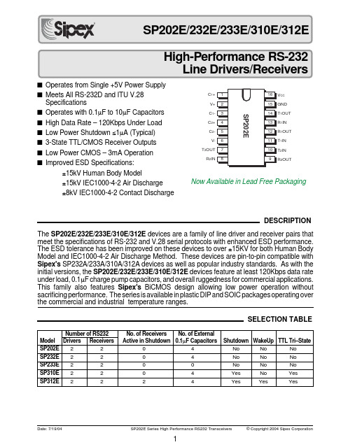
■Operates from Single +5V Power Supply ■Meets All RS-232D and ITU V.28Specifications■Operates with 0.1µF to 10µF Capacitors ■High Data Rate – 120Kbps Under Load ■Low Power Shutdown ≤1µA (Typical)■3-State TTL/CMOS Receiver Outputs ■Low Power CMOS – 3mA Operation ■Improved ESD Specifications:±15kV Human Body Model±15kV IEC1000-4-2 Air Discharge ±8kV IEC1000-4-2 Contact DischargeNumber of RS232No. of Receivers No. of ExternalModel Drivers Receivers Active in Shutdown 0.1µF CapacitorsShutdown WakeUp TTL Tri–StateSP202E 220 4No No No SP232E 220 4No No No SP233E 220 0No No No SP310E 220 4Yes No Yes SP312E222 4Yes Yes YesDESCRIPTIONSELECTION TABLEThe SP202E/232E/233E/310E/312E devices are a family of line driver and receiver pairs that meet the specifications of RS-232 and V.28 serial protocols with enhanced ESD performance.The ESD tolerance has been improved on these devices to over ±15KV for both Human Body Model and IEC1000-4-2 Air Discharge Method. These devices are pin-to-pin compatible withSipex's SP232A/233A/310A/312A devices as well as popular industry standards. As with the initial versions, the SP202E/232E/233E/310E/312E devices feature at least 120Kbps data rate under load, 0.1µF charge pump capacitors, and overall ruggedness for commercial applications.This family also features Sipex's BiCMOS design allowing low power operation without sacrificing performance. The series is available in plastic DIP and SOIC packages operating over the commercial and industrial temperature ranges.CC 1OUT 1IN 1OUT 1IN 2IN 2OUTC 1+V+C 1-C 2+C 2-V-T 2OUT R 2INNow Available in Lead Free PackagingThis is a stress rating only and functional operation of the device at these or any other conditions above those indicated in the operation sections of this specification is not implied. Exposure to absolute maximum rating conditions for extended periods of time may affect reliability.V cc .................................................................................................................................................................+6V V +....................................................................................................................(Vcc-0.3V) to +11.0V V -............................................................................................................................................................-11.0V Input VoltagesT IN .........................................................................................................................-0.3 to (Vcc +0.3V)R IN ............................................................................................................................................................±15V Output VoltagesT OUT ....................................................................................................(V+, +0.3V) to (V-, -0.3V)R OUT ................................................................................................................-0.3V to (Vcc +0.3V)Short Circuit DurationT OUT .........................................................................................................................................ContinuousV CC =+5V ±10%; 0.1µF charge pump capacitors; T MIN to T MAX unless otherwise noted.ELECTRICAL CHARACTERISTICSPlastic DIP ..........................................................................375mW (derate 7mW/°C above +70°C)Small Outline ......................................................................375mW (derate 7mW/°C above +70°C)ABSOLUTE MAXIMUM RATINGSPERFORMANCE CURVES-55-400257085125Temperature (°C)051015202530V CC = 6VV CC = 5VV CC = 4VV CC = 3VI C C (m A )05101520Load Current (mA)681012V + (V o l t s )24V CC = 5V V CC = 4VV CC = 6V253035402468101214Load Current (mA)V – V o l t a g e (V o l t s )-3-4-5-6-7-8-9-10-11V CC = 6VV CC = 5VV CC = 4V2OUT 2IN 2OUT 2-2+1–1+2+2–T 2IN T 1IN R 1OUT R 1IN T 1OUT GND V CC V+GNDV–CC 1OUT 1IN 1OUT 1IN 2IN 2OUTC 1+V+C 1-C 2+C 2-V-T 2OUT R 2INT CC 1OUT 1IN 1OUT 1IN 2IN 2OUTNC *C 1+V+C 1-C 2+C 2-V-T 2OUT R 2INCC 1OUT 1IN 1OUT 1IN 2IN 2OUTC 1+V+C 1-C 2+C 2-V-T 2OUT R 2IN* N.C. for SP310E_A, EN for SP312E_APINOUTS4.54.755.0 5.25 5.5V CC (Volts)5.06.57.07.58.08.59.0Load current = 0mA T A = 25°CV O H (V o l t s )5.56.0FEATURES…The SP202E/232E/233E/310E/312E devices are a family of line driver and receiver pairs that meet the specifications of RS-232 and V.28 serial protocols with enhanced ESD perfor-mance. The ESD tolerance has been improved on these devices to over ±15KV for both Human Body Model and IEC1000-4-2 Air Discharge Method. These devices are pin-to-pin compat-ible with Sipex's232A/233A/310A/312A devices as well as popular industry standards. As with the initial versions, the SP202E/232E/ 233E/310E/312E devices feature10V/µs slew rate, 120Kbps data rate under load, 0.1µF charge pump capacitors, overall ruggedness for commercial applications, and increased drive current for longer and more flexible cable configurations. This family also features Sipex's BiCMOS design allowing low power operation without sacrificing performance.The SP202E/232E/233E/310E/312E devices have internal charge pump voltage converters which allow them to operate from a single +5V supply. The charge pumps will operate with polarized or non-polarized capacitors ranging from 0.1 to 10 µF and will generate the ±6V needed to generate the RS-232 output levels. Both meet all EIA RS-232 and ITU V.28 specifications.The SP310E provides identical features as the SP232E with a single control line which simultaneously shuts down the internal DC/DC converter and puts all transmitter and receiver outputs into a high impedance state. The SP312E is identical to the SP310E with separate tri-state and shutdown control lines.THEORY OF OPERATIONThe SP232E,SP233E,SP310E and SP312E devices are made up of three basic circuit blocks –1) a driver/transmitter, 2) a receiver and 3) a charge pump. Each block is described below.Driver/TransmitterThe drivers are inverting transmitters, which ac-cept TTL or CMOS inputs and output the RS-232 signals with an inverted sense relative to the input logic levels. Typically the RS-232output voltage swing is ±6V. Even under worst case loading conditions of 3kOhms and 2500pF, the output is guaranteed to be ±5V, which is consistent with the RS-232 standard specifications. The transmitter outputs are protected against infinite short-circuits to ground without degradation in reliability.Figure 1. Typical Circuit using the SP202E or SP232E.The instantaneous slew rate of the transmitteroutput is internally limited to a maximum of 30V/µs in order to meet the standards [EIA RS-232-D 2.1.7, Paragraph (5)]. However, the transition re-gion slew rate of these enhanced products is typi-cally 10V/µs. The smooth transition of the loaded output from V OL to V OH clearly meets the mono-tonicity requirements of the standard [EIA RS-232-D 2.1.7, Paragraphs (1) & (2)].ReceiversThe receivers convert RS-232 input signals to inverted TTL signals. Since the input is usually from a transmission line, where long cable lengthsand system interference can degrade the signal, the inputs have a typical hysteresis margin of 500mV.This ensures that the receiver is virtually immune to noisy transmission lines.The input thresholds are 0.8V minimum and 2.4V maximum, again well within the ±3V RS-232requirements. The receiver inputs are also pro-tected against voltages up to ±15V. Should an input be left unconnected, a 5KOhm pulldown resistor to ground will commit the output of the receiver to a high state.Figure 2. Typical Circuits using the SP233ECP and SP233ECTFigure 3. Typical Circuits using the SP310E and SP312EFigure 4. Charge Pump — Phase 1Figure 5. Charge Pump — Phase 2In actual system applications, it is quite possible for signals to be applied to the receiver inputs before power is applied to the receiver circuitry.This occurs, for example, when a PC user attempts to print, only to realize the printer wasn’t turned on.In this case an RS-232 signal from the PC will appear on the receiver input at the printer. When the printer power is turned on, the receiver will operate normally. All of these enhanced devices are fully protected.Charge PumpThe charge pump is a Sipex –patented design (5,306,954) and uses a unique approach com-pared to older less–efficient designs. The charge pump still requires four external capacitors, but uses a four–phase voltage shifting technique to attain symmetrical power supplies. There is a free–running oscillator that controls the four phases of the voltage shifting. A description of each phase follows.Phase 1— V SS charge storage —During this phase of the clock cycle, the positive side of capacitors C 1 and C 2 are initially charged to +5V. C l + is then switched to ground and the charge in C 1– is transferred to C 2–. Since C 2+ is connected to +5V, the voltage potential across capacitor C 2 is now 10V.Phase 2— V SS transfer — Phase two of the clock con-nects the negative terminal of C 2 to the V SS storage capacitor and the positive terminal of C 2to ground, and transfers the generated –l0V to C 3. Simultaneously, the positive side of capaci-tor C 1 is switched to +5V and the negative side is connected to ground.Phase 3— V DD charge storage — The third phase of the clock is identical to the first phase — the charge transferred in C 1 produces –5V in the negative terminal of C 1, which is applied to the negative side of capacitor C 2. Since C 2+ is at +5V, the voltage potential across C 2 is l0V.Phase 4— V DD transfer — The fourth phase of the clock connects the negative terminal of C 2 to ground,and transfers the generated l0V across C 2 to C 4,the V DD storage capacitor. Again, simultaneously with this, the positive side of capacitor C 1 is switched to +5V and the negative side is con-nected to ground, and the cycle begins again.Since both V + and V – are separately generated from V CC ; in a no–load condition V + and V – willFigure 6. Charge Pump Waveforms+10Va) C 2+GND GNDb) C 2––10VFigure 7. Charge Pump — Phase 3Figure 8. Charge Pump — Phase 4be symmetrical. Older charge pump approaches that generate V – from V + will show a decrease in the magnitude of V – compared to V + due to the inherent inefficiencies in the design.The clock rate for the charge pump typically operates at 15kHz. The external capacitors can be as low as 0.1µF with a 16V breakdown voltage rating.Shutdown (SD) and Enable (EN) for the SP310E and SP312EBoth the SP310E and SP312E have a shutdown/standby mode to conserve power in battery-pow-ered systems. To activate the shutdown mode,which stops the operation of the charge pump, a logic “0” is applied to the appropriate control line.For the SP310E , this control line is ON/OFF (pin 18). Activating the shutdown mode also puts theSP310E transmitter and receiver outputs in a high impedance condition (tri-stated). The shutdown mode is controlled on the SP312E by a logic “0”on the SHUTDOWN control line (pin 18); this also puts the transmitter outputs in a tri–state mode. The receiver outputs can be tri–stated separately during normal operation or shutdown by a logic “1” on the ENABLE line (pin 1).Wake–Up Feature for the SP312EThe SP312E has a wake–up feature that keeps all the receivers in an enabled state when the device is in the shutdown mode. Table 1 defines the truth table for the wake–up function.With only the receivers activated, the SP312E typically draws less than 5µA supply current. In the case of a modem interfaced to a computer in power down mode, the Ring Indicator (RI) signal from the modem would be used to "wake up" the computer, allowing it to accept data transmission.After the ring indicator signal has propagated through the SP312E receiver, it can be used to trigger the power management circuitry of the computer to power up the microprocessor, and bring the SD pin of the SP312E to a logic high, taking it out of the shutdown mode. The receiver propagation delay is typically 1µs. The enable time for V+ and V– is typically 2ms. After V+ and V– have settled to their final values, a signal can be sent back to the modem on the data terminal ready (DTR) pin signifying that the computer is ready to accept and transmit data.Pin Strapping for the SP233ECTThe SP233E packaged in the 20–pin SOIC pack-age (SP233ECT) has a slightly different pinout than the SP233E in other package configurations. To operate properly, the following pairs of pins must be externally wired together:the two V– pins (pins 10 and 17)the two C2+ pins (pins 12 and 15)the two C2– pins (pins 11 and 16)All other connections, features, functions and performance are identical to the SP233E as specified elsewhere in this data sheet.ESD TOLERANCEThe SP202E/232E/233E/310E/312E devices incorporates ruggedized ESD cells on all driver output and receiver input pins. The ESD struc-ture is improved over our previous family for more rugged applications and environments sen-sitive to electro-static discharges and associated transients. The improved ESD tolerance is at least ±15KV without damage nor latch-up. There are different methods of ESD testing applied:a) MIL-STD-883, Method 3015.7b) IEC1000-4-2 Air-Dischargec) IEC1000-4-2 Direct ContactThe Human Body Model has been the generally accepted ESD testing method for semiconductors. This method is also specified in MIL-STD-883, Method 3015.7 for ESD testing. The premise of this ESD test is to simulate the human body’s potential to store electro-static energy and discharge it to an integrated circuit. The simulation is performed by using a test model as shown in Figure 9. This method will test the IC’s capability to withstand an ESD transient during normal handling such as in manufacturing areas where the ICs tend to be handled frequently.The IEC-1000-4-2, formerly IEC801-2, is generally used for testing ESD on equipment and systems. For system manufacturers, they must guarantee a certain amount of ESD protection since the system itself is exposed to the outside environment and human presence. The premiseTable 1. Wake-up Function Truth Table.Figure 9. ESD Test Circuit for Human Body ModelFigure 10. ESD Test Circuit for IEC1000-4-2with IEC1000-4-2 is that the system is required to withstand an amount of static electricity when ESD is applied to points and surfaces of the equipment that are accessible to personnel during normal usage. The transceiver IC receives most of the ESD current when the ESD source is applied to the connector pins. The test circuit for IEC1000-4-2 is shown on Figure 10. There are two methods within IEC1000-4-2, the Air Discharge method and the Contact Discharge method.With the Air Discharge Method, an ESD voltage is applied to the equipment under test (EUT)through air. This simulates an electrically charged person ready to connect a cable onto the rear of the system only to find an unpleasant zap just before the person touches the back panel. The high energy potential on the person discharges through an arcing path to the rear panel of the system before he or she even touches the system.This energy, whether discharged directly or through air, is predominantly a function of theSP202E HUMAN BODY IEC1000-4-2FamilyMODEL Air Discharge Direct Contact LevelDriver Outputs ±15kV ±15kV ±8kV 4Receiver Inputs ±15kV±15kV±8kV4Figure 11. ESD Test Waveform for IEC1000-4-2t=0nst=30ns0A15A30At ➙i ➙Table 2. Transceiver ESD Tolerance Levelsdischarge current rather than the discharge voltage. Variables with an air discharge such as approach speed of the object carrying the ESD potential to the system and humidity will tend to change the discharge current. For example, the rise time of the discharge current varies with the approach speed.The Contact Discharge Method applies the ESD current directly to the EUT. This method was devised to reduce the unpredictability of the ESD arc. The discharge current rise time is constant since the energy is directly transferred without the air-gap arc. In situations such as hand held systems, the ESD charge can be directlydischarged to the equipment from a person already holding the equipment. The current is transferred on to the keypad or the serial port of the equipment directly and then travels through the PCB and finally to the IC.The circuit models in Figures 9 and 10 represent the typical ESD testing circuit used for all three methods. The C S is initially charged with the DC power supply when the first switch (SW1) is on.Now that the capacitor is charged, the second switch (SW2) is on while SW1 switches off. The voltage stored in the capacitor is then applied through R S , the current limiting resistor, onto the device under test (DUT). In ESD tests, the SW2switch is pulsed so that the device under test receives a duration of voltage.For the Human Body Model, the current limiting resistor (R S ) and the source capacitor (C S ) are 1.5k Ω an 100pF, respectively. For IEC-1000-4-2, the current limiting resistor (R S ) and the source capacitor (C S ) are 330Ω an 150pF, respectively.The higher C S value and lower R S value in the IEC1000-4-2 model are more stringent than the Human Body Model. The larger storage capacitor injects a higher voltage to the test point when SW2 is switched on. The lower current limiting resistor increases the current charge onto the test point.D 2x 2E1A1DETAIL A- - 2.00.05 - -Dimensions in (mm)20 PIN SSOP JEDEC MO-150(AE) V ariation1.65 1.75 1.850.22 - 0.380.09 - 0.250.55 0.75 0.950º 4º 8ºA A1A2b c D E E1L L1ØMIN NOM MAX 7.407.808.205.005.305.601.25 REF6.907.207.5020 PIN SSOPPACKAGE: 20 PIN SSOPPACKAGE: 16 PIN NSOIC16 PIN NSOICPACKAGE: 16 PIN WSOIC16 PIN SOIC WIDE- - .210.015 -Dimensions in inches 18 PIN PDIP JEDEC MS-001(AC) V ariation.115 .130 .195 .014 .018 .022.045 .060 .070.240 .250 .280A A1A2b c D1E E1e eA eB .115 .130 .150LMIN NOM MAX b2b3.030 .039 .045D .008.010.014.880.900.920.005.300.310.325.100 BSC .300 BSC .430-----18 pin PDIPPACKAGE: 18 PIN PDIPPart Number Temperature Range Topmark Package SP202ECN.............................0°C to +70°C.................................SP202ECN........................................................................16–pin NSOIC SP202ECN/TR.......................0°C to +70°C.................................SP202ECN........................................................................16–pin NSOIC SP202ECP.............................0°C to +70°C.................................SP202ECP.........................................................................16–pin PDIP SP202ECT.............................0°C to +70°C.................................SP202ECT.........................................................................16–pin WSOIC SP202ECT/TR.......................0°C to +70°C.................................SP202ECT.........................................................................16–pin WSOIC SP202EEN..........................–40°C to +85°C................................SP202EEN.........................................................................16–pin NSOIC SP202EEN/TR....................–40°C to +85°C................................SP202EEN.........................................................................16–pin NSOIC SP202EEP..........................–40°C to +85°C................................SP202EEP.........................................................................16–pin PDIP SP202EET..........................–40°C to +85°C................................SP202EET..........................................................................16–pin WSOIC SP202EET/TR.....................–40°C to +85°C................................SP202EET..........................................................................16–pin WSOIC SP232ECN.............................0°C to +70°C................................SP232ECN..........................................................................16–pin NSOIC SP232ECN/TR.......................0°C to +70°C................................SP232ECN..........................................................................16–pin NSOIC SP232ECP.............................0°C to +70°C.................................SP232ECP.........................................................................16–pin PDIP SP232ECT.............................0°C to +70°C.................................SP232ECT..........................................................................16–pin WSOIC SP232ECT/TR.......................0°C to +70°C.................................SP232ECT..........................................................................16–pin WSOIC SP232EEN..........................–40°C to +85°C................................SP232EEN..........................................................................16–pin NSOIC SP232EEN/TR....................–40°C to +85°C................................SP232EEN..........................................................................16–pin NSOIC SP232EEP..........................–40°C to +85°C................................SP232EEP..........................................................................16–pin PDIP SP232EET..........................–40°C to +85°C................................SP232EET...........................................................................16–pin WSOIC SP232EET/TR.....................–40°C to +85°C................................SP232EET...........................................................................16–pin WSOIC SP233ECT............................0°C to +70°C.................................SP233ECT...........................................................................20–pin WSOIC SP233ECT/TR......................0°C to +70°C.................................SP233ECT...........................................................................20–pin WSOIC SP233EET..........................–40°C to +85°C................................SP233EET...........................................................................20–pin WSOIC SP233EET/TR.....................–40°C to +85°C................................SP233EET...........................................................................20–pin WSOIC SP310ECP............................0°C to +70°C.................................SP310ECP.........................................................................18–pin PDIP SP310ECT............................0°C to +70°C.................................SP310ECT..........................................................................18–pin WSOIC SP310ECT/TR......................0°C to +70°C.................................SP310ECT..........................................................................18–pin WSOIC SP310ECA............................0°C to +70°C.................................SP310ECA..........................................................................20–pin SSOP SP310ECA/TR......................0°C to +70°C.................................SP310ECA..........................................................................20–pin SSOP SP310EEP..........................–40°C to +85°C................................SP310EEP..........................................................................18–pin PDIP SP310EET..........................–40°C to +85°C................................SP310EET...........................................................................18–pin WSOIC SP310EET/TR.....................–40°C to +85°C................................SP310EET...........................................................................18–pin WSOIC SP310EEA..........................–40°C to +85°C................................SP310EEA...........................................................................20–pin SSOP SP310EEA/TR.....................–40°C to +85°C................................SP310EEA...........................................................................20–pin SSOP SP312ECP............................0°C to +70°C.................................SP312ECP..........................................................................18–pin PDIP SP312ECT............................0°C to +70°C.................................SP312ECT...........................................................................18–pin WSOIC SP312ECT/TR......................0°C to +70°C.................................SP312ECT...........................................................................18–pin WSOIC SP312ECA............................0°C to +70°C.................................SP312ECA...........................................................................20–pin SSOP SP312ECA/TR......................0°C to +70°C.................................SP312ECA...........................................................................20–pin SSOP SP312EEP..........................–40°C to +85°C................................SP312EEP...........................................................................18–pin PDIP SP312EET..........................–40°C to +85°C................................SP312EET............................................................................18–pin WSOIC SP312EET/TR.....................–40°C to +85°C................................SP312EET............................................................................18–pin WSOIC SP312EEA..........................–40°C to +85°C................................SP312EEA............................................................................20–pin SSOP SP312EEA/TR.....................–40°C to +85°C................................SP312EEA............................................................................20–pin SSOPapplication or use of any product or circuit described hereing; neither does it convey any license under its patent rights nor the rights of others.Available in lead free packaging. To order add "-L" suffix to part number.Example: SP312EEA/TR = standard; SP312EEA-L/TR = lead free /TR = Tape and ReelPack quantity is 1,500 for SSOP or WSOIC and 2,500 for NSOIC.Sipex Corporation Headquarters and Sales Office233 South Hillview Drive Milpitas, CA 95035TEL: (408) 934-7500FAX: (408) 935-7600ORDERING INFORMATIONREVISION HISTORY。
动作经济原则事例

同一方向(不适当)
对称方向(适当)
IE Dept. TEL:84878978-308
IE 论坛
动作经济基本原则Ⅱ——同时进行动作
一、关于动作方法——两手同时反向对称方向移动
例2:根据海棉板的利用组装螺栓、螺母电阻实行两手同时化 改善前:左手拿电阻右手1个个抓取螺母送至 手边两面组装用右手横向运送组装品放置
IE 方秀兰
(幻灯片观看放映版)
IE Dept. TEL: 84878978-308 IE Dept. TEL: 84878978-308 Email: Email:DCLi@ DCLi@ IE Dept. TEL: 84878978-308
例2:材料的刮伤检查的两手同时化 改善前:每一个拿想检查 改善后:每2个拿起检查
IE Dept. TEL:84878978-308
IE 论坛
动作经济基本原则Ⅱ——同时进行动作
一、关于动作方法——两手同时反向对称方向移动
容 易 作 业 的 分 类 例1:根据变更浆糊的直接贴付方式使之两手同时化 改善前:左手从箱内拿出本体右手用笔涂浆糊于本体 上放置涂浆糊的笔于器皿上从箱内拿出盖子两手按压 左手放入完成品至箱内 改善后:左右手同时从箱里拿出盖子装入 治具上两手同时从箱内拿出本体同时涂浆 糊同时压入盖盖同时将完成品放入箱入 手移动的方法
二、关于作业场所—作业区域在没有阻碍范围内使之变窄
例1:由于变更部品放置 场所使动作距离缩短 改善前:作业员两边横向 的台面上放置A、B部品 改善后:设置作业台,使 作业员和传送带靠近部品 都放置于作业台上面
IE Dept. TEL:84878978-308
IE 论坛
动作经济基本原则Ⅰ——作业场所
二、作业场所—材料和工具放置于作业员前方固定场所
三星SITOP双重冗余模块SITOP PSE202U说明书

-25 ... +60 °C with natural convection -40 ... +85 °C -40 ... +85 °C Climate class 3K3, 5 … 95% no condensation
screw-type terminals
● top ● bottom ● left
96.6 % 34 1.5 W
yes, SELV acc. to EN 60950-1 (relay contact) Class III IP20
Yes cULus-Listed (UL 508, CSA C22.2 No. 107.1), File E197259 IECEx Ex nA nC IIC T4 Gc; ATEX (EX) II 3G Ex nAC IIC T4; cCSAus (CSA C22.2 No. 213, ANSI/ISA-12.12.01) Class I, Div. 2, Group ABCD, T4 No ABS, DNV GL
0 mm 0.5 kg Yes
Snaps onto DIN rail EN 60715 35x7.5/15 6 471 654 h Specifications at rated input voltage and ambient temperature +25 °C (unless otherwise specified)
Signaling
Rated current value Iout rated Current range
● Note
6EP1961-3BA21 Page 1/3
DC voltage
3300ICP_52系列IP话机使用手册_ed00

Mitel 3300 ICP53系列IP话机使用手册版本:00目录1综述 (4)2使用介绍 (5)2.15212IP话机 (5)2.25224IP话机 (6)2.3设置话机功能 (7)2.4定义功能键 (7)2.5显示一个功能键的信息 (7)2.6铃音调节 (8)2.7手柄收听音量调节 (8)2.8扬声器音量调节 (8)2.9显示屏对比度调节 (8)2.10语言设置 (8)3基本功能 (9)3.1拨打电话 (9)3.2应答来电 (9)3.3重拨 (9)3.4保存及重拨号码 (9)3.5速拨键 (9)3.6个人速拨号码 (10)3.7H OLD(保持) (10)3.8静音 (10)3.9呼叫转接 (11)3.10呼叫转移 (11)3.11结束一组呼叫转移 (12)3.12呼叫转移链跳过某话机 (13)3.13A UTO ANSWER(自动接听来电) (13)3.14C ALLBACK(回叫) (13)3.15S WAP (穿梭通话) (13)3.16三方会议 (13)3.17拆分三方会议 (14)4高级功能 (15)4.1组内代接 (15)4.2C AMP ON(等待) (15)4.3P ICK UP(代接) (15)4.4DND(免打扰) (15)4.5C ALL HISTORY (16)4.6录音 (16)4.7M USIC(音乐) (17)4.8H OT D ESKING (17)5特色功能(仅5224 IP话机) (19)5.1P HONEBOOK(按姓名拨号) (19)5.2R EMINDER(叫醒) (19)1综述本文档适用于Mitel 3300 ICP系列中52系列IP话机(5212,5224)的使用。
若无特殊注明,该文档中描述的操作步骤均适用于这两种IP话机。
本文档仅供参考。
如需了解更详细信息,请参见敏迪的技术文档。
本文档中的内容若有修改,恕不另行通知。
文档的更新状态,请登陆公司网站查询:2使用介绍2.15212 IP话机性能特点:→ 2 行, 20 字符白色背光液晶显示屏→支持双模操作 - SIP 和MiNET→双网口,10/100 BaseT交换式以太网口→12 个可编程带LED支持灯功能键→10 个固定功能键,SuperKey –可对可编程键快速编程→支持半双功免提通话,支持摘机广播/免提应答功能→支持标准POE供电标准802.3af→支持WLAN和千兆机座2.25224 IP话机性能特点:→ 2 行, 20 字符白色背光液晶显示屏→支持双模操作 - SIP 和MiNET→双网口,10/100 BaseT交换式以太网口→24 个可编程带LED支持灯功能键→10 个固定功能键,SuperKey –可对可编程键快速编程→3个软功能键→支持全双功免提通话,支持摘机广播/免提应答功能→支持标准POE供电标准802.3af→可连接会议单元,PKM,LIM,支持WLAN和千兆机座2.3设置话机功能1、按2、按no往下翻页,直到显示我们想要的功能3、按yes4、选择一个功能5、根据屏幕提示开启或关闭相应的功能6、按退出主要选项:Phone book,forward,personal keys,wake up, dnd, auto answer(5224 only), ringer adjust,language2.4定义功能键1、按2、按no往下翻页,直到显示“personal keys”3、按yes4、选择一个功能键。
GMRC Surge Guide Line

GMRC Guideline – Release Version 4.3 Application Guideline for Centrifugal Compressor Surge Control Systems
APPLICATION GUIDELINE FOR CENTRIFUGAL COMPRESSOR SURGE CONTROL SYSTEMS
RELEASE VERSION 4.3
April 2008 Gas Machinery Research Council Southwest Research Insti Release Version 4.3 Application Guideline for Centrifugal Compressor Surge Control Systems
The Gas Machinery Research Council provides its member companies and industry with the benefits of an applied research and technology program directed toward improving reliability and cost effectiveness of the design, construction and operation of mechanical and fluid systems. GMRC’s vision is to be a leading, financially self-sufficient, not-for-profit research corporation that provides focused, cost-effective technology and services for the global marketplace in the rapidly changing natural gas, oil and petrochemical industries.
- 1、下载文档前请自行甄别文档内容的完整性,平台不提供额外的编辑、内容补充、找答案等附加服务。
- 2、"仅部分预览"的文档,不可在线预览部分如存在完整性等问题,可反馈申请退款(可完整预览的文档不适用该条件!)。
- 3、如文档侵犯您的权益,请联系客服反馈,我们会尽快为您处理(人工客服工作时间:9:00-18:30)。
上海三花电气有限公司 组织结构图
总经理
副总经理
市场部
人事行政部
财务部
采购部
质保部
生产制造部
产品工程 部
物 料 供 应
生 产 车 间
制 造 工 艺
产 品 设 计
技 术 标 准
试 验 试 制
不断进取的管理团队
现有 硕士研究生:3 人 本科生:18人 大专生:10人
主要产品及生产能力
一、操纵机构:150万套/年(双班) 其中:手动操纵机构 电动操纵机构 自动操纵机构 110万套/年 30万套/年 10万套/年
策划
生产 GP12先期产品质量遏制 反馈,评估及整改措施 GP 9 按预定节拍生产
计划与确 定 项目
产品设计 与开发
工艺设计 与开发
产品及 工艺认证
反馈,评估及 整改措施
项目管理
STAGEGATE 1 - QUOTATION GATE STAGEGATE 2 - PROJECT LAUNCH GATE STAGEGATE 3 - PROTOTYPE VALIDATION GATE STAGEGATE 4 - DESIGN/COST VERIFICATION GATE STAGEGATE 5 - PRODUCTION READINESS GATE STAGEGATE 6 - STABLE PRODUCTION GATE
二、伺服机构:36万件/年 (双班)
质量方针
坚持以人为本 ,推动科技进步 强化质量管理 ,致力持续改进 提供优质产品 ,保证顾客满意
PV生产确认试验
上海三花产品质量先期策划 (APQP)
样件(OTS) DV设计验证 PPAP 投产SOP
产品审核
概念 形成/审批
项目审批
策划 产品设计与开发 工艺设计与开发 过程审核 产品及工艺认证
试验设备 2
振动试验台
振动试验台
伺服器性能
伺服器角度
控制面板检测
控制面板性能
试验设备 3
高低温试验箱
高温试验箱
万工显
寿命试验台
控制面板寿命试验台
最大扭矩试验台
试验设备 4
爱色丽SP64分光光度仪( 测试颜色L*La*Lb*值) 漆面耐磨耗试验机
颜色透光测试仪
试验设备 5
浪涌测试仪
体视视频成像仪
国内市场营销网络图
• • • • • • • • • • • • • 上海德尔福汽车空调系统有限 公司 空调国际(上海 )有限公司 上海威乐汽车空调有限公司 上汽通用五菱汽车股份有限公 司 麦克斯(保定)汽车空调有限 公司 一汽-杰克赛尔汽车空调有限 公司 天津三电汽车空调有限公司 上海恒安空调设备有限公司 上海加冷松芝汽车空调有限公 司 厦门建松电器有限公司 武汉申龙汽车空调有限公司 法雷奥汽车空调湖北有限公司 河南豫新汽车空调有限公司
VW Gol
控制面板与配套车型 1
M1 控制面板
华晨尊驰
华晨骏捷 M2 控制面板
Spark 控制面板
SGMW Spark
控制面板与配套车型 2
2000 型控制面板
Santana 2000
Santana 3000 GP4 控制面板
N200 控制面板
SGMW N200 鸿途
控制面板与配套车型 3
菲亚特控制面板
日产改进型控制面板
帕拉丁
N323 控制面板
海马福美来
普利马控制面板
海马普利马
控制面板与配套车型 7
昌河控制面板
昌河北斗星
昌河 6351 控制面板
昌河 6351 爱迪尔l
迪尔控制面板
长城迪尔
控制面板与配套车型 8
富康控制面板l
富康
高尔 高尔控制面板
杰士达控制面板
华普海尚
控制面板与配套车型 9
力帆控制面板
上海三花电气有限公司销售业绩
RMB Million Yuan
60 50 40 30 20 10 0 1.03 3.94 6.21 8.78 19.2 28.2630.28 34.3 53 48
1998 1999 2000 2001 2002 2003 2004 2005 2006 2007 Year
PDCA管理
① P(计划):确定目的、目标。确定未达成目的的体系、 方法。对事故防患于未然。 ② D(实施):实施。(包括教育培训) ③ C(结果的确认):与目标进行比较确认。 ④ A(处理):采取临时应急对策。进行解析,抓住真正的 原因,采取根本对策。实施标准化防止再发。
管理 改善
A C P D
1
2
3
4
5
6
PFD/PFMEA/PCP/作业指导书/操作者培训
顾客要求 顾客要求 关键特性识别 关键特性识别 KCDS KCDS 过程流程图 过程流程图 PFD PFD 过程失效模式 过程失效模式 PFMEA PFMEA
质量数据/ 质量数据/ 不断改进 不断改进
历史经验教训 历史经验教训 质量问题数据 质量问题数据
今后五年国内市场规划
BUSINESS STATUS 2006 D(MILs) 2007 D(MILs) 2008 D(MILs) 2009 D(MILs) 2010 D(MILs) 2011 D(MILs) 业务状况
Current In Develop ment Potential USD
维持管理
A C P D
改善目标
2003年12月通过ISO/TS16949-2002认证
质量体系认可证书
产品设计
产品正向设计 汽车主机厂提供详细需求及技术指标,而无 样机和图纸.其中包括与汽车主机厂同步开发 新车型的空调系统. 产品逆向设计 汽车主机厂提供样机但无细部的图纸
产品开发周期(项目授权批准~稳定生产)
14.00
3.76
3.30
3.04
2.74
2.70
2.54
现有的 开发中 的 潜在的 百万美 圆
1.17 4.92
2.68 0.71 6.69
2.71 2.71 8.46
2.79 5.21 10.73
3.07 6.22 11.99
3.26 6.66 12.45
12.00
10.00
8.00
Potential In Development Current
试验设备 6
热风回流焊机
老化试验室
控制面板生产线
控制面板性能检测设备
控制面板生产线
伺服器生产线
伺 服 器 性 能 检 测
6S 现场管理
6S 现场管理
6S 现场管理
6S 现场管理
谢谢!
2007. 11
WELCOME TO OUR COMPANY 欢迎莅临指导
上海三花电气有限公司简介
公司基本状况 公司成立:1998年 注册资金:RMB 18,000,000 总 资 产:RMB 40,000,000 公司面积:9,870 平方米 投 资 方:三花控股集团有限公司 70% • 上海汽车空调器厂 30% • 质量体系:ISO/TS16949, Dec 2003 • • • • •
派朗
菲亚特 05 控制面板
派力奥
庆铃 100P
庆铃 100P
控制面板与配套车型 4
R23 控制面板
爱丽舍
CK-1 控制面板
吉利 CK-1
LG-1 控制面板
吉利 LG-1
控制面板与配套车型 5
金杯阁瑞斯电动控制面板 金杯阁瑞斯
陆风电动控制面板
陆风风尚
庆铃140P控制面板
庆铃 140
控制面板与配套车型 6
过程控制计划 过程控制计划 PCP PCP 作业指导书 作业指导书 培训 培训 操作者/检验员 操作者/检验员
经验教训 经验教训 积累 积累
分级检查 分级检查
过程防错控制
•缺陷的根源
–被疏忽的过程 –工序错误 –错误的工序流程 –缺少零件 –错误的零件 –错误的工作基准 –误操作 –调整错误 –设备安装不当 –工具和夹具准备不当
手动操纵机构 电动操纵机构 自动操纵机构 伺服机构 9个月 12个月 12个月 6个月
结构设计:UG,PRO/E,CATIA
•
电气原理设计: PROTEL-SCH
电气设计:PROTEL99
控制系统:FreeScale Chip, C Language Programming
控制系统:Renesas Chip,C Language Programming
力帆 520
IVECO 后控
IVECO IVECO 前控
控制面板与配套车型 10
MG-3 控制面板
MG 名爵
Liana 控制面板 Liana
瑞风 前后 控制面板
江淮瑞风
自动空调控制面板
帕拉丁
金杯阁瑞斯控制面板
金杯阁瑞斯
试验设备 1
高低温冲击试验箱
潮湿温度试验箱
主要客户
三花集团国际营销网络
Hamburg Pusan Osaka Columbus/OH
Bangkok
Sales Office China Warehouse Sales Office Warehouse Manufacture plant 7 7 6 US / N. America 1 1 Japan 1 1 Thailand 1 1 1 Malaysia Korea 1 1
导光光纤的设计:导光光路的分析
光路分析
导光面强度分析
导光分析
SGM 308
与泛亚同步开发SGM308控制头、制定SOR。
供应商的管理
上海三花已经形成了一套比较完整的供应体系。上海三 花现有38家长期合作供应商,其中32家已通过ISO9001和 ISO/TS16949系统认证,其中部分供应商为上海大众、上海 通用、一汽大众、神龙富康等大型主机厂的供货商。 随着市场竞争日益激烈,上海三花正在进行供应商体系 的评估和供应链的整合,以提高供应商的水平和能力。新开 发产品已经实行APQP(先期产品质量策划)、PPAP等认 证手段,以保证新品开发的进度和质量