3C16832中文资料
TDA16831中文资料

Off-line SMPS Controller with 600 V Sense CoolMOS on BoardTDA16831-4Preliminary Data CoolSETOverview Features•PWM controller + sense CoolMOS attached in one compact package •600 V avalanche rugged CoolMOS•Typical R DSon = 0.5 ... 3.5 Ω at T j = 25 °C •Only 4 active Pins•Standard DIP-8 Package for Output Power ≤40 W•Only few external components required •Low start up current •Current mode control•Input Undervoltage Lockout •Max. Duty Cycle limitation •Thermal Shutdown•Modulated Gate Drive for low EMIType Ordering Code Package TDA 16831Q67000-A9420P-DIP-8-6TDA 16832Q67000-A9422P-DIP-8-6TDA 16833Q67000-A9389P-DIP-8-6TDA 16834samples P-DIP-8-6TDA 16831G Q67000-A9421P-DSO-14-11TDA 16832G Q67000-A9423P-DSO-14-11TDA 16833GQ67000-A9419P-DSO-14-11Device Output Power Range/Required Heatsink1)Output Power Range/ Required Heatsink1)Vin= 85-270 VAC V in = 190-265 VAC TDA1683110 W / no heatsink10 W / no heatsink TDA1683220 W / 6 cm220 W / no heatsink TDA1683330 W / 3 cm240 W / no heatsink TDA1683440 W / 3 cm240 W / no heatsink TDA16831G10 W / no heatsink10 W / no heatsink TDA16832G20 W / 8 cm220 W / no heatsink TDA16833G20 W / no heatsink40 W / 3 cm21)TA= 70 °CPin ConfigurationsFigure1TDA16831/2/3/4P-DIP-8-6 for Applications with P out≤ 40 W: TDA16831/2/3/4 Pin Symbol Function1N.C.Not Connected2FB PWM Feedback Input3N.C.Not Connected4D600 V Drain CoolMOS5D600 V Drain CoolMOS6N.C.Not Connected7V CC PWM Supply Voltage8GND PWM GND and Source of CoolMOSFigure2TDA16831G/2G/3GP-DSO-14-11 for Applications with P out ≤ 20 W: TDA16831G/2G/3G Pin Symbol Function1GND PWM GND and CoolMOS Source2FB PWM Feedback Input3N.C.Not Connected4N.C.Not Connected5, 6, 7D600 V Drain CoolMOS8, 9, 10D600 V Drain CoolMOS11N.C.Not Connected12N.C.Not Connected13V CC PWM Supply Voltage14GND PWM GND and Source of CoolMOSData Sheet 5 1999-12-10Figure3Block DiagramTDA 16831-4Circuit DescriptionThe TDA 16831-4 is a current mode pulse width modulator with integrated sense CoolMOS transistor. It fulfills the requirements of minimum external control circuitry for a flyback application.Current mode control means that the current through the MOS transistor is compared with a reference signal derived from the output voltage of the flyback application. The result of that comparison determines the on time of the MOS transistor.To minimize external circuitry the sense resistor which gives information about MOS current is integrated. The oscillator resistor and capacitor which determine the switching frequency are integrated, too. Special efforts have been made to compensate temperature dependency and to minimize tolerances of this resistor. The circuit in detail: (see Figure3)Start Up Circuit (uvlo)Uvlo is monitoring the external supply voltage V CC. When V CC is exceeding the on threshold V CCH = 12 V, the bandgap, the bias circuit and the soft start circuit are switched on. When V CC is falling below the off-threshold V CCL = 9 V the circuit is switched off. During start up the current consumption is about 30 µA.Bandgap (bg)The bandgap generates an internal very accurate reference voltage of 5.5 V to supply the internal circuits.Current Source (bias)The bias circuit provides the internal circuits with constant current.Oscillator (osc)The oscillator is generating a frequency twice the switching frequency fswitch=100kHz. Resistor, capacitor and current source which determine the frequency are integrated. The charging and discharging current of the implemented oscillator capacitor is internally trimmed, in order to achieve a very accurate switching frequency. Temperature coefficient of switching frequency is very low ( see page 19).Divider Flip Flop (tff)Tff is a flip flop which divides the oscillator frequency by one half to create the switching frequency. The maximum duty cycle is set to Dmax=0.5.Current Sense Amplifier (pwmop)The positive input of the pwmop is applied to the internal sense resistor. With the internal sense resistor (R sense) the sensed current coming from the CoolMOS is converted into a sense voltage. The sense voltage is amplified with a gain of 32dB. The amplified sense voltage is connected to the negative input of the pwm comparator. Each time when the CoolMOS transistor is switched on, a current spike is superposed to the true current information. To eliminate this current spike the sense voltage is smoothed via an internal resistor capacitor network with a time constant ofTd1= 100 ns. This is the first leading edge blanking and only a small spike is left. To reduce this small spike the current sense amplifier is creating a virtual ramp at the output. This is done by a second resistor capacitor network with T d2 = 100 ns and an op-offset of 0.8 V which is seen at the output of the amplifier. When gate drive isswitched off the output capacitor is discharged via pulse signal pwmpls. The oscillator signal slogpwm sets the RS-flip-flop. The gate drive circuit is switched on,when capacitor voltage exceeds the internal threshold of 0.4 V. This leads to a linear ramp, which is created by the output of the amplifier. Therefore duty cycle of 0% is possible. The amplifier is compensated through an internal compen-sation network.The transfer function of the amplifier can be described asthe step response is described withComparator (pwmcomp)The comparator pwmcomp compares theamplified current signal pwmrmp of the CoolMOS with the reference signal pwmin.Pwmin is created by an external optocoupler or external transistor and gives the information of the feedback circuitry. When the pwmrmp exceeds the reference signal pwmin the comparator switches the CoolMOS off.Logic (logpwm)The logic logpwm comprises a RS-flip-flop and a NAND-gate. The NAND-gate insures that CoolMOS transistor is only switched on when sosta is on and pwmin has exceeded minimum threshold and pwmin is below pwmrmp and currentshutdown is off and tempshutdown is off and tff sets the starting impulse.CoolMOS transistor is switched off when pwmrmp exceeds pwmin or duty cycle exceeds 0.5 or pwmcs exceeds I max or silicium temperature exceeds T max or uvlo is going below threshold. The RS flip flop ensures that with every frequency period only one switch on can occur (double pulse suppression).Gate Drive (gtdrv)Gtdrv is the driver circuit for the CoolMOS and is optimized to minimize EMI influences and to provide high circuit efficiency. This is done by smoothing the switch on slope when reaching the CoolMOS threshold. Leading switch on spike is minimized then. When CoolMOS is witched off, the falling slope of the gate driver is slowed down when reaching 2V.So an overshoot below ground can't occur.Also gate drive circuit is designed to eliminate cross conduction of the output stage.Current Shut Down (cssd)Current shut down circuit switches the CoolMOS immediately off when the sense current is exceeding an internal threshold of 100 mV at R sense .Vo V i -----K i p 1T p ×+()×----------------------------------- p ;j ω==V o V i K i ×=t on T –T e-t on T---------×+èç÷æö×K i 40t on -----=T 850 ns=Tempshutdown (tsd)Tempshutdown switches the CoolMOS off when junction temperature of the PWM controller is exceeding an internal threshold.Figure4Signal DiagramElectrical Characteristics 1) Be aware that V CC capacitor is discharged before IC is plugged into the application board.2)Power dissipation should be observed.Absolute Maximum Ratings Parameter Symbol Limit Values Unit Remarks min.max.Supply Voltage Supply + Zener Current V CC I CCZ –0.30V Z20V mA Zener Voltage 1) page 11Beware of P max 2)Drain Source Voltage Avalanche Current V DS I AC 600I csthmaxVt = 100 nsVoltage at FB V FB –0.3 5.5V Junction Temperature T j –40150°C Storage TemperatureT stg –50150°CThermal Resistance System-AirR thSA R thSA90125K/W K/W P-DIP-8-6P-DSO-14-11Operating Range Parameter SymbolLimit Values Unit Remarks min.max.Supply Voltage V CC V CCHV ZV Junction TemperatureT j–25120°CSupply Section-25 °C < T j < 120 °C, V CC = 15 V ParameterSymbolLimit Values Unit Test Conditionsmin.typ.max.Quiescent Current Supply Current Active Supply Current Active Supply Current ActiveI CCL I CCHA I CCHA I CCHA 254.5678067.58.5µAmA mA mATDA 16831/2/G TDA 16833/G TDA 16834V CC Turn-On Threshold V CC Turn-Off Threshold V CC Turn-On/Off Hysteresis V CC Zener ClampV CCH V CCL V CCHY V Z 8.516129317.512.519V V V V Controller Thermal Shutdown Thermal HysteresisT jSD T jHy1201352150°C °CTDA 16831/2/3/G/4Oscillator Section-25 °C < T j < 120 °C, V CC = 15 V Parameter Symbol Limit Values Unit Test Conditionsmin.typ.max.Accuracyf 90100110kHzTemperature CoefficientTK f1000ppm/°C1) Guaranteed by design2)For discontinuous mode the V FB is described by:T 1 = 850 ns; T 2 = 200 nsPWM Section Parameter Symbol Limit Values Unit Test Conditionsmin.typ.max.Duty CycleD0.5Trans Impedance ∆V FB / ∆I Drain 2) OP Gain Bandwidth 1)OP Phase Margin 1)Z PWM Z PWM Z PWMBw Phi m421.3270V/A V/A V/A MHzdegreeTDA16831/G TDA16832/G TDA16833/G/4V FB Operating Range min. Level V FB Operating Range max. Level Feedback Resistance Temperature Coefficient R FB Internal Reference Voltage Temperature Coefficient V refint V FBmin V FBmax R FB R FBTK V refint V reftk0.453.53.05.3 3.76005.50.20.854.84.95.7VV K Ωppm/°CVmV/°Cfor D = 0I cs = 0.95 I csthV FBZ PWM I PK t on -------×t on T 1T 1e -t onT 1---------×+–èç÷ç÷æö×0.61e -t onT 2---------–èç÷ç÷æö×+=iOutput SectionParameter Symbol Limit Values Unit Test Conditionsmin.typ.max.Drain Source Breakdown Voltage Drain Source On-ResistanceZero Gate Voltage Drain Current Output CapacitanceAvalanche Current V(BR)DSSRDsonRDsonRDSonRDsonRDSonRDsonIDSSCOSSIAR6003.510.50.525Icsthmax92.71.650VΩΩΩΩΩΩµApFATA= 25 °CTA= 25 °C:TDA16831/2/GTDA16833/GTDA16834-25<T A<120 °C:TDA16831/2/GTDA16833/GTDA16834VGS= 0TDA16833tDR= 100 nsIsourceCurrent Limit Threshold Time Constant I csth IcsthIcsthIcsthIcsthtcsth0.61.22.22.20.91.82.92.93001.42.74.84.8AAAAnsTDA16831/GTDA16832/GTDA16833/GTDA16834Rise Time Fall Time trisetfall7050nsnsApplication CircuitFigure5TDA16831G/2G/3G: 4 Active Pins, Version without Soft StartQuiescent Current versus TemperatureTurn On/Off Supply Voltage versus Temperature Supply Current Active versus TemperatureTurn On/Off HysteresisVCCZener ClampMaximum Duty Cycle versus Temperature TDA16831/2/3/G/4Switching Frequency versus TemperatureOperational Amplifier Phase and Amplitude versus FrequencyFeedback Voltage Operating Range versus TemperatureRDSon versus TemperatureFeedback Voltage versusFeedback CurrentTDA16833 Output Capacitance C OSSversus V DSI source Current Limit Threshold I csthversus Temperature Normalized Overcurrent Shutdown versus Drain Current SlopePackage OutlinesTDA 16831-4Data Sheet 211999-12-10TDA 16831-4Revision History:Current Version: 1999-11-08Previous Version:Page (in previous Version)Page (in currentVersion)Subjects (major changes since last revision)Published by Infineon Technologies AG i. Gr.,Bereichs Kommunikation, St.-Martin-Strasse 53D-81541 München© Infineon Technologies AG1999All Rights Reserved.Attention please!The information herein is given to describe certain components and shall not be considered as warranted characteristics.Terms of delivery and rights to technical change reserved.We hereby disclaim any and all warranties, including but not limited to warranties of non-infringement, regarding circuits, descriptions and charts stated herein.Infineon Technologiesis an approved CECC manufacturer.InformationFor further information on technology, delivery terms and conditions and prices please contact your nearest Infineon Technologies Office in Germany or our Infineon Technologies Representatives worldwide (see address list).WarningsDue to technical requirements components may contain dangerous substances. For information on the types in question please contact your nearest Infineon Technologies Office.Infineon Technologies Components may only be used in life-support devices or systems with the express written approval of Infineon Tech-nologies, if a failure of such components can reasonably be expected to cause the failure of that life-support device or system, or to affect the safety or effectiveness of that device or system. Life support devices or systems are intended to be implanted in the human body, or to support and/or maintain and sustain and/or protect human life. If they fail, it is reasonable to assume that the health of the user or other persons may be endangered.元器件交易网。
MAX1682-MAX1683中文资料

ELECTRICAL CHARACTERISTICS
(VIN = +5.0V, capacitor values from Table 2, TA = 0°C to +85°C, unless otherwise noted. Typical values are at TA = +25°C.) PARAMETER No-Load Supply Current Supply Voltage Range Minimum Operating Voltage Oscillator Frequency Output Resistance Voltage Conversion Efficiency TA = +25°C RLOAD = 10kΩ (Note 2) TA = +25°C IOUT = 5mA IOUT = 0mA, TA = +25°C MAX1682 MAX1683 TA = +25°C TA = 0°C to +85°C 98 99.9 8.4 24.5 CONDITIONS MAX1682 MAX1683 TA = +25°C TA = 0°C to +85°C 2.0 2.1 MIN TYP 110 230 1.7 1.8 1 12 35 20 15.6 45.5 50 65 MAX 145 310 5.5 5.5 UNITS µA V V kHz Ω %
OUTPUT RESISTANCE vs. SUPPLY VOLTAGE
80 OUTPUT RESISTANCE (Ω) 70 60 50 40 30 20 10 1.0 1.5 2.0 2.5 3.0 3.5 4.0 4.5 5.0 5.5 VIN (V) MAX1683, C1 = C2 = 10µF MAX1682, C1 = C2 = 10µF MAX1683, C1 = C2 = 3.3µF
CCC产品种类编码

7
ISDN终端(网络终端设备(NT1、NT1+)、终端适配器(卡)TA)
1607
8
数据终端(存储转发传真/语音卡、POS终端、接口转换器、网络集线器、其它数据终端)
1608
9
多媒体终端(可视电话、会议电视终端、信息点播终端、其它多媒体终端)
1609
11
机动车辆及安全附件(共17种)
1
汽车:在公路及城市道路上行驶的M、N、O类车辆
1801
2
消防水带
1802
3
喷水灭火设备(洒水喷头、湿式报警阀、水流指示器、消防用压力开关)
1803
19
安全技术防范产品(共4种)
1
入侵探测器(室内用微波多普勒探测器、主动红外入侵探测器、室内用被动红外探测器、微波与被动红外复合入侵探测器、磁开关入侵探测器、振动入侵探测器、室内用被动式玻璃破碎探测器)
0714
15
电灶、灶台、烤炉和类似器具:包括家用电灶、分离式固定烤炉、灶台、台式电灶、电灶的灶头、烤架和烤盘及内装式烤炉、烤架
0715
16
吸油烟机:安装在家用烹调器具和炉灶的上部,带有风扇、电灯和控制调节器之类用于抽吸排除厨房中油烟的家用电器
0716
17
液体加热器和冷热饮水机
0717
18
电饭锅:采用电热元件加热的自动保温式或定时式电饭锅
1901
2
防盗报警控制器
1902
3
汽车防盗报警系统
1903
4
防盗保险箱(柜)
1904
20
无线局域产品(共1种)
1
无线局域设备及软件
?
21
装饰装修材料(共3种)
CCC资料整理
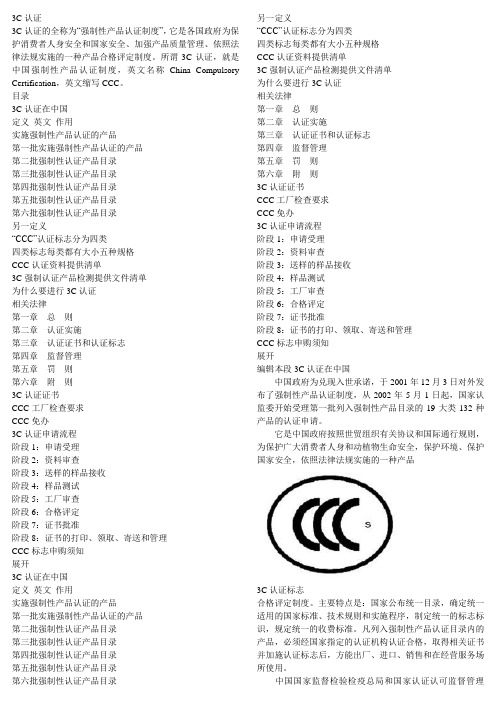
3C认证3C认证的全称为“强制性产品认证制度”,它是各国政府为保护消费者人身安全和国家安全、加强产品质量管理、依照法律法规实施的一种产品合格评定制度。
所谓3C认证,就是中国强制性产品认证制度,英文名称China Compulsory Certification,英文缩写CCC。
目录3C认证在中国定义英文作用实施强制性产品认证的产品第一批实施强制性产品认证的产品第二批强制性认证产品目录第三批强制性认证产品目录第四批强制性认证产品目录第五批强制性认证产品目录第六批强制性认证产品目录另一定义“CCC”认证标志分为四类四类标志每类都有大小五种规格CCC认证资料提供清单3C强制认证产品检测提供文件清单为什么要进行3C认证相关法律第一章总则第二章认证实施第三章认证证书和认证标志第四章监督管理第五章罚则第六章附则3C认证证书CCC工厂检查要求CCC免办3C认证申请流程阶段1:申请受理阶段2:资料审查阶段3:送样的样品接收阶段4:样品测试阶段5:工厂审查阶段6:合格评定阶段7:证书批准阶段8:证书的打印、领取、寄送和管理CCC标志申购须知展开3C认证在中国定义英文作用实施强制性产品认证的产品第一批实施强制性产品认证的产品第二批强制性认证产品目录第三批强制性认证产品目录第四批强制性认证产品目录第五批强制性认证产品目录第六批强制性认证产品目录另一定义“CCC”认证标志分为四类四类标志每类都有大小五种规格CCC认证资料提供清单3C强制认证产品检测提供文件清单为什么要进行3C认证相关法律第一章总则第二章认证实施第三章认证证书和认证标志第四章监督管理第五章罚则第六章附则3C认证证书CCC工厂检查要求CCC免办3C认证申请流程阶段1:申请受理阶段2:资料审查阶段3:送样的样品接收阶段4:样品测试阶段5:工厂审查阶段6:合格评定阶段7:证书批准阶段8:证书的打印、领取、寄送和管理CCC标志申购须知展开编辑本段3C认证在中国中国政府为兑现入世承诺,于2001年12月3日对外发布了强制性产品认证制度,从2002年5月1日起,国家认监委开始受理第一批列入强制性产品目录的19大类132种产品的认证申请。
申请强制性3c认证产品描述

注:如提供的样柜有不同的过电压类别应予以说明。 4)材料组别: Ⅲa 5)污染等级: 3 级 6)电气间隙: ≥10mm 7)爬电距离: ≥14mm 8)无功补偿电容量:360 kvar 9)额定无功电流: 486A 10)电容器组接线方式:电容器部为三角形连接和星形连接 11)控制器:采用基波功率因数和基波无功功率复合控制电容器组的投切,投切稳定无投切震荡。 12)自动投切延时时间:2s~30s 连续可调 13)母线连接处的温长极限:小于或等于 70K 14)隔室空间(柜)的温升极限:30K 15)外壳防护等级:IP30 16)回路数:1 路主回路,16 个分支回路 17)短时耐受电流:15kA 18)触电保护类别:I■、II□、III□ 19)进线保护导体端子和裸露导电部件之间的电阻:不大于 100mΩ 20)装置动态响应时间为:20ms~2000ms 21)符合标准:GB/T15576-2008 22)补偿方式:三相/单相、混合补偿; 23)户外型、户型: 户型
电器股份人民电器厂 ABB 公司
西门子公司 施耐德电气公司
精益电器厂 联容电控
华通开关厂 市德盛电器开关厂
良信电器 正泰电器股份 德力西电气 伊顿-穆勒电气公司 之江开关股份
富士电器 三菱电器 市华中电器 施耐德电气公司 ABB 公司 正泰电器股份 德力西电气 德力西集团 电器瓷厂 正泰电器股份 燎原电器制造有限公 电器股份人民电器厂 施耐德电气公司 ABB 公司 德力西电气 正泰电器股份
本企业对提供所有与认证有关资料的真实性负责。如果本企业获证的产品有 所变更,将及时提交产品变更报告,否则由此引起任何事情本企业将承担全部责 任。
3C认证产品知识简介

只要有下列生产工序,就应制定相应的工艺作业指 导书:拉线、退火、炼胶、挤出、成缆、交联/硫化、 编织。 可行时,工厂应对适宜的过程参数和产品特性进行监 控。工厂应对退火、炼胶、挤出、交联/硫化、编织 的主要工艺参数和产品特性进行监控并保存监控记 录。
第二章 电线电缆3C产品关键工序 及控制要求
主要内容
一、电线电缆3C认证产品范围、执行标准 二、电线电缆3C认证产品关键工序及控制要求 三、电线电缆3C认证产品关键原材料 四、电线电缆3C认证产品确认检验、目击试验、例 行试验项目及试验注意点 五、运行检查 六、检测过程发现的产品质量问题
第一章 电线电缆3C认证产品范围、 执行标准
5、导体电阻 产品标准及GB/3956-1997,导体直流电阻测量值不 大于标准规定的相应值。 问题: ①RVS线导体直流电阻值超过标准规定。 ②60245 IEC 81(YH)电焊机电缆导体直流电阻值超过 标准规定,而其电阻值在产品标准GB/T5013.6-2008 表一有规定,而不是GB/T 3956-1997的第5种导体;
序号 1
产品名称 额定电压450/750V及以下聚氯 乙烯绝缘电线电缆
产品执行标准 GB/T 5023.1~5,7《额定电压450/750V及以 下聚氯乙烯绝缘电缆》、GB/T 5023.6 、 JB/T 8734 《额定电压450/750V及以下聚氯 乙烯绝缘电缆电线和软线》、附件6聚氯乙烯 绝缘软电缆补充要求 、附件7电梯电缆和挠 性连接用电缆补充要求 GB /T5013.1~7《额定电压450/750V及以下橡 皮绝缘电缆》、GB/T 5013.8 、JB/T 8735 《额定电压450/750V及以下橡皮绝缘软线和 软电缆》 GB/T 12972《矿用橡套软电缆》 GB/T 12528.1 《交流额定电压3kV及以下铁 路机车车辆用电缆电线》、GB/T 12528.11 《补充件1:交联聚烯烃绝缘铁路机车车辆用 电缆电线》、JB/T 8145 《交流额定电压3kV 及以下铁路机车车辆用电缆电线》
TDA16833中文资料

P-DSO-14-11 for Applications with Pout ≤ 20 W: TDA 16831G/2G/3G
Pin
Symbol
Function
1
GND
PWM GND and CoolMOS Source
2
FB
PWM Feedback Input
3
N.C.
Not Connected
4
The bias circuit provides the internal circuits with constant current.
Oscillator (osc)
The oscillator is generating a frequency twice the switching frequency
N.C.
Not Connected
5, 6, 7 D
600 V Drain CoolMOS
8, 9, 10 D
600 V Drain CoolMOS
11
N.C.
Not Connected
12
N.C.
Not Connected
13
VCC
14
GND
PWM Supply Voltage PWM GND and Source of CoolMOS
元器件交易网
Off-line SMPS Controller with 600 V Sense CoolMOS on Board
Preliminary Data
Overview
Features
• PWM controller + sense CoolMOS attached in one compact package
EP3C16Q240C8中文资料(Altera)中文数据手册「EasyDatasheet - 矽搜」

1–5
电气特性
直流特性
本节列出I / O漏电流,引脚电容,片上端接(OCT)耐受性,并为Cyclone III器 件总线防护持规范.
电源电流
待机电流是流经器件电流在该装置没有配置输入或输出翻转,在该装置没有活动电流 .使用基于Excel早期功耗估算(EPE)来获取电源电流估计为您设计,因为这些电 流变化在很大程度上与使用资源.
图1-1
示出方法来确定过冲持续时间.
图1-1,
Unit % % % % % % % % % % % % % %
超调
图 1-1. Cyclone III器件超调时间
4.2 V 4.1 V 3.3 V
T T
芯片中文手册,看全文,戳
1–4
第 1章: Cyclone III器件数据表
电气特性
电源电压为输出缓冲器,3.3-V
手术
—
1.15 1.2 1.25
V
—
3.135 3.3 3.465 V
电源电压为输出缓冲器,3.0-V
手术
—
2.85
3
3.15
V
VCCIO (3), (4)
电源电压为输出缓冲器,2.5-V
手术
电源电压为输出缓冲器,1.8-V
手术
电源电压为输出缓冲器,1.5-V
手术
—
2.375 2.5 2.625 V
TSTG TJ
储存温度 工作结温
注意 表 1-1:
(1)电源电压规格适用于电压器件引脚采取相对于地面,而不是在读 电源.
(1)
Min –0.5 –0.5 –0.5 –0.5 –0.5 –25 —
— –65 –40
最大允许过冲或冲电压
- 1、下载文档前请自行甄别文档内容的完整性,平台不提供额外的编辑、内容补充、找答案等附加服务。
- 2、"仅部分预览"的文档,不可在线预览部分如存在完整性等问题,可反馈申请退款(可完整预览的文档不适用该条件!)。
- 3、如文档侵犯您的权益,请联系客服反馈,我们会尽快为您处理(人工客服工作时间:9:00-18:30)。
Key Benefits Modular Fast Ethernet with Feature-rich Layer 3 Switching
3COM ®
SWITCH 4005 DATA SHEET 3Com Corporation, Corporate Headquarters, 5400 Bayfront Plaza, P .O. Box 58145, Santa Clara, CA 95052-8145To learn more about 3Com solutions, visit . 3Com Corporation is publicly traded on Nasdaq under the symbol COMS.
Copyright © 2002 3Com Corporation. All rights reserved. 3Com is a registered trademark of 3Com Corporation. The 3Com logo is a trademark of 3Com Corporation. All other company and product names may be trademarks of their respective companies. While every effort is made to ensure the information given is accurate, 3Com does not accept liability for any errors or mistakes which may arise. All specifications are subject to change without notice.
400670-010 01/033Com Switch 4005 40-Port Copper Fast Ethernet Starter Kit (RJ-45 connectors)3C16830Switch 4005 32-Port Copper and Fiber Fast Ethernet Starter Kit (RJ-45, MT -RJ)3C16831Switch 4005 10-Port Copper Gigabit Ethernet Starter Kit (RJ-45)3C16832Switch 4005 10-Port Fiber Gigabit Ethernet Starter Kit (MT -RJ)3C16833Software Switch 4005 v2.0 Advanced Software 3C16844For units running earlier versions to upgrade
to version 2.0 features Modules Switch 4005 8-port 10/100BASE-TX Module (RJ-45)3C16828Switch 4005 8-port 100BASE-FX Module
(MT -RJ)3C16829Switch 4005 1-Port 1000BASE-SX Module (SC connector)3C16825Switch 4005 1-Port 1000BASE-T Module
(RJ-45)3C16827Modules , continued
Switch 4005 1-Port GBIC Module **(GBIC)3C16826Switch 4005 2-Port 1000BASE-T Module (RJ-45)3C16841Switch 4005 2-Port 1000BASE-SX Module
(MT -RJ)3C16842Switch 4005 2-Port GBIC Module **(GBIC)3C16843Spare Components Switch 4005 Chassis/Power Supply/
Fan/Fabric/Management 3C16820
Switch 4005 300-Watt Power Supply 3C16822Switch 4005 Fan Assembly 3C16823Switch 4005 Fabric/Managment Module 3C16824Spare GBICs
1000BASE-SX GBIC 3CGBIC911000BASE-LX GBIC 3CGBIC921000BASE-LH70 GBIC 3CGBIC97
Ordering Information Dimensions Height: 22.23 cm (8.75 in)Width: 43.94 cm (17.3 in)Depth: 43.68 cm (17.2 in)Weight: 22.68 kg (50 lb)Performance 24 Gbps total bandwidth 18 Mpps forwarding performance RIP v1 and RIP v2OSPF UDP/DHCP Helper DVMRP Multicast Routing Access Control Lists 256 VLANs Link Aggregation (802.3ad trunking)Fast Spanning Tree Protocol 802.1p and 802.1Q 802.3x flow control Power 300 W AC Power Supply Input voltage: 90-264 V AC,autoranging Operating frequency: 47-63 Hz Maximum input current: 6 A at 100 V AC; 3.1 A at 200 V AC Maximum Power Consumption 455 W (1,553 Btu/hour)Environmental Ranges Operating temperature: 0°to 50°C (32°to 122°F)Operating humidity: 10% to 90% noncondensing Storage temperature: -40°to 70°C (-40°to 158°F)Storage humidity: 10% to 90% noncondensing SNMP Standards SNMP Protocol (RFC 1157)MIB-II (RFC1213)Bridge MIB (RFC 1493)RMON MIB II (RFC 2021)Remote Monitoring MIB (RFC 1557)MAU MIB (RFC 2239)Electromagnetic Compatibility The Switch 4005 is certified with the following standards:CE Mark Australian Declaration of Conformity for tick-mark Emissions FCC, Part 15 Subpart B, Class A Canada, ICES003, Class A VCCI Class A EN 55022/CISPR 22, Class A AS/NZS 3548, Class A CNS 13438, Class A Korea No. 34, Class A Safety CSA/NRTL (UL1950, CSA 22.2.950, 3rd Edition)TUV/GS (EN 60950, 3rd Edition,including Amendments and Annexes ZB, ZC; with GS Mark (Bauart Mark for power supplies)CB Report/Certificate to IEC 60950, including all national deviations Management 3Com Network Supervisor (trial copy provided on accompanying CD)Backup and Restore Web Management Command line interface SNMP Four RMON groups Warranty One year hardware warranty;ninety (90) days software warranty. Refer to /warranty for details.Specifications
**GBIC ordered separately.。