MAX1239MEEE+T中文资料
MAX9015AEKA-T中文资料
MAX9016AEKA-T MAX9017AEKA-T MAX9017BEKA-T
Ordering Information continued at end of data sheet. Pin Configurations appear at end of data sheet. Beyond-the-Rails is a trademark of Maxim Integrated Products, Inc. Rail-to-Rail is a registered trademark of Nippon Motorola, Ltd.
元器件交易网
19-2874; Rev 1; 7/03
SOT23, Dual, Precision, 1.8V, Nanopower Comparators With/Without Reference
General Description
The single MAX9015/MAX9016 and dual MAX9017– MAX9020 nanopower comparators in space-saving SOT23 packages feature Beyond-the-Rails™ inputs and are guaranteed to operate down to 1.8V. The Agrade packages feature an on-board 1.236V ±1% reference, while the B-grade packages feature a 1.24V ±1.75% reference. An ultra-low supply current of 0.85µA (MAX9019/MAX9020), 1µA (MAX9015/MAX9016), or 1.2µA (MAX9017/MAX9018) makes the MAX9015– MAX9020 faቤተ መጻሕፍቲ ባይዱily of comparators ideal for all 2-cell battery monitoring/management applications. The unique design of the MAX9015–MAX9020 output stage limits supply-current surges while switching, which virtually eliminates the supply glitches typical of many other comparators. This design also minimizes overall power consumption under dynamic conditions. The MAX9015/MAX9017/MAX9019 have a push-pull output stage that sinks and sources current. Large internal output drivers allow Rail-to-Rail® output swing with loads up to 6mA. The MAX9016/MAX9018/MAX9020 have an open-drain output stage that makes them suitable for mixed-voltage system design. All devices are available in the ultra-small 8-pin SOT23 package. Refer to the MAX9117–MAX9120 data sheet for similar single comparators with or without reference in a tiny SC70 package. o Ultra-Low Total Supply Current 0.85µA (MAX9019/MAX9020) 1.0µA (MAX9015A/MAX9016A) 1.2µA (MAX9017/MAX9018) o Guaranteed Operation Down to 1.8V o Precision VOS < 5mV (max) o Internal 1.236V ±1% Reference (A Grade) o Input Voltage Range Extends 200mV Beyond-the-Rails o CMOS Push-Pull Output with ±6mA Drive Capability (MAX9015/MAX9017/MAX9019) o Open-Drain Output Versions Available (MAX9016/MAX9018/MAX9020) o Crowbar-Current-Free Switching o Internal 4mV Hysteresis for Clean Switching o No Phase Reversal for Overdriven Inputs o Dual Versions in Space-Saving 8-Pin SOT23 Package
MAX202EEWE+T中文资料
________________________________________________________________Maxim Integrated Products 1General DescriptionThe MAX202E–MAX213E, MAX232E/MAX241E line drivers/receivers are designed for RS-232 and V.28communications in harsh environments. Each transmitter output and receiver input is protected against ±15kV electrostatic discharge (ESD) shocks, without latchup.The various combinations of features are outlined in the Selector Guide.The drivers and receivers for all ten devices meet all EIA/TIA-232E and CCITT V.28specifications at data rates up to 120kbps, when loaded in accordance with the EIA/TIA-232E specification.The MAX211E/MAX213E/MAX241E are available in 28-pin SO packages, as well as a 28-pin SSOP that uses 60% less board space. The MAX202E/MAX232E come in 16-pin TSSOP, narrow SO, wide SO, and DIP packages. The MAX203E comes in a 20-pin DIP/SO package, and needs no external charge-pump capacitors. The MAX205E comes in a 24-pin wide DIP package, and also eliminates external charge-pump capacitors. The MAX206E/MAX207E/MAX208E come in 24-pin SO, SSOP, and narrow DIP packages. The MAX232E/MAX241E operate with four 1µF capacitors,while the MAX202E/MAX206E/MAX207E/MAX208E/MAX211E/MAX213E operate with four 0.1µF capacitors,further reducing cost and board space.________________________ApplicationsNotebook, Subnotebook, and Palmtop Computers Battery-Powered Equipment Hand-Held EquipmentNext-Generation Device Featureso For Low-Voltage ApplicationsMAX3222E/MAX3232E/MAX3237E/MAX3241E/MAX3246E: ±15kV ESD-Protected Down to10nA, +3.0V to +5.5V, Up to 1Mbps, True RS-232Transceivers (MAX3246E Available in a UCSP™Package)o For Low-Power ApplicationsMAX3221/MAX3223/MAX3243: 1µA SupplyCurrent, True +3V to +5.5V RS-232 Transceivers with Auto-Shutdown™o For Space-Constrained ApplicationsMAX3233E/MAX3235E: ±15kV ESD-Protected,1µA, 250kbps, +3.0V/+5.5V, Dual RS-232Transceivers with Internal Capacitorso For Low-Voltage or Data Cable ApplicationsMAX3380E/MAX3381E: +2.35V to +5.5V, 1µA,2Tx/2Rx RS-232 Transceivers with ±15kV ESD-Protected I/O and Logic PinsMAX202E–MAX213E, MAX232E/MAX241E±15kV ESD-Protected, +5V RS-232 TransceiversSelector Guide19-0175; Rev 6; 3/05Pin Configurations and Typical Operating Circuits appear at end of data sheet.YesPARTNO. OF RS-232DRIVERSNO. OF RS-232RECEIVERSRECEIVERS ACTIVE IN SHUTDOWNNO. OF EXTERNAL CAPACITORS(µF)LOW-POWER SHUTDOWNTTL TRI-STATE MAX202E 220 4 (0.1)No No MAX203E 220None No No MAX205E 550None Yes Yes MAX206E 430 4 (0.1)Yes Yes MAX207E 530 4 (0.1)No No MAX208E 440 4 (0.1)No No MAX211E 450 4 (0.1)Yes Yes MAX213E 452 4 (0.1)Yes Yes MAX232E 220 4 (1)No No MAX241E454 (1)YesFor pricing, delivery, and ordering information,please contact Maxim/Dallas Direct!at 1-888-629-4642, or visit Maxim’s website at .AutoShutdown and UCSP are trademarks of Maxim Integrated Products, Inc.Ordering InformationOrdering Information continued at end of data sheet.2_______________________________________________________________________________________M A X 202E –M A X 213E , M A X 232E /M A X 241EABSOLUTE MAXIMUM RATINGSV CC ..........................................................................-0.3V to +6V V+................................................................(V CC - 0.3V) to +14V V-............................................................................-14V to +0.3V Input VoltagesT_IN............................................................-0.3V to (V+ + 0.3V)R_IN...................................................................................±30V Output VoltagesT_OUT.................................................(V- - 0.3V) to (V+ + 0.3V)R_OUT......................................................-0.3V to (V CC + 0.3V)Short-Circuit Duration, T_OUT....................................Continuous Continuous Power Dissipation (T A = +70°C)16-Pin Plastic DIP (derate 10.53mW/°C above +70°C)....842mW 16-Pin Narrow SO (derate 8.70mW/°C above +70°C).....696mW 16-Pin Wide SO (derate 9.52mW/°C above +70°C)......762mW 16-Pin TSSOP (derate 9.4mW/°C above +70°C)...........755mW20-Pin Plastic DIP (derate 11.11mW/°C above +70°C)...889mW 20-Pin SO (derate 10.00mW/°C above +70°C).............800mW 24-Pin Narrow Plastic DIP(derate 13.33mW/°C above +70°C) ...............................1.07W 24-Pin Wide Plastic DIP(derate 14.29mW/°C above +70°C)................................1.14W 24-Pin SO (derate 11.76mW/°C above +70°C).............941mW 24-Pin SSOP (derate 8.00mW/°C above +70°C)..........640mW 28-Pin SO (derate 12.50mW/°C above +70°C)....................1W 28-Pin SSOP (derate 9.52mW/°C above +70°C)..........762mW Operating Temperature RangesMAX2_ _EC_ _.....................................................0°C to +70°C MAX2_ _EE_ _...................................................-40°C to +85°C Storage Temperature Range.............................-65°C to +165°C Lead Temperature (soldering, 10s).................................+300°CELECTRICAL CHARACTERISTICS(V CC = +5V ±10% for MAX202E/206E/208E/211E/213E/232E/241E; V CC = +5V ±5% for MAX203E/205E/207E; C1–C4 = 0.1µF for MAX202E/206E/207E/208E/211E/213E; C1–C4 = 1µF for MAX232E/241E; T A = T MIN to T MAX ; unless otherwise noted. Typical values are at T A = +25°C.)Stresses beyond those listed under “Absolute Maximum Ratings” may cause permanent damage to the device. These are stress ratings only, and functional operation of the device at these or any other conditions beyond those indicated in the operational sections of the specifications is not implied. Exposure to absolute maximum rating conditions for extended periods may affect device reliability.ELECTRICAL CHARACTERISTICS (continued)MAX202E–MAX213E, MAX232E/MAX241E (V CC= +5V ±10% for MAX202E/206E/208E/211E/213E/232E/241E; V CC= +5V ±5% for MAX203E/205E/207E; C1–C4 = 0.1µF forMAX202E/206E/207E/208E/211E/213E; C1–C4 = 1µF for MAX232E/241E; T A= T MIN to T MAX; unless otherwise noted. Typical valuesare at T A= +25°C.)Note 1:MAX211EE_ _ tested with V CC= +5V ±5%._______________________________________________________________________________________34______________________________________________________________________________________M A X 202E –M A X 213E , M A X 232E /M A X 241E__________________________________________Typical Operating Characteristics(Typical Operating Circuits, V CC = +5V, T A = +25°C, unless otherwise noted.)5.00MAX211E/MAX213ETRANSMITTER OUTPUT VOLTAGEvs. LOAD CAPACITANCELOAD CAPACITANCE (pF)V O H , -V O L (V )5.56.06.57.07.58.0100020003000400050000MAX211E/MAX213E/MAX241E TRANSMITTER SLEW RATE vs. LOAD CAPACITANCELOAD CAPACITANCE (pF)S L E W R A T E ( V /µs )5101520253010002000300040005000_______________________________________________________________________________________5MAX202E–MAX213E, MAX232E/MAX241E____________________________Typical Operating Characteristics (continued)(Typical Operating Circuits, V CC = +5V, T A = +25°C, unless otherwise noted.)2MAX202E/MAX203E/MAX232E TRANSMITTER SLEW RATE vs. LOAD CAPACITANCELOAD CAPACITANCE (pF)S L E W R A T E ( V /µs )468101214100020003000400050005.07.5-7.53000MAX205E–MAX208ETRANSMITTER OUTPUT VOLTAGEvs. LOAD CAPACITANCE-5.02.5LOAD CAPACITANCE (pF)O U T P U T V O L T A G E (V )10002000400050000-2.54550203000MAX205E–MAX208E SUPPLY CURRENT vs. LOAD CAPACITANCE2540LOAD CAPACITANCE (pF)S U P P L Y C U R R E N T (m A )100020004000500035302.55.0-10.0180MAX205E –MAX208EOUTPUT VOLTAGE vs. DATA RATE-7.50DATA RATE (kbps)O U T P U T V O L T A G E (V )601202401503090210-2.5-5.010.07.56_______________________________________________________________________________________M A X 202E –M A X 213E , M A X 232E /M A X 241EMAX203EMAX205E_____________________________________________________________Pin DescriptionsMAX202E/MAX232E_______________________________________________________________________________________7MAX202E–MAX213E, MAX232E/MAX241EMAX208E________________________________________________Pin Descriptions (continued)MAX206EMAX207E8_______________________________________________________________________________________M A X 202E –M A X 213E , M A X 232E /M A X 241EMAX211E/MAX213E/MAX241E)(MAX205E/MAX206E/MAX211E/MAX213E/MAX241E)________________________________________________Pin Descriptions (continued)MAX211E/MAX213E/MAX241EFigure 3. Transition Slew-Rate Circuit_______________Detailed Description The MAX202E–MAX213E, MAX232E/MAX241E consist of three sections: charge-pump voltage converters, drivers (transmitters), and receivers. These E versions provide extra protection against ESD. They survive ±15kV discharges to the RS-232 inputs and outputs, tested using the Human Body Model. When tested according to IEC1000-4-2, they survive ±8kV contact-discharges and ±15kV air-gap discharges. The rugged E versions are intended for use in harsh environments or applications where the RS-232 connection is frequently changed (such as notebook computers). The standard (non-“E”) MAX202, MAX203, MAX205–MAX208, MAX211, MAX213, MAX232, and MAX241 are recommended for applications where cost is critical.+5V to ±10V Dual Charge-PumpVoltage Converter The +5V to ±10V conversion is performed by dual charge-pump voltage converters (Figure 4). The first charge-pump converter uses capacitor C1 to double the +5V into +10V, storing the +10V on the output filter capacitor, C3. The second uses C2 to invert the +10V into -10V, storing the -10V on the V- output filter capacitor, C4.In shutdown mode, V+ is internally connected to V CC by a 1kΩpull-down resistor, and V- is internally connected to ground by a 1kΩpull up resistor.RS-232 Drivers With V CC= 5V, the typical driver output voltage swing is ±8V when loaded with a nominal 5kΩRS-232 receiver. The output swing is guaranteed to meet EIA/TIA-232E and V.28 specifications that call for ±5V minimum output levels under worst-case conditions. These include a 3kΩload, minimum V CC, and maximum operating temperature. The open-circuit output voltage swings from (V+ - 0.6V) to V-.Input thresholds are CMOS/TTL compatible. The unused drivers’ inputs on the MAX205E–MAX208E, MAX211E, MAX213E, and MAX241E can be left unconnected because 400kΩpull up resistors to V CC are included on-chip. Since all drivers invert, the pull up resistors force the unused drivers’ outputs low. The MAX202E, MAX203E, and MAX232E do not have pull up resistors on the transmitter inputs._______________________________________________________________________________________9MAX202E–MAX213E, MAX232E/MAX241E10______________________________________________________________________________________M A X 202E –M A X 213E , M A X 232E /M A X 241E±15kV ESD-Protected, +5V RS-232 Transceivers When in low-power shutdown mode, the MAX205E/MAX206E/MAX211E/MAX213E/MAX241E driver outputs are turned off and draw only leakage currents—even if they are back-driven with voltages between 0V and 12V. Below -0.5V in shutdown, the transmitter output is diode-clamped to ground with a 1k Ωseries impedance.RS-232 ReceiversThe receivers convert the RS-232 signals to CMOS-logic output levels. The guaranteed 0.8V and 2.4V receiver input thresholds are significantly tighter than the ±3V thresholds required by the EIA/TIA-232E specification.This allows the receiver inputs to respond to TTL/CMOS-logic levels, as well as RS-232 levels.The guaranteed 0.8V input low threshold ensures that receivers shorted to ground have a logic 1 output. The 5k Ωinput resistance to ground ensures that a receiver with its input left open will also have a logic 1 output. Receiver inputs have approximately 0.5V hysteresis.This provides clean output transitions, even with slow rise/fall-time signals with moderate amounts of noise and ringing.In shutdown, the MAX213E’s R4 and R5 receivers have no hysteresis.Shutdown and Enable Control (MAX205E/MAX206E/MAX211E/MAX213E/MAX241E)In shutdown mode, the charge pumps are turned off,V+ is pulled down to V CC , V- is pulled to ground, and the transmitter outputs are disabled. This reduces supply current typically to 1µA (15µA for the MAX213E).The time required to exit shutdown is under 1ms, as shown in Figure 5.ReceiversAll MAX213E receivers, except R4 and R5, are put into a high-impedance state in shutdown mode (see Tables 1a and 1b). The MAX213E’s R4 and R5 receivers still function in shutdown mode. These two awake-in-shutdown receivers can monitor external activity while maintaining minimal power consumption.The enable control is used to put the receiver outputs into a high-impedance state, to allow wire-OR connection of two EIA/TIA-232E ports (or ports of different types) at the UART. It has no effect on the RS-232 drivers or the charge pumps.N ote: The enabl e control pin is active l ow for the MAX211E/MAX241E (EN ), but is active high for the MAX213E (EN). The shutdown control pin is active high for the MAX205E/MAX206E/MAX211E/MAX241E (SHDN), but is active low for the MAX213E (SHDN ).Figure 4. Charge-Pump DiagramMAX202E–MAX213E, MAX232E/MAX241EV+V-200µs/div3V 0V 10V 5V 0V -5V -10VSHDNMAX211EFigure 5. MAX211E V+ and V- when Exiting Shutdown (0.1µF capacitors)X = Don't care.*Active = active with reduced performanceSHDN E N OPERATION STATUS Tx Rx 00Normal Operation All Active All Active 01Normal Operation All Active All High-Z 1XShutdownAll High-ZAll High-ZTable 1a. MAX205E/MAX206E/MAX211E/MAX241E Control Pin ConfigurationsTable 1b. MAX213E Control Pin ConfigurationsThe MAX213E’s receiver propagation delay is typically 0.5µs in normal operation. In shutdown mode,propagation delay increases to 4µs for both rising and falling transitions. The MAX213E’s receiver inputs have approximately 0.5V hysteresis, except in shutdown,when receivers R4 and R5 have no hysteresis.When entering shutdown with receivers active, R4 and R5 are not valid until 80µs after SHDN is driven low.When coming out of shutdown, all receiver outputs are invalid until the charge pumps reach nominal voltage levels (less than 2ms when using 0.1µF capacitors).±15kV ESD ProtectionAs with all Maxim devices, ESD-protection structures are incorporated on all pins to protect against electrostatic discharges encountered during handling and assembly. The driver outputs and receiver inputs have extra protection against static electricity. Maxim’s engineers developed state-of-the-art structures to protect these pins against ESD of ±15kV without damage. The ESD structures withstand high ESD in all states: normal operation, shutdown, and powered down. After an ESD event, Maxim’s E versions keep working without latchup, whereas competing RS-232products can latch and must be powered down to remove latchup.ESD protection can be tested in various ways; the transmitter outputs and receiver inputs of this product family are characterized for protection to the following limits:1)±15kV using the Human Body Model2)±8kV using the contact-discharge method specifiedin IEC1000-4-23)±15kV using IEC1000-4-2’s air-gap method.ESD Test ConditionsESD performance depends on a variety of conditions.Contact Maxim for a reliability report that documents test set-up, test methodology, and test results.Human Body ModelFigure 6a shows the Human Body Model, and Figure 6b shows the current waveform it generates when discharged into a low impedance. This model consists of a 100pF capacitor charged to the ESD voltage of interest, which is then discharged into the test device through a 1.5k Ωresistor.S H D N ENOPERATION STATUS Tx 1–400Shutdown All High-Z 01Shutdown All High-Z 10Normal Operation 11Normal OperationAll ActiveAll Active Active1–34, 5High-Z ActiveHigh-Z High-Z High-Z Active*High-Z RxM A X 202E –M A X 213E , M A X 232E /M A X 241EIEC1000-4-2The IEC1000-4-2 standard covers ESD testing and performance of finished equipment; it does not specifically refer to integrated circuits. The MAX202E/MAX203E–MAX213E, MAX232E/MAX241E help you design equipment that meets level 4 (the highest level) of IEC1000-4-2, without the need for additional ESD-protection components.The major difference between tests done using the Human Body Model and IEC1000-4-2 is higher peak current in IEC1000-4-2, because series resistance is lower in the IEC1000-4-2 model. Hence, the ESD withstand voltage measured to IEC1000-4-2 is generally lower than that measured using the Human Body Model. Figure 7b shows the current waveform for the 8kV IEC1000-4-2 level-four ESD contact-discharge test.The air-gap test involves approaching the device with a charged probe. The contact-discharge method connects the probe to the device before the probe is energized.Machine ModelThe Machine Model for ESD tests all pins using a 200pF storage capacitor and zero discharge resistance. Its objective is to emulate the stress caused by contact that occurs with handling and assembly during manufacturing. Of course, all pins require this protection during manufacturing, not just RS-232 inputs and outputs. Therefore,after PC board assembly,theMachine Model is less relevant to I/O ports.Figure 7a. IEC1000-4-2 ESD Test ModelFigure 7b. IEC1000-4-2 ESD Generator Current WaveformFigure 6a. Human Body ESD Test ModelFigure 6b. Human Body Model Current Waveform__________Applications InformationCapacitor Selection The capacitor type used for C1–C4 is not critical for proper operation. The MAX202E, MAX206–MAX208E, MAX211E, and MAX213E require 0.1µF capacitors, and the MAX232E and MAX241E require 1µF capacitors, although in all cases capacitors up to 10µF can be used without harm. Ceramic, aluminum-electrolytic, or tantalum capacitors are suggested for the 1µF capacitors, and ceramic dielectrics are suggested for the 0.1µF capacitors. When using the minimum recommended capacitor values, make sure the capacitance value does not degrade excessively as the operating temperature varies. If in doubt, use capacitors with a larger (e.g., 2x) nominal value. The capacitors’ effective series resistance (ESR), which usually rises at low temperatures, influences the amount of ripple on V+ and V-.Use larger capacitors (up to 10µF) to reduce the output impedance at V+ and V-. This can be useful when “stealing” power from V+ or from V-. The MAX203E and MAX205E have internal charge-pump capacitors. Bypass V CC to ground with at least 0.1µF. In applications sensitive to power-supply noise generated by the charge pumps, decouple V CC to ground with a capacitor the same size as (or larger than) the charge-pump capacitors (C1–C4).V+ and V- as Power Supplies A small amount of power can be drawn from V+ and V-, although this will reduce both driver output swing and noise margins. Increasing the value of the charge-pump capacitors (up to 10µF) helps maintain performance when power is drawn from V+ or V-.Driving Multiple Receivers Each transmitter is designed to drive a single receiver. Transmitters can be paralleled to drive multiple receivers.Driver Outputs when Exiting Shutdown The driver outputs display no ringing or undesirable transients as they come out of shutdown.High Data Rates These transceivers maintain the RS-232 ±5.0V minimum driver output voltages at data rates of over 120kbps. For data rates above 120kbps, refer to the Transmitter Output Voltage vs. Load Capacitance graphs in the Typical Operating Characteristics. Communication at these high rates is easier if the capacitive loads on the transmitters are small; i.e., short cables are best.Table 2. Summary of EIA/TIA-232E, V.28 SpecificationsMAX202E–MAX213E, MAX232E/MAX241EM A X 202E –M A X 213E , M A X 232E /M A X 241E____________Pin Configurations and Typical Operating Circuits (continued)Table 3. DB9 Cable ConnectionsCommonly Used for EIA/TIAE-232E and V.24 Asynchronous Interfaces____________Pin Configurations and Typical Operating Circuits (continued)MAX202E–MAX213E, MAX232E/MAX241EM A X 202E –M A X 213E , M A X 232E /M A X 241E____________Pin Configurations and Typical Operating Circuits (continued)MAX202E–MAX213E, MAX232E/MAX241E____________Pin Configurations and Typical Operating Circuits (continued)M A X 202E –M A X 213E , M A X 232E /M A X 241E____________Pin Configurations and Typical Operating Circuits (continued)MAX202E–MAX213E, MAX232E/MAX241E____________Pin Configurations and Typical Operating Circuits (continued)M A X 202E –M A X 213E , M A X 232E /M A X 241E____________Pin Configurations and Typical Operating Circuits (continued)______________________________________________________________________________________21MAX202E–MAX213E, MAX232E/MAX241E Ordering Information (continued)*Dice are specified at T A= +25°C.M A X 202E –M A X 213E , M A X 232E /M A X 241E22________________________________________________________________________________________________________________________________________________Chip Topographies___________________Chip InformationC1-V+C1+V CC R2INT2OUT R2OUT0.117"(2.972mm)0.080"(2.032mm)V-C2+ C2-T2IN T1OUT R1INR1OUT T1INGNDR5INV-C2-C2+C1-V+C1+V CC T4OUTR3IN T3OUTT1OUT 0.174"(4.420mm)0.188"(4.775mm)T4IN R5OUT R4OUT T3IN R4IN EN (EN) SHDN (SHDN)R3OUT T2OUT GNDR1IN R1OUT T2IN R2OUTR2IN T1IN ( ) ARE FOR MAX213E ONLYTRANSISTOR COUNT: 123SUBSTRATE CONNECTED TO GNDTRANSISTOR COUNT: 542SUBSTRATE CONNECTED TO GNDMAX202E/MAX232EMAX211E/MAX213E/MAX241EMAX205E/MAX206E/MAX207E/MAX208E TRANSISTOR COUNT: 328SUBSTRATE CONNECTED TO GNDMAX202E–MAX213E, MAX232E/MAX241E Package InformationM A X 202E –M A X 213E , M A X 232E /M A X 241EPackage Information (continued)MAX202E–MAX213E, MAX232E/MAX241E±15kV ESD-Protected, +5V RS-232 TransceiversMaxim cannot assume responsibility for use of any circuitry other than circuitry entirely embodied in a Maxim product. No circuit patent licenses are implied. Maxim reserves the right to change the circuitry and specifications without notice at any time.Maxim Integrated Products, 120 San Gabriel Drive, Sunnyvale, CA 94086 408-737-7600 ____________________25©2005 Maxim Integrated ProductsPrinted USAis a registered trademark of Maxim Integrated Products, Inc.Package Information (continued)(The package drawing(s) in this data sheet may not reflect the most current specifications. For the latest package outline information go to /packages .)。
MAX232中文资料,MAX232CPE,MAX232EPE,MAX232ECPE,规格书,MAXIM代理商,datasheet,PDF
19-4323; Rev 15; 13;5V ޥ٫Ăۂ لRS-232 ഝڑಹ/ेฏಹ
________________________________ ݣะ
MAX220–MAX249࿅઼ഝڑಹ /ेฏಹLjከཛྷEIA/TIA232EჾࣆV.28/V.24ဳेਊහࣜLjᅐದกྐۨ໗ ޥ±12V ٫ᆚوᄮᅋă
ሦဗಹऔ໎Ӽคࠩ٫֠ޥ٫࿅༇Ljሦกᅑᅢದّڱߔࠞޢ ன৹ჾटࠞޢऋဏ ف5μW ჾăMAX225ĂMAX233Ă MAX235 ჾࣆ MAX245/MAX246/MAX247 ԥၖე༶ԩᆐ औLj༚ऌᅋᅢᄩฺ٫ଁғஎࢵᅘوᄮᅋă
1.0 (0.1) 0.1 — — 1.0 (0.1) — 1.0 (0.1) 1.0 (0.1) 1.0 (0.1) 1.0 (0.1)
1.0 1.0 (0.1) 0.1 0.1 1.0 — — — 1.0 1.0
SHDN & ThreeState No Yes Yes Yes Yes No
No No No No No Yes Yes No No No
_____________________________________________________________________ ၭျӹ
Part Number MAX220 MAX222 MAX223 (MAX213) MAX225 MAX230 (MAX200) MAX231 (MAX201)
MAX232 (MAX202) MAX232A MAX233 (MAX203) MAX233A MAX234 (MAX204) MAX235 (MAX205) MAX236 (MAX206) MAX237 (MAX207) MAX238 (MAX208) MAX239 (MAX209)
MAX3232EEAE+T中文资料

Battery-Powered Equipment Cell Phones Cell-Phone Data Cables Notebook, Subnotebook, and Palmtop Computers
Applications
Printers Smart Phones xDSL Modems
MAX3222EEPN -40°C to +85°C 18 Plastic DIP —
MAX3232ECAE 0°C to +70°C 16 SSOP
—
MAX9939中文资料
General DescriptionThe MAX9939 is a general-purpose, differential-input programmable-gain amplifier (PGA) that is ideal for con-ditioning a variety of wide dynamic range signals such as those found in motor current-sense, medical instru-mentation, and sonar data acquisition applications. I t features SPI ™-programmable differential gains from 0.2V/V to 157V/V, input offset-voltage compensation, and an output amplifier that can be configured either as a high-order active filter or to provide a differential output.The PGA is optimized for high-signal bandwidth and its gain can be programmed to be 0.2V/V, 1V/V, 10V/V,20V/V, 30V/V, 40V/V, 60V/V, 80V/V, 119V/V, and 157V/V.Precision resistor matching provides extremely low gain tempco and high CMRR. Although the MAX9939 oper-ates from a single supply V CC between 2.9V to 5.5V, it can process signals both above and below ground due to the use of an input level-shifting amplifier stage.Furthermore, its inputs are protected to ±16V, allowing it to withstand fault conditions and signal overranges.The output amplifier is designed for high bandwidth and low-bias currents, making it ideal for use in multi-ple-feedback active filter topologies that offer much higher Qs and stopband attenuation than Sallen-Key architectures.The MAX9939 draws 3.4mA of quiescent supply current at 5V, and includes a software-programmable shut-down mode that reduces its supply current to only 13µA. The MAX9939 is available in a 10-pin µMAX ®package and operates over the -40°C to +125°C auto-motive temperature range.ApplicationsSensorless Motor Control Medical Signal ConditioningSonar and General Purpose Data Acquisition Differential to Single-Ended Conversion Differential-Input, Differential-Output Signal AmplificationSensor Interface and Signal ProcessingFeatures♦SPI-Programmable Gains: 0.2V/V to 157V/V♦Extremely Low Gain Tempco♦Integrated Amplifier for R/C Programmable Active Filter ♦Input Offset-Voltage Compensation ♦Input Protection to ±16V ♦13µA Software Shutdown Mode♦-40°C to +125°C Operating Temperature Range ♦10-Pin µMAX PackageMAX9939SPI Programmable-Gain Amplifierwith Input Vos Trim and Output Op Amp________________________________________________________________Maxim Integrated Products119-4329; Rev 0; 11/08Ordering InformationFor pricing, delivery, and ordering information, please contact Maxim Direct at 1-888-629-4642,or visit Maxim's website at .+Denotes a lead-free/RoHS-compliant package.Functional Diagram appears at end of data sheet.SPI is a trademark of Motorola, Inc.µMAX is a registered trademark of Maxim Integrated Products, Inc.Pin ConfigurationM A X 9939SPI Programmable-Gain Amplifierwith Input Vos Trim and Output Op Amp 2_______________________________________________________________________________________ABSOLUTE MAXIMUM RATINGSStresses beyond those listed under “Absolute Maximum Ratings” may cause permanent damage to the device. These are stress ratings only, and functional operation of the device at these or any other conditions beyond those indicated in the operational sections of the specifications is not implied. Exposure to absolute maximum rating conditions for extended periods may affect device reliability.V CC to GND..............................................................-0.3V to +6V INB, OUTA, OUTB, SCLK, DIN, CS ............-0.3V to (V CC + 0.3V)INA+, INA- to GND..................................................-16V to +16V Output Short-Circuit Current Duration........................Continuous Continuous Input Current into Any Terminal.....................±20mA Continuous Power Dissipation (T A = +70°C)10-Pin µMAX (derate 5.6mW/°C above +70°C)...........707mWOperating Temperature Range .........................-40°C to +125°C Junction Temperature......................................................+150°C Storage Temperature Range.............................-65°C to +150°C Lead Temperature (soldering, 10s).................................+300°CELECTRICAL CHARACTERISTICSMAX9939SPI Programmable-Gain Amplifierwith Input Vos Trim and Output Op Amp_______________________________________________________________________________________3CC Note 3:For gain of 0.25V/V, the input common-mode range is -1V to V CC - 2V.Note 4:The input current of a CMOS device is too low to be accurately measured on an ATE and is typically on the order of 1pA.Note 5:Parts are functional with f SCLK = 10MHz.ELECTRICAL CHARACTERISTICS (continued)(V CC = 5V, V GND = 0, V INA+= V INA-, Gain = 10V/V, R OUTA = R OUTB = 1k Ωto V CC /2, T A = T MIN to T MAX , unless otherwise noted.Typical values are at T = +25°C.) (Note 1)M A X 9939SPI Programmable-Gain Amplifierwith Input Vos Trim and Output Op Amp 4_______________________________________________________________________________________Figure 1. SPI Interface Timing DiagramTypical Operating Characteristics(V CC = 5V, V GND = 0, V IN+= V IN-= 0, Gain = 10V/V, R OUTA = R OUTB = 1k Ωto V CC /2, T A = +25°C, unless otherwise noted.)PGA GAIN vs. FREQUENCYFREQUENCY (MHz)G A I N (d B )10.110-60-40-200204060-800.01100PGA GAIN vs. FREQUENCYFREQUENCY (MHz)G A I N (d B )10.1-3-2-10123-40.0110AMPLIFIER B GAIN vs. FREQUENCYFREQUENCY (MHz)G A I N (d B )10.110-60-40-200204060-800.01100AMPLIFIER B GAIN vs. FREQUENCYFREQUENCY (MHz)G A I N (d B )10.1-3-2-10123-40.0110COMMON-MODE REJECTION RATIOvs. FREQUENCYFREQUENCY (MHz)C M R R (d B )1010.010.1-70-60-50-40-30-20-100-800.001100GAIN ERROR vs. TEMPERATUREM A X 9939 t o c 06TEMPERATURE (°C)G A I N E R R O R (%)1109580655035205-10-250.050.100.150.20-40125MAX9939SPI Programmable-Gain Amplifierwith Input Vos Trim and Output Op Amp_______________________________________________________________________________________5Typical Operating Characteristics (continued)(V CC = 5V, V GND = 0, V IN+= V IN-= 0, Gain = 10V/V, R OUTA = R OUTB = 1k Ωto V CC /2, T A = +25°C, unless otherwise noted.)INPUT V OS vs. TEMPERATUREM A X 9939 t o c 07TEMPERATURE (°C)O F F S E T (m V )1109580655035205-10-250.51.01.52.02.53.00-401251ms/divINPUT V OS TRIM RESPONSEOUTA 10mV/divGAIN = 1V/VDIFFERENTIAL PSRR vs. FREQUENCYFREQUENCY (kHz)P S R R (d B )1001-80-60-40-20-1000.0110,000100.11000TOTAL HARMONIC DISTORTIONvs. FREQUENCYFREQUENCY (kHz)D I S T O R T I O N (d B )0.110-100-80-60-40-200-1200.011001NOISE VOLTAGE DENSITYFREQUENCY (Hz)N O I S E D E N S I T Y (n V /√H z )10010,000100010010,0001010100,0001000NOISE VOLTAGE DENSITYFREQUENCY (Hz)N O I S E D E N S I T Y (n V /√H z )10010,00010010001010100,0001000M A X 9939SPI Programmable-Gain Amplifierwith Input Vos Trim and Output Op Amp 6_______________________________________________________________________________________1μs/div RECOVERY FROM INPUT OVERLOAD(PGA, GAIN = 1V/V)INA+ - INA-2V/divMAX9939 toc15OUTA1V/div 400ns/divRECOVERY FROM INPUT OVERLOAD(PGA, GAIN = 157V/V)INA+ - INA-2mV/divMAX9939 toc16OUTA1V/div1μs/divRECOVERY FROM INPUT OVERLOAD(OUTPUT AMPLIFIER)IN 2V/divMAX9939 toc17OUTB 2V/div200μs/divGAIN ADJUST RESPONSEINA+ - INA-2mV/divOUTA 1V/divGAIN = 157V/VGAIN = 40V/VGAIN = 10V/V GAIN = 1V/VTypical Operating Characteristics (continued)(V CC = 5V, V GND = 0, V IN+= V IN-= 0, Gain = 10V/V, R OUTA = R OUTB = 1k Ωto V CC /2, T A = +25°C, unless otherwise noted.)2001004003006005007009008001000406020801001201401601% SETTLING TIME vs. GAIN (PGA)GAIN (V/V)S E T T L I N G T I M E (n s )OUTPUT IMPEDANCE vs. FREQUENCYFREQUENCY (MHz)I M P E D A N C E (Ω)10.10.010.11101000.010.00110MAX9939SPI Programmable-Gain Amplifierwith Input Vos Trim and Output Op Amp_______________________________________________________________________________________7Detailed DescriptionThe MAX9939 is a general-purpose PGA with input off-set trim capability. I ts gain and input offset voltage(V OS ) are SPI programmable. The device also includes an uncommitted output operational amplifier that can be used as either a high-order active filter or to provide a differential output. The device can be put into shut-down through SPI.The gain of the amplifier is programmable between 0.2V/V and 157V/V. The input offset is programmable between ±17mV and can be used to regain output dynamic range in high gain settings. An input offset-volt-age measurement mode enables input offset voltage tobe calibrated out in firmware to obtain excellent DC accuracy.The main amplifier accepts a differential input and pro-vides a single-ended output. The relationship between the differential input and singled-ended output is given by the representative equation:V OUTA = V CC /2 + Gain x (V INA+- V INA-) + Gain x V OSArchitectureThe MAX9939 features three internal amplifiers as shown in the Functional Diagram . The first amplifier (amplifier LVL) is configured as a differential amplifier for differential to single-ended conversion with an input offset-voltage trim network. I t has extremely highTypical Operating Characteristics (continued)(V CC = 5V, V GND = 0, V IN+= V IN-= 0, Gain = 10V/V, R OUTA = R OUTB = 1k Ωto V CC /2, T A = +25°C, unless otherwise noted.)200μs/divCOMMON-MODE REJECTION RESPONSEINA+1V/div INA-1V/divOUTA 2V/divSHUTDOWN CURRENT vs. SUPPLY VOLTAGEM A X 9939 t o c 20VOLTAGE (V)S H U T D O W N C U R R E N T (μA )3.64.0162084122.83.24.85.24.4M A X 9939SPI Programmable-Gain Amplifierwith Input Vos Trim and Output Op Amp 8_______________________________________________________________________________________CMRR, gain accuracy, and very low temperature drift due to precise resistor matching. The output of this amplifier is level shifted to V CC /2.This amplifier is followed by a programmable-gain inverting amplifier (amplifier A) with programmable R F and R I resistors whose gain varies between 0.2V/V and 157V/V. The output of this amplifier is biased at V CC /2 and has extremely high gain accuracy and low temperature drift.The MAX9939 has an uncommitted op amp (amplifier B) whose noninverting input is referenced to V CC /2. Its inverting input and output are externally accessible,allowing it to be configured either as an active filter or as a differential output.A robust input ESD protection scheme allows input volt-ages at INA+ and INA- to reach ±16V without damag-ing the MAX9939, thus making the part extremely attractive for use in front-ends that can be exposed to high voltages during fault conditions. I n addition, its input-voltage range extends down to -V CC /2 (e.g., -2.5V when powered from a 5V single supply) allowing the MAX9939 to translate below ground signals to a 0V to 5V output signal. This feature simplifies interfacing ground-referenced signals with unipolar-input ADCs.SPI-Compatible Serial InterfaceThe MAX9939 has a write-only interface, consisting of three inputs: the clock signal (SCLK), data input (DIN),and chip-select input (CS ). The serial interface works with the clock polarity (CPOL) and clock phase (CPHA)both set to 0 (see Figure 1). I nitiating a write to the MAX9939 is accomplished by pulling CS low. Data is clocked in on the rising edge of each clock pulse, and is written LSB first. Each write to the MAX9939 consistsof 8 bits (1 byte). Pull CS high after the 8th bit has been clocked in to latch the data and before sending the next byte of instruction. Note that the internal register is not updated if CS is pulled high before the falling edge of the 8th clock pulse.Register DescriptionThe MAX9939 consists of three registers: a shift register and two internal registers. The shift register accepts data and transfers it to either of the two internal regis-ters. The two internal registers store data that is used to determine the gain, input offset voltage, and operating modes of the amplifier. The two internal registers are the Input V OS Trim register and Gain register. The format of the 8-bit write to these registers is shown in Tables 1and 2. Data is sent to the shift register LSB first.SEL: The SEL bit selects which internal register is writ-ten to. Set SEL to 0 to write bits D5:D1 to the input V OS trim register. Set SEL to 1 to write D4:D1 to the Gain register (D5 is don’t care when SEL = 1).Figure 2. SPI Interface Timing Diagram (CPOL = CPHA = 0)MAX9939SPI Programmable-Gain Amplifierwith Input Vos Trim and Output Op Amp_______________________________________________________________________________________9SHDN:Set SHDN to 0 for normal operation. Set SHDN to 1 to place the device in a low-power 13µA shutdown mode. In shutdown mode, the outputs OUTA and OUTB are high impedance, however, the SPI decode circuitry is still active. Each instruction requires a write to the SHDN bit.MEAS:The MAX9939 provides a means for measuring its own input offset voltage. When MEAS is set to 1, the I NA- input is disconnected from the input signal path and internally shorted to I NA+. This architecture thus allows the input common-mode voltage to be compen-sated at the application-specific input common-mode voltage of interest. The input offset voltage of the PGA is the output offset voltage divided by the programmed gain without any V OS trim (i.e., V3:V0 set to 0):V OS-INHERENT = (V OUTA - V CC /2)/Gain Program V OS to offset V OS-INHERENT . The input V OS also includes the effect of mismatches in the resistor-dividers. Setting MEAS to 0 switches the inputs back to the signals on INA+ and INA-. Each instruction requires a write to the MEAS bit.Programming GainThe PGA’s gain is set by the bits G3:G0 in the Gain reg-ister. Table 3 shows the relationship between the bits G3:G0 and the amplifier’s gain. The slew rate and small-signal bandwidth (SSBW) of the PGA depend on its gain setting as shown in Table 3.Programming Input Offset Voltage (V OS )The input offset voltage is set by the bits V4:V0 in the Input Offset Voltage Trim register. Bit V4 determines the polarity of the offset. Setting V4 to 0 makes the offset positive, while setting V4 to 1 makes the offset negative.Table 4 shows the relationship between V3:V0 and V OS .To determine the effect of V OS at the output of the ampli-fier for gains other than 1, use the following formula:V OUTA = V CC /2 + Gain x (V OS-INHERENT + V OS )where V OS-INHERENT is the inherent input offset voltage of the amplifier, which can be measured by setting MEAS to 1.Applications InformationUse of Output Amplifier as Active FilterThe output amplifier can be configured as a multiple-feedback active filter as shown in Figure 3, which tradi-tionally has better stopband attenuation characteristics than Sallen-Key filters. These filters also possess inher-ently better distortion performance since there are no common-mode induced effects (i.e., the common-mode voltage of the operational amplifier is always fixed at V CC /2 instead of it being signal dependent such as in Sallen-Key filters). Choose external resistors and capacitors to create lowpass, bandpass, or high-pass filters.M A X 9939SPI Programmable-Gain Amplifierwith Input Vos Trim and Output Op Amp 10______________________________________________________________________________________Differential-Input, Differential-Output PGAThe output amplifier can be configured so that the MAX9939 operates as a differential-input, differential-output programmable gain amplifier. As shown in Figure 4, use a 10k Ωresistor between OUTA and INB,and between INB and OUTB. Such a differential-output configuration is ideal for use in low-voltage applications that can benefit from the 2X output voltage dynamic range when compared to single-ended output format.Use of Output Operational Amplifier as TIACMOS inputs on the output op amp makes it ideal for use as an input transimpedance amplifier (TIA) in cer-tain current-output sensor applications. In such a situ-ation, keep in mind that the inverting input operates at fixed voltage of V CC /2. Use a high-value resistor as a feedback gain element, and use a feedback capacitor in parallel with this resistor if necessary to aid amplifi-er stability in the presence of high photodiode or cable capacitance. The output of this TIA can be rout-ed to I NA+ or I NA- for further processing and signal amplification.Power-Supply BypassingBypass V CC to GND with a 0.1µF capacitor in parallel with a 1µF low-ESR capacitor placed as close as possi-ble to the MAX9939.Table 4. Input Offset-Voltage TrimMAX9939SPI Programmable-Gain Amplifierwith Input Vos Trim and Output Op Amp______________________________________________________________________________________11Figure 3. Using the MAX9939 Output Amplifier as an Anti-Aliasing Filter (Corner Frequency = 1.3kHz) to Maximize Nyquist BandwidthM A X 9939SPI Programmable-Gain Amplifierwith Input Vos Trim and Output Op Amp 12______________________________________________________________________________________Figure 4. Using the MAX9939 as a Differential-Input, Differential-Output PGAChip InformationPROCESS: BiCMOSMAX9939SPI Programmable-Gain Amplifierwith Input Vos Trim and Output Op Amp______________________________________________________________________________________13Functional DiagramM A X 9939SPI Programmable-Gain Amplifierwith Input Vos Trim and Output Op Amp Maxim cannot assume responsibility for use of any circuitry other than circuitry entirely embodied in a Maxim product. No circuit patent licenses are implied. Maxim reserves the right to change the circuitry and specifications without notice at any time.14____________________Maxim Integrated Products, 120 San Gabriel Drive, Sunnyvale, CA 94086 408-737-7600©2008 Maxim Integrated Productsis a registered trademark of Maxim Integrated Products, Inc.Package InformationFor the latest package outline information and land patterns, go to /packages .。
法国溯高美低压产品介绍
熔断器开关 Fuserbloc 32 – 1250 A
• Fuserbloc 32 – 1250 A
主要特点:
• 模块化设计,每极1个模块 • 63A 以下导轨固定 • IP2 (熔断器盖和端子盖) • 试验位子为标准配置 ( 400A以下 ) • 1 至 21 极 • 直接操作 • 正面柜外操作 • 侧面操作 (左侧和右侧) • 可设置辅助触点 • 熔断指示 • 背面连接
正常 / 应急控制 器
ATyS 6
ATyS 3
ATyS C20/C30/C40
SWITCHING RANGE GB 10/2005
ATyS 系列电流等级
ATyS 3:
ATyS 3s : 125 – 1800A,3P/4P 10个电流等级 ATyS 3e : 2000 – 3200A,3P/4P 3个电流等级
SWITCHING RANGE GB 10/2005
熔断器开关 Fuserbloc CD 25 – 32 A
Disconnectable Neutral
GB/DIN:
25A 和 32A (熔断器尺寸: 10x38 和 14x51) 3 极和 3极+ 开关或固定中心极
附件:
• 直接和柜外手柄 • 可断开中性极 • 熔断器熔断指示( DIN 尺寸14x51) • U 型辅助触点模块 • 模块化辅助触模块 • 2x2 可设置 U 型辅助触点
SWITCHING RANGE GB 10/2005
熔断器开关
FUSERBLOC 系列 25 – 1250 A
SWITCHING RANGE GB 10/2005
熔断器开关 Fuserbloc CD 25 – 32 A
MAX999EUK-T中文资料
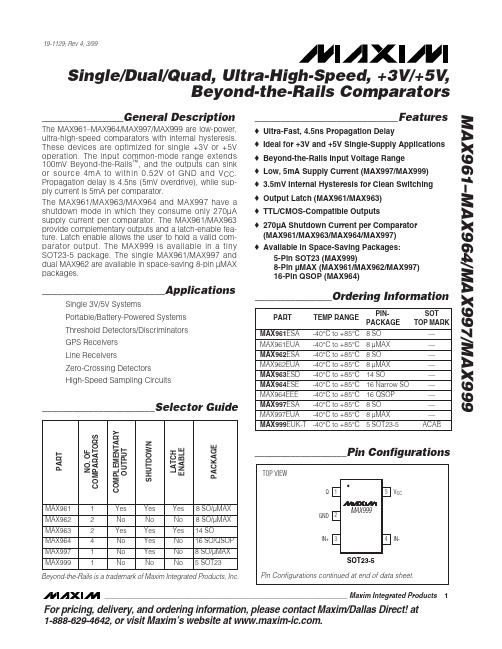
TOP VIEW
Q1 GND 2
MAX999
5 VCC
IN+ 3
4 IN-
SOT23-5 Pin Configurations continued at end of data sheet.
________________________________________________________________ Maxim Integrated Products 1
— — — — — — — — ACAB
PART NO. OF COMPARATORS COMPLEMENTARY OUTPUT SHUTDOWN LATCH ENABLE PACKAGE
__________________Pin Configurations
MAX961
1
MAX962
2
MAX963
PART
TEMP RANGE
PINPACKAGE
SOT TOP MARK
MAX961ESA -40°C to +85°C 8 SO
—
MAX961EUA MAX962ESA MAX962EUA MAX963ESD MAX964ESE MAX964EEE MAX997ESA MAX997EUA MAX999EUK-T
2
MAX964
4
MAX997
1
MAX999
1
Yes Yes Yes 8 SO/µMAX
No
No
No 8 SO/µMAX
Yes Yes Yes 14 SO
No
Yes
No 16 SO/QSOP
No
Yes
No 8 SO/µMAX
No
MAX3313EEUB-T中文资料
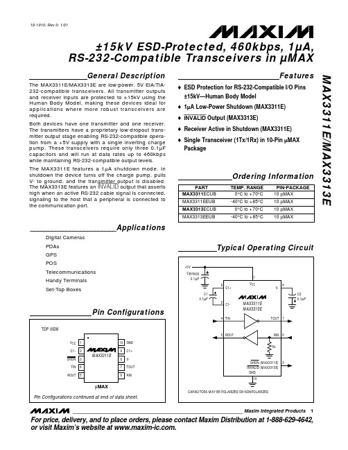
General DescriptionThe MAX3311E/MAX3313E are low-power, 5V EIA/TIA-232-compatible transceivers. All transmitter outputs and receiver inputs are protected to ±15kV using the Human Body Model, making these devices ideal for applications where more robust transceivers are required.Both devices have one transmitter and one receiver.The transmitters have a proprietary low-dropout trans-mitter output stage enabling RS-232-compatible opera-tion from a +5V supply with a single inverting charge pump. These transceivers require only three 0.1µF capacitors and will run at data rates up to 460kbps while maintaining RS-232-compatible output levels.The MAX3311E features a 1µA shutdown mode. In shutdown the device turns off the charge pump, pulls V- to ground, and the transmitter output is disabled.The MAX3313E features an INVALID output that asserts high when an active RS-232 cable signal is connected,signaling to the host that a peripheral is connected to the communication port.________________________ApplicationsDigital Cameras PDAs GPS POSTelecommunications Handy Terminals Set-Top BoxesFeatureso ESD Protection for RS-232-Compatible I/O Pins±15kV—Human Body Modelo 1µA Low-Power Shutdown (MAX3311E)o INVALID Output (MAX3313E)o Receiver Active in Shutdown (MAX3311E)o Single Transceiver (1Tx/1Rx) in 10-Pin µMAX PackageMAX3311E/MAX3313E±15kV ESD-Protected, 460kbps, 1µA,RS-232-Compatible Transceivers in µMAX________________________________________________________________Maxim Integrated Products1Pin Configurations19-1910; Rev 0; 1/01Ordering InformationFor price, delivery, and to place orders,please contact Maxim Distribution at 1-888-629-4642,or visit Maxim’s website at .Typical Operating CircuitM A X 3311E /M A X 3313E±15kV ESD-Protected, 460kbps, 1µA,RS-232-Compatible Transceivers in µMAX 2_______________________________________________________________________________________ABSOLUTE MAXIMUM RATINGSELECTRICAL CHARACTERISTICSStresses beyond those listed under “Absolute Maximum Ratings” may cause permanent damage to the device. These are stress ratings only, and functional operation of the device at these or any other conditions beyond those indicated in the operational sections of the specifications is not implied. Exposure to absolute maximum rating conditions for extended periods may affect device reliability.V CC to GND.............................................................-0.3V to +6V V- to GND................................................................+0.3V to -7V V CC + |V-|............................................................................+13V Input VoltagesTIN, SHDN to GND...............................................-0.3V to +6V RIN to GND......................................................................±25V Output VoltagesTOUT to GND................................................................±13.2V ROUT, INVALID to GND.....................…-0.3V to (V CC + 0.3V)Short-Circuit DurationTOUT to GND.........................................................ContinuousContinuous Power Dissipation10-Pin µMAX (derate 5.6mW/°C above +70°C)..........444mW Operating Temperature RangesMAX331_ECUB.................................................0°C to +70°C MAX331_EEUB..............................................-40°C to +85°C Junction Temperature.....................................................+150°C Storage Temperature Range............................-65°C to +150°C Lead Temperature (soldering, 10s)................................+300°CMAX3311E/MAX3313E±15kV ESD-Protected, 460kbps, 1µA,RS-232-Compatible Transceivers in µMAX_______________________________________________________________________________________3ELECTRICAL CHARACTERISTICS (continued)TIMING CHARACTERISTICSM A X 3311E /M A X 3313E±15kV ESD-Protected, 460kbps, 1µA,RS-232-Compatible Transceivers in µMAX 4_______________________________________________________________________________________Typical Operating Characteristics(V CC = +5V, 0.1µF capacitors, transmitter loaded with 3k Ωand C L , T A = +25°C, unless otherwise noted.)0428612101410001500500200025003000SLEW RATEvs. LOAD CAPACITANCELOAD CAPACITANCE (pF)S L E W R A T E (V /µs )-5-4-3-2-10123456050010001500200025003000TRANSMITTER OUTPUT VOLTAGEvs. LOAD CAPACITANCELOAD CAPACITANCE (pF)T R A N S M I T T E R O U T P U T V O L T A G E (V )010001500500200025003000SUPPLY CURRENT vs. LOAD CAPACITANCELOAD CAPACITANCE (pF)Detailed DescriptionSingle Charge-Pump Voltage ConverterThe MAX3311E/MAX3313E internal power supply has a single inverting charge pump that provides a negative voltage from a single +5V supply. The charge pump operates in a discontinuous mode and requires a flying capacitor (C1) and a reservoir capacitor (C2) to gener-ate the V- supply.RS-232-Compatible DriverThe transmitter is an inverting level translator that con-verts CMOS-logic levels to EIA/TIA-232 compatible lev-els. It guarantees data rates up to 460kbps with worst-case loads of 3k Ωin parallel with 1000pF. When SHDN is driven low, the transmitter is disabled and put into tri-state. The transmitter input does not have an internal pullup resistor.RS-232 ReceiverThe MAX3311E/MAX3313E receiver converts RS-232signals to CMOS-logic output levels. The MAX3311E receiver will remain active during shutdown mode. The MAX3313E INVALID indicates when an RS-232 signal is present at the receiver input, and therefore when the port is in use.The MAX3313E INVALID output is pulled low when no valid RS-232 signal level is detected on the receiver input.MAX3311E Shutdown ModeIn shutdown mode, the charge pump is turned off, V- is pulled to ground, and the transmitter output is disabled (Table 1). This reduces supply current typically to 1µA.The time required to exit shutdown is less than 25ms.Applications InformationCapacitor SelectionThe capacitor type used for C1 and C2 is not critical for proper operation; either polarized or nonpolarized capacitors are acceptable. If polarized capacitors are used, connect polarity as shown in the Typical Operating Circuit . The charge pump requires 0.1µF capacitors. Increasing the capacitor values (e.g., by a factor of 2) reduces power consumption. C2 can beincreased without changing C1’s value. However, do not increase C1’s value without also increasing the value of C2 and C BYPASS to maintain the proper ratios (C1 to the other capacitors).When using the minimum 0.1µF capacitors, make sure the capacitance does not degrade excessively with temperature. If in doubt, use capacitors with a larger nominal value. The capacitor ’s equivalent series resis-tance (ESR) usually rises at low temperatures and influ-ences the amount of ripple on V-.To reduce the output impedance at V-, use larger capacitors (up to 10µF).Bypass V CC to ground with at least 0.1µF. In applica-tions sensitive to power-supply noise generated by the charge pump, decouple V CC to ground with a capaci-tor the same size as (or larger than) charge-pump capacitors C1 and C2.Transmitter Output when ExitingShutdownFigure 1 shows the transmitter output when exiting shutdown mode. The transmitter is loaded with 3k Ωin parallel with 1000pF. The transmitter output displays no ringing or undesirable transients as the MAX3311E comes out of shutdown. Note that the transmitter is enabled only when the magnitude of V- exceeds approximately -3V.High Data RatesThe MAX3311E/MAX3313E maintain RS-232-compati-ble ±3.7V minimum transmitter output voltage even atMAX3311E/MAX3313E±15kV ESD-Protected, 460kbps, 1µA,RS-232-Compatible Transceivers in µMAX5Figure 1. Transmitter Output when Exiting Shutdown or Powering Up10µs/divSHDNTOUT5V/div1.5V/divTIN = GNDTIN = V CCM A X 3311E /M A X 3313E±15kV ESD-Protected, 460kbps, 1µA,RS-232-Compatible Transceivers in µMAX 6_______________________________________________________________________________________high data rates. Figure 2 shows a transmitter loopback test circuit. Figure 3 shows the loopback test result at 120kbps, and Figure 4 shows the same test at 250kbps.±15kV ESD ProtectionAs with all Maxim devices, ESD-protection structures are incorporated on all pins to protect against electro-static discharges encountered during handling and assembly. The MAX3311E/MAX3313E driver outputsand receiver inputs have extra protection against static discharge. Maxim ’s engineers have developed state-of-the-art structures to protect these pins against ESD of ±15kV without damage. The ESD structures withstand high ESD in all states: normal operation, shutdown, and powered down. After an ESD event, Maxim ’s E versions keep working without latchup; whereas, competing products can latch and must be powered down to remove latchup.ESD protection can be tested in various ways. The transmitter outputs and receiver inputs of the product family are characterized for protection to ±15kV using the Human Body Model.ESD Test ConditionsESD performance depends on a variety of conditions.Contact Maxim for a reliability report that documents test setup, test methodology, and test results.Human Body ModelFigure 5 shows the Human Body Model, and Figure 6shows the current waveform it generates when dis-charged into low impedance. This model consists of a 100pF capacitor charged to the ESD voltage of interest,which is then discharged into the test device through a 1.5k Ωresistor.Machine ModelThe Machine Model for ESD tests all pins using a 200pF storage capacitor and zero discharge resis-tance. Its objective is to emulate the stress caused by contact that occurs with handling and assembly during manufacturing. Of course, all pins require this protec-tion during manufacturing, not just RS-232 inputs and outputs. Therefore, after PC board assembly, the Machine Model is less relevant to I/O ports.Figure 4. Loopback Test Results at 250kbps2µs/divTOUTTINROUTFigure 3. Loopback Test Results at 120kbps 5µs/divTOUTTINROUTMAX3311E/MAX3313E±15kV ESD-Protected, 460kbps, 1µA,RS-232-Compatible Transceivers in µMAX_______________________________________________________________________________________7Figure 5. Human Body ESD Test ModelFigure 6. Human Body Current WaveformPin Configurations (continued)Chip InformationTRANSISTOR COUNT: 278M A X 3311E /M A X 3313E±15kV ESD-Protected, 460kbps, 1µA,RS-232-Compatible Transceivers in µMAX Maxim cannot assume responsibility for use of any circuitry other than circuitry entirely embodied in a Maxim product. No circuit patent licenses are implied. Maxim reserves the right to change the circuitry and specifications without notice at any time.8_____________________Maxim Integrated Products, 120 San Gabriel Drive, Sunnyvale, CA 94086 408-737-7600©2001 Maxim Integrated ProductsPrinted USAis a registered trademark of Maxim Integrated Products.______________________________________________________________Pin Description。
- 1、下载文档前请自行甄别文档内容的完整性,平台不提供额外的编辑、内容补充、找答案等附加服务。
- 2、"仅部分预览"的文档,不可在线预览部分如存在完整性等问题,可反馈申请退款(可完整预览的文档不适用该条件!)。
- 3、如文档侵犯您的权益,请联系客服反馈,我们会尽快为您处理(人工客服工作时间:9:00-18:30)。
元器件交易网
2.7V to 3.6V and 4.5V to 5.5V, Low-Power, 4-/12-Channel, 2-Wire Serial, 12-Bit ADCs MAX1236–MAX1239
ABSOLUTE MAXIMUM RATINGS
VDD to GND ..............................................................-0.3V to +6V AIN0–AIN11, REF to GND ............-0.3V to the lower of (VDD + 0.3V) and 6V SDA, SCL to GND.....................................................-0.3V to +6V Maximum Current Into Any Pin .........................................±50mA Continuous Power Dissipation (TA = +70°C) 8-Pin µMAX (derate 4.5mW/°C above +70°C) .............362mW 16-Pin QSOP (derate 8.3mW/°C above +70°C)........666.7mW Operating Temperature Range ...........................-40°C to +85°C Juห้องสมุดไป่ตู้ction Temperature ......................................................+150°C Storage Temperature Range .............................-60°C to +150°C Lead Temperature (soldering, 10s) .................................+300°C
Features
♦ High-Speed I2C-Compatible Serial Interface ♦ ♦ ♦ ♦ ♦ ♦ ♦ ♦ 400kHz Fast Mode 1.7MHz High-Speed Mode Single-Supply 2.7V to 3.6V (MAX1237/MAX1239) 4.5V to 5.5V (MAX1236/MAX1238) Internal Reference 2.048V (MAX1237/MAX1239) 4.096V (MAX1236/MAX1238) External Reference: 1V to VDD Internal Clock 4-Channel Single-Ended or 2-Channel Fully Differential (MAX1236/MAX1237) 12-Channel Single-Ended or 6-Channel Fully Differential (MAX1238/MAX1239) Internal FIFO with Channel-Scan Mode Low Power 670µA at 94.4ksps 230µA at 40ksps 60µA at 10ksps 6µA at 1ksps 0.5µA in Power-Down Mode Software-Configurable Unipolar/Bipolar Small Packages 8-Pin µMAX (MAX1236/MAX1237) 16-Pin QSOP (MAX1238/MAX1239)
元器件交易网
19-2333; Rev 4; 9/06
2.7V to 3.6V and 4.5V to 5.5V, Low-Power, 4-/12-Channel, 2-Wire Serial, 12-Bit ADCs
General Description
The MAX1236–MAX1239 low-power, 12-bit, multichannel analog-to-digital converters (ADCs) feature internal track/hold (T/H), voltage reference, clock, and an I2C-compatible 2-wire serial interface. These devices operate from a single supply of 2.7V to 3.6V (MAX1237/ MAX1239) or 4.5V to 5.5V (MAX1236/MAX1238) and require only 670µA at the maximum sampling rate of 94.4ksps. Supply current falls below 230µA for sampling rates under 46ksps. AutoShutdown™ powers down the devices between conversions, reducing supply current to less than 1µA at low throughput rates. The MAX1236/MAX1237 have four analog input channels each, while the MAX1238/MAX1239 have 12 analog input channels each. The fully differential analog inputs are software configurable for unipolar or bipolar, and single-ended or differential operation. The full-scale analog input range is determined by the internal reference or by an externally applied reference voltage ranging from 1V to V DD . The MAX1237/ MAX1239 feature a 2.048V internal reference and the MAX1236/MAX1238 feature a 4.096V internal reference. The MAX1236/MAX1237 are available in an 8-pin µMAX® package. The MAX1238/MAX1239 are available in a 16pin QSOP package. The MAX1236–MAX1239 are guaranteed over the extended temperature range (-40°C to +85°C). For pin-compatible 10-bit parts, refer to the MAX1136–MAX1139 data sheet. For pin-compatible 8-bit parts, refer to the MAX1036–MAX1039 data sheet.
PART MAX1236EUA MAX1236KEUA MAX1236LEUA MAX1236MEUA MAX1237EUA
Ordering Information
TEMP RANGE -40°C to +85°C -40°C to +85°C -40°C to +85°C -40°C to +85°C -40°C to +85°C -40°C to +85°C -40°C to +85°C -40°C to +85°C -40°C to +85°C -40°C to +85°C -40°C to +85°C -40°C to +85°C PINPACKAGE 8 µMAX 8 µMAX 8 µMAX 8 µMAX 8 µMAX 8 µMAX 8 µMAX 8 µMAX 16 QSOP 16 QSOP 16 QSOP 16 QSOP I2C SLAVE ADDRESS 0110100 0110000 0110010 0110110 0110100 0110000 0110010 0110110 0110101 0110001 0110011 0110111
Selector Guide
PART MAX1236 MAX1237 MAX1238 MAX1239 INTERNAL SUPPLY INPUT REFERENCE VOLTAGE CHANNELS (V) (V) 4 4 12 12 4.096 2.048 4.096 2.048 4.5 to 5.5 2.7 to 3.6 4.5 to 5.5 2.7 to 3.6 INL (LSB) ±1 ±1 ±1 ±1
Stresses beyond those listed under “Absolute Maximum Ratings” may cause permanent damage to the device. These are stress ratings only, and functional operation of the device at these or any other conditions beyond those indicated in the operational sections of the specifications is not implied. Exposure to absolute maximum rating conditions for extended periods may affect device reliability.