DG2301DL-T1-E3中文资料
SI2301CDS-T1-GE3中文资料

Vishay SiliconixSi2301CDSP-Channel 20-V (D-S) MOSFET FEATURES•Halogen-free Option Available•TrenchFET ® Power MOSFETAPPLICATIONS •Load SwitchMOSFET PRODUCT SUMMARYV DS (V)R DS(on) (Ω)I D (A)a Q g (Typ.)- 200.112 at V GS = - 4.5 V - 3.1 3.3 nC0.142 at V GS = - 2.5 V- 2.7Notes:a. Based on T C = 25 °C.b. Surface Mounted on 1" x 1" FR4 board.c. t = 5 s.d. Maximum under Steady State conditions is 175 °C/W.ABSOLUTE MAXIMUM RATINGS T A = 25°C, unless otherwise notedParameter Symbol Limit U nitDrain-Source Voltage V DS - 20VGate-Source Voltage V GS ± 8Continuous Drain Current (T J = 150 °C)T C = 25 °C I D- 3.1A T C = 70 °C - 2.5T A = 25 °C - 2.3b, c T A = 70 °C - 1.8b, cPulsed Drain Current I DM - 10Continuous Source-Drain Diode CurrentT C = 25 °C I S - 1.3T A = 25 °C - 0.72b, c Maximum Power Dissipation T C = 25 °C P D 1.6WT C = 70 °C 1.0T A = 25 °C 0.86b, c T A = 70 °C 0.55b, cOperating Junction and Storage T emperature Range T J , T stg - 55 to 150°C THERMAL RESISTANCE RATINGSParameter Symbol Typical Maximum UnitMaximum Junction-to-Ambient b, d ≤ 5 s R thJA 120145°C/WMaximum Junction-to-Foot (Drain)Steady State R thJF 6278Vishay SiliconixSi2301CDSNotes:a. Pulse test; pulse width ≤ 300 µs, duty cycle ≤ 2 %.b. Guaranteed by design, not subject to production testing.Stresses beyond those listed under “Absolute Maximum Ratings” may cause permanent damage to the device. These are stress ratings only, and functional operation of the device at these or any other conditions beyond those indicated in the operational sections of the specifications is not implied. Exposure to absolute maximum rating conditions for extended periods may affect device reliability.MOSFET SPECIFICATIONS T J = 25°C, unless otherwise notedParameter Symbol Test Conditions Min.Typ.Max.U nit StaticDrain-Source Breakdown Voltage V DS V DS = 0 V, I D = - 250 µA- 20VV DS Temperature Coefficient ΔV DS /T J I D = - 250 µA - 18mV/°C V GS(th) T emperature Coefficient ΔV GS(th)/T J 2.2Gate-Source Threshold Voltage V GS(th) V DS = V GS , I D = - 250 µA - 0.4- 1V Gate-Source LeakageI GSS V DS = 0 V , V GS = ± 8 V ± 100nA Zero Gate Voltage Drain Current I DSS V DS = - 20 V , V GS = 0 V - 1µA V DS = - 20 V, V GS = 0 V , T J = 55 °C- 10On-State Drain Current aI D(on) V DS ≤ - 5 V , V GS = - 4.5 V - 6A Drain-Source On-State Resistance aR DS(on) V GS = - 4.5 V, I D = - 2.8 A 0.0900.112ΩV GS = - 2.5 V, I D = - 2.0 A 0.1100.142Forward T ransconductance a g fsV DS = - 5 V , I D = - 2.8 A2.0SDynamic bInput Capacitance C iss V DS = - 10 V , V GS = 0 V , f = 1 MHz405pFOutput CapacitanceC oss 75Reverse Transfer Capacitance C rss 55Total Gate Charge Q g V DS = - 10 V , V GS = - 4.5 V , ID = - 3 A 5.510nC V DS = - 10 V , V GS = - 2.5 V , I D = - 3 A 3.36Gate-Source Charge Q gs 0.7Gate-Drain Charge Q gd 1.3Gate Resistance R g f = 1 MHz6.0ΩTurn-On Delay Time t d(on) V DD = - 10 V, R L = 10 ΩI D = - 1 A, V GEN = - 4.5 V , R G = 1 Ω1120ns Rise Timet r 3560Turn-Off Delay Time t d(off) 3050Fall Timet f1020Drain-Source Body Diode Characteristics Continuous Source-Drain Diode Current I S T C = 25 °C- 1.3A Pulse Diode Forward Current a I SM - 10Body Diode VoltageV SD I S = - 0.7 A- 0.8- 1.2V Body Diode Reverse Recovery Time t rr I F = - 3.0 A, dI/dt = 100 A/µs, T J = 25 °C3050ns Body Diode Reverse Recovery Charge Q rr 2550nC Reverse Recovery Fall Time t a 15nsReverse Recovery Rise Timet b15Output CharacteristicsOn-Resistance vs. Drain Current and Gate VoltageTransfer CharacteristicsCapacitanceOn-Resistance vs. Junction TemperatureThreshold VoltageSingle Pulse PowerVishay SiliconixSi2301CDSTYPICAL CHARACTERISTICS 25°C, unless otherwise notedVishay Siliconix maintains worldwide manufacturing capability. Products may be manufactured at one of several qualified locations. Reliability data for Silicon Technology and Package Reliability represent a composite of all qualified locations. For related documents such as package/tape drawings, part marking, and reliability data, see /ppg?68741.Normalized Thermal Transient Impedance, Junction-to-FootDisclaimer Legal Disclaimer NoticeVishayAll product specifications and data are subject to change without notice.Vishay Intertechnology, Inc., its affiliates, agents, and employees, and all persons acting on its or their behalf (collectively, “Vishay”), disclaim any and all liability for any errors, inaccuracies or incompleteness contained herein or in any other disclosure relating to any product.Vishay disclaims any and all liability arising out of the use or application of any product described herein or of any information provided herein to the maximum extent permitted by law. The product specifications do not expand or otherwise modify Vishay’s terms and conditions of purchase, including but not limited to the warranty expressed therein, which apply to these products.No license, express or implied, by estoppel or otherwise, to any intellectual property rights is granted by this document or by any conduct of Vishay.The products shown herein are not designed for use in medical, life-saving, or life-sustaining applications unless otherwise expressly indicated. Customers using or selling Vishay products not expressly indicated for use in such applications do so entirely at their own risk and agree to fully indemnify Vishay for any damages arising or resulting from such use or sale. Please contact authorized Vishay personnel to obtain written terms and conditions regarding products designed for such applications.Product names and markings noted herein may be trademarks of their respective owners.元器件交易网。
si2301中文资料

场效应管:场效应晶体管简称场效应管。
主要有两种类型:结型场效应管和金属- 氧化物半导体场效应管。
由多数载流子参与导电,也称为单极型晶体管。
它属于电压控制型半导体器件。
具有输入电阻高、噪声小、功耗低、动态范围大、易于集成、没有二次击穿现象、安全工作区域宽等优点,现已成为双极型晶体管和功率晶体管的强大竞争者。
场效应管是利用控制输入回路的电场效应来控制输出回路电流的一种半导体器件,并以此命名。
由于它仅靠半导体中的多数载流子导电,又称单极型晶体管。
FET 英文为Field Effect Transistor,简写成FET。
简介:SI2301是MOS管的一种,属于场效应管。
主要参数:晶体管类型:P沟道MOSFET最大功耗PD :1.25W栅极门限电压VGS :2.5V(典型值)漏源电压VDS :-20V(极限值)漏极电流ID:TA=25°时:-2.3A,TA=70°时:-1.5A通态电阻RDS(on):0.145ohm(典型值)栅极漏电流IGSS:±100nA结温:55℃to+150℃封装:SOT-23(TO-236)替代型号:WT-2301 WTC2301 SMG2301 CES2301 KI2301BDS封装类型:SOT-23P沟MOS晶体管:金属氧化物半导体场效应(MOS)晶体管可分为N沟道与P沟道两大类,P沟道硅MOS场效应晶体管在N型硅衬底上有两个P+区,分别叫做源极和漏极,两极之间不通导,栅极上加有足够的正电压(源极接地)时,栅极下的N型硅表面呈现P型反型层,成为连接源极和漏极的沟道。
改变栅压可以改变沟道中的电子密度,从而改变沟道的电阻。
这种MOS场效应晶体管称为P沟道增强型场效应晶体管。
如果N型硅衬底表面不加栅压就已存在P型反型层沟道,加上适当的偏压,可使沟道的电阻增大或减小。
这样的MOS场效应晶体管称为P沟道耗尽型场效应晶体管。
统称为PMOS晶体管。
P沟道MOS晶体管的空穴迁移率低,因而在MOS晶体管的几何尺寸和工作电压绝对值相等的情况下,PMOS晶体管的跨导小于N 沟道MOS晶体管。
SI1555DL-T1-E3中文资料

FEATURESD TrenchFET rPower MOSFETPb-free AvailableSi1555DLVishay SiliconixDocument Number: 71079S-50245—Rev. D, 21-Feb-051Complementary Low-Threshold MOSFET PairPRODUCT SUMMARYV DS (V)r DS(on) (W )I D (A)0.385 @ V GS = 4.5 V 0.70N-Channel200.630 @ V GS = 2.5 V 0.540.600 @ V GS = −4.5 V −0.60P-Channel −80.850 @ V GS = −2.5 V −0.501.200 @ V GS = −1.8 V−0.42Marking CodeRBXXLot Traceability and Date CodePart # Code Y YOrdering Information:Si1555DL-T1Si1555DL-T1—E3 (Lead (Pb)-Free)SOT-363SC-70 (6-LEADS)Top ViewS 1G 1D 2D 1G 2S 2ABSOLUTE MAXIMUM RATINGS (T A = 25_C UNLESS OTHERWISE NOTED)N-ChannelP-Channel ParameterSymbol5 secs Steady State5 secsSteady StateUnitDrain-Source Voltage V DS 20−8Gate-Source VoltageV GS "12"8VT A = 25_C "0.70"0.66−0.60−0.57Continuous Drain Current (T J = 150_C)a T A = 85_CI D "0.50"0.48−0.43−0.41Pulsed Drain CurrentI DM "1.0AContinuous Source Current (Diode Conduction)a I S 0.250.23−0.25−0.23Maximum Power Dissipation T A = 25_C 0.300.270.300.27aT A = 85_C P D 0.160.140.160.14W Operating Junction and Storage Temperature RangeT J , T stg−55 to 150_CTHERMAL RESISTANCE RATINGSParameterSymbol TypicalMaximumUnitM iJ ti t A bi t t v 5 sec 360415Maximum Junction-to-Ambient a Steady State R thJA 400460_Maximum Junction-to-Foot (Drain)Steady StateR thJF300350C/WNotesa.Surface Mounted on 1” x 1” FR4 Board.Si1555DLVishay Siliconix2Document Number: 71079S-50245—Rev. D, 21-Feb-05SPECIFICATIONS (T J = 25_C UNLESS OTHERWISE NOTED)ParameterSymbol Test Condition Min Typ Max UnitStaticV DS = V GS , I D = 250 m A N-Ch 0.6 1.4Gate Threshold VoltageV GS(th)V DS = V GS , I D = −250 m A P-Ch −0.45−1.0VGate Body Leakage V DS = 0 V, V GS = "12 V N-Ch "100Gate-Body LeakageI GSSV DS = 0 V, V GS = "8 V P-Ch "100nAV DS = 20 V, V GS = 0 VN-Ch 1V DS = −8 V, V GS = 0 V P-Ch −1Zero Gate Voltage Drain CurrentI DSSV DS = 20 V, V GS = 0 V, T J = 85_C N-Ch 5m A V DS = −8 V, V GS = 0 V, T J = 85_CP-Ch −5On State Drain Current D()V DS w 5 V, V GS = 4.5 V N-Ch 1.0On-State Drain Current aI D(on)V DS p −5 V, V GS = −4.5 V P-Ch −1.0A V GS = 4.5 V, I D = 0.66 A N-Ch 0.3200.385V GS = −4.5 V, I D = −0.57 AP-Ch 0.5100.600Drain-Source On-State Resistance ar V GS = 2.5 V, I D = 0.40 A N-Ch 0.5600.630WDS(on)V GS = −2.5 V, I D = −0.48 A P-Ch 0.7200.850V GS = −1.8 V, I D = −0.20 AP-Ch 1.00 1.200Forward Transconductance f V DS = 10 V, I D = 0.66 A N-Ch 1.5ag fs V DS = −4 V, I D = −0.57 A P-Ch 1.2S Diode Forward Voltage I S = 0.23 A, V GS = 0 V N-Ch 0.8 1.2a V SDI S = −0.23 A, V GS = 0 VP-Ch−0.8−1.2VDynamic bN-Ch 0.8 1.2Total Gate ChargeQ gN-ChannelP-Ch 1.5 2.3Gate Source Charge V DS = 10 V, V GS = 4.5 V, I D = 0.66 A N-Ch 0.06Gate-Source ChargeQ gs P-Channel4 V 45 V I 057 AP-Ch 0.17nCGate Drain Charge d V DS = −4 V, V GS = −4.5 V, I D = −0.57 A N-Ch 0.30Gate-Drain ChargeQ gd P-Ch 0.16Turn On Delay Time d()N-Ch 1020Turn-On Delay Timet d(on)P-Ch612N-ChannelN-Ch 1630Rise Timet r V DD = 10 V, R L = 20 WI D ^ 0.5 A, V GEN = 4.5 V, R = 6 W P-Ch 2550Turn Off Delay Time d(ff)g P-Channel V 4 V R 8 WN-Ch 1020Turn-Off Delay Timet d(off)DD = −4 V, R L = 8 I −0.5 A, V −4.5 V, R P-Ch 1020nsD ^ GEN = g = 6 WN-Ch 1020Fall Timet f P-Ch1020Source-DrainI F = 0.23 A, di/dt = 100 A/m s N-Ch 2040Reverse Recovery Timet rrI F = −0.23 A, di/dt = 100 A/m sP-Ch2040Notesa.Pulse test; pulse width v 300 m s, duty cycle v 2%.b.Guaranteed by design, not subject to production testing.Stresses beyond those listed under “Absolute Maximum Ratings” may cause permanent damage to the device. These are stress ratings only, and functional operation of the device at these or any other conditions beyond those indicated in the operational sections of the specifications is not implied. Exposure to absolute maximum rating conditions for extended periods may affect device reliability.Si1555DLVishay SiliconixDocument Number: 71079S-50245—Rev. D, 21-Feb-0530.00.5 1.0 1.5 2.0 2.50.00.51.01.52.02.53.0V DS − Drain-to-Source Voltage (V)V GS − Gate-to-Source Voltage (V)2040608010048121620− O n -R e s i s t a n c e (r D S (o n )W )0.60.81.01.21.41.6−50−2502550751001251500123450.00.20.40.60.80.00.20.40.60.81.00.00.20.40.60.81.0V DS − Drain-to-Source Voltage (V)On-Resistance vs. Drain Current− G a t e -t o -S o u r c e V o l t a g e (V )Q g − Total Gate Charge (nC)C − C a p a c i t a n c e (p F )V G S CapacitanceOn-Resistance vs. Junction TemperatureT J − Junction Temperature (_C)r D S (o n ) − O n -R e s i i s t a n c e (N o r m a l i z e d )Si1555DLVishay Siliconix4Document Number: 71079S-50245—Rev. D, 21-Feb-05TYPICAL CHARACTERISTICS (25_C UNLESS NOTED)N−CHANNEL0.00.20.40.60.81.01.20.00.20.40.60.81.01234510.1− O n -R e s i s t a n c e (r D S (o n )W )V SD − Source-to-Drain Voltage (V)V GS − Gate-to-Source Voltage (V)− S o u r c e C u r r e n t (A )I S 03512P o w e r (W )Single Pulse PowerTime (sec)411006001010−110−210−3−0.4−0.3−0.2−0.1−0.00.10.2−50−250255075100125150210.10.01Threshold VoltageV a r i a n c e (V )V G S (t h )T J − Temperature (_C)Normalized Thermal Transient Impedance, Junction-to-AmbientSquare Wave Pulse Duration (sec)N o r m a l i z e d E f f e c t i v e T r a n s i e n t T h e r m a l I m p e d a n c eSi1555DLVishay SiliconixDocument Number: 71079S-50245—Rev. D, 21-Feb-055TYPICAL CHARACTERISTICS (25_C UNLESS NOTED)N−CHANNEL10−310−211010−110−4210.10.01Normalized Thermal Transient Impedance, Junction-to-FootSquare Wave Pulse Duration (sec)N o r m a l i z e d E f f e c t i v e T r a n s i e n t T h e r m a l I m p e d a n c e0.00.5 1.0 1.5 2.0 2.5V GS − Gate-to-Source Voltage (V)40801201602468− O n -R e s i s t a n c e (r D S (o n )W )0.00.51.01.52.00.00.20.40.60.81.0V DS − Drain-to-Source Voltage (V)I D − Drain Current (A)C − C a p a c i t a n c e (p F )CapacitanceSi1555DLVishay Siliconix6Document Number: 71079S-50245—Rev. D, 21-Feb-050.00.20.40.60.8 1.0 1.2 1.4 1.6Q g − Total Gate Charge (nC)0.00.20.40.60.81.01.20.00.51.01.52.01234510.1− O n -R e s i s t a n c e (r D S (o n )W )V SD − Source-to-Drain Voltage (V)V GS − Gate-to-Source Voltage (V)− S o u r c e C u r r e n t (A )I S 03512P o w e r (W )Single Pulse PowerTime (sec)411006001010−110−210−3−0.2−0.10.00.10.20.30.4−50−250255075100125150Threshold VoltageV a r i a n c e (V )V G S (t h )T J − Temperature (_C)Si1555DLVishay SiliconixDocument Number: 71079S-50245—Rev. D, 21-Feb-057TYPICAL CHARACTERISTICS (25_C UNLESS NOTED)P−CHANNEL210.10.01Normalized Thermal Transient Impedance, Junction-to-AmbientSquare Wave Pulse Duration (sec)N o r m a l i z e d E f f e c t i v e T r a n s i e n t T h e r m a l I m p e d a n c e10−310−211010−110−4210.10.01Normalized Thermal Transient Impedance, Junction-to-FootSquare Wave Pulse Duration (sec)N o r m a l i z e d E f f e c t i v e T r a n s i e n t T h e r m a l I m p e d a n c eVishay Siliconix maintains worldwide manufacturing capability. Products may be manufactured at one of several qualified locations. Reliability data for Silicon T echnology and Package Reliability represent a composite of all qualified locations. For related documents such as package/tape drawings, part marking, and reliability data, see /ppg?71079.Document Number: 91000Revision: 18-Jul-081DisclaimerLegal Disclaimer NoticeVishayAll product specifications and data are subject to change without notice.Vishay Intertechnology, Inc., its affiliates, agents, and employees, and all persons acting on its or their behalf (collectively, “Vishay”), disclaim any and all liability for any errors, inaccuracies or incompleteness contained herein or in any other disclosure relating to any product.Vishay disclaims any and all liability arising out of the use or application of any product described herein or of any information provided herein to the maximum extent permitted by law. The product specifications do not expand or otherwise modify Vishay’s terms and conditions of purchase, including but not limited to the warranty expressed therein, which apply to these products.No license, express or implied, by estoppel or otherwise, to any intellectual property rights is granted by this document or by any conduct of Vishay.The products shown herein are not designed for use in medical, life-saving, or life-sustaining applications unless otherwise expressly indicated. Customers using or selling Vishay products not expressly indicated for use in such applications do so entirely at their own risk and agree to fully indemnify Vishay for any damages arising or resulting from such use or sale. Please contact authorized Vishay personnel to obtain written terms and conditions regarding products designed for such applications.Product names and markings noted herein may be trademarks of their respective owners.元器件交易网。
SI2301-TP;中文规格书,Datasheet资料
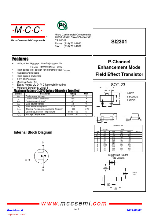
SI2301P-ChannelEnhancement Mode Field Effect TransistorFeatures• -20V,-2.8A, R DS(ON)=120m Ω@V GS =-4.5V R DS(ON)=150m Ω@V GS =-2.5V• High dense cell design for extremely low R DS(ON) • Rugged and reliable • High Speed Switching Micro Commercial Componentsomp onents 20736 Marilla Street Chatsworth! "# $ % ! "#Electrical CharacteristicsT A =25C unless otherwise notedParameterSymbol Min Units Off CharacteristicsDrain-Source Breakdown Voltage Zero Gate Voltage Drain Current Gate Body Leakage Current,Forward Forward Transconductance Gate Threshold Voltage Static Drain-Source On-ResistanceBV DSS I DSS I GSSR I GSSF 12080-0.45-100100-1m ΩV nA nA µAVS Gate Body Leakage Current,Reverse On Characteristics c Dynamic Characteristics d Input Capacitance Reverse Transfer Capacitance Output CapacitanceSwitching Characteristics d Turn-On Delay Time Turn-Off Fall Time Turn-Off Delay Time Turn-On Rise Time Total Gate Charge Gate-Source Charge Gate-Drain ChargeDrain-Source Diode Characteristics and Maximun RatingsDrain-Source Diode Forward Current b Drain-Source Diode Forward VoltagecTest Condition V GS =0V,I D =-250µA V GS(th)R DS(on)g FS C iss C oss C rss t d(on)t r t d(off)t f Q g Q gs Q gd I S V SDTypMax-20V DS =-20V,V GS =0V V GS =8V,V DS =0V V GS =-8V,V DS =0V V GS =V DS ,I D =-250µA V GS =-4.5V,I D =-2.8A V GS =-2.5V,I D =-2.0A V DS =-5V,I D =-2.8AV DD =-6V,I D =-1A,V GS =-4.5V,R GEN =6ΩV DS =-6V,I D =-2.8A,V GS =-4.5V V DS =-6V,V GS =0V,f =1.0MHzV GS =0V,I S =-0.75A 880270175115322320106545111.52.114.5-0.75-1.28150110m ΩpF pF pF ns ns ns ns nC nC nC A VNotes :a.Repetitive Rating :Pulse width limited by maximum junction temperature.b.Surface Mounted on FR4Board,t <5sec.c.Pulse Test :Pulse Width <300µs,Duty Cycle <2%.d.Guaranteed by design,not subject to production testing.SI 2301Micro Commercial ComponentsC ,C a p a c i t a n c e (p F )-I D ,D r a i n C u r r e n t (A )C issC oss C rss1200100080060040020000246810-I D ,D r a i n C u r r e n t (A )R D S (O N ),N o r m a l i z e d R D S (O N ),O n -R e s i s t a n c e (O h m s )-V DS ,Drain-to-Source Voltage (V)Figure 1.Output Characteristics-V GS ,Gate-to-Source Voltage (V)Figure 2.Transfer Characteristics-V DS ,Drain-to-Source Voltage (V)Figure 3.CapacitanceT J ,Junction Temperature(C)Figure 4.On-Resistance Variationwith Temperature2.21.91.61.31.00.70.4-100-50050100150200V T H ,N o r m a l i z e d G a t e -S o u r c e T h r e s h o l d V o l t a g eT J ,JunctionTemperature(C)Figure 5.Gate Threshold Variationwith Temperature1.31.21.11.00.90.80.70.6-50-25255075100125150-I S ,S o u r c e -d r a i n c u r r e n t (A )-V SD ,Body Diode Forward Voltage (V)Figure 6.Body Diode Forward VoltageVariation with Source Current1086420014532108642101010.20.40.60.810-11.21.0SI 2301Micro Commercial ComponentsMicro Commercial ComponentsOrdering Information :Device PackingPart Number-TP Tape&Reel: 3Kpcs/Reel***IMPORTANT NOTICE***Micro Commercial Components Corp. reserve s the right to make changes without further notice to any product herein to make corrections, modifications , enhancements , improvements , or other changes . Micro Commercial Components Corp . does not assume any liability arising out of the application or use of any product described herein; neither does it convey any license under its patent rights ,nor the rights of others . The user of products in such applications shall assume all risks of such use and will agree to hold Micro Commercial Components Corp . and all the companies whose products are represented on our website, harmless against all damages.***LIFE SUPPORT***MCC's products are not authorized for use as critical components in life support devices or systems without the express writtenapproval of Micro Commercial Components Corporation.***CUSTOMER AWARENESS***Counterfeiting of semiconductor parts is a growing problem in the industry. Micro Commercial Components (MCC) is taking strong measures to protect ourselves and our customers from the proliferation of counterfeit parts. MCC strongly encourages customers to purchase MCC parts either directly from MCC or from Authorized MCC Distributors who are listed by country on our web page cited below. Products customers buy either from MCC directly or from Authorized MCC Distributors are genuine parts, have full traceability, meet MCC's quality standards for handling and storage. MCC will not provide any warranty coverage or other assistance for parts bought from Unauthorized Sources. MCC is committed to combat this global problem and encourage our customers to do their part in stopping this practice by buying direct or from authorized distributors./分销商库存信息: MICRO-COMMERICAL-CO SI2301-TP。
KD-2301工业自动化说明书(S7200)解读
KD-2301工业自动化综合实训装置实训指导书本手册适用于KD-2301工业自动化综合实训装置,包括了使用时的操作说明和实验内容。
不正确的使用可能发生意想不到的事故,使用实验设备进行实验之前,请仔细阅读可编程控制器操作手册和其他相关元件的使用手册。
请将此手册送呈最终用户。
前言概述可编程控制器,Programmable Logic Controller,简称PLC,是现代工业自动化领域的三大支柱(PLC、机器人、CAD/CAM)之一,因其卓越的性能而得到广泛的应用.PLC从1968年出现到现在,随着高性能微处理器的飞速发展,PLC的性能已经由单一的逻辑控制功能发展为具有过程控制功能、运动控制功能、数据处理功能、联网通信功能的真正名副其实的多功能控制器.PLC的高可靠性,使它成为了现代控制CIMS系统中不可或缺的基本组成部分,人们高度评价PLC的重要性.PLC配合变频调速器、伺服控制器、各类传感器、智能模块等设备,广泛的应用于各种工业控制现场,如楼宇自动化、电梯、恒压供水系统、流水生产线等.在PLC众多的优越性能当中,最卓越的性能是其网络通信功能,随着计算机技术的飞速发展,人们要求自动化系统具有开放性、集散性、智能性、信息电子化与网络化等特点,并且能用工控机对系统实现方便快捷的控制,显然单机自动化系统已经远远不能满足工业控制要求,在这一形势下,包括三菱、欧姆龙、西门子、松下、莫迪康等著名的PLC生产厂家陆续推出了各种类型的PLC网络,PLC网络的应用也越来越普遍和广泛.因此,掌握PLC及其网络系统的应用技术成了各类电气自动化工作人员重要任务,PLC及其网络的应用技术也已经成为了各类自动化专业学生的核心课程.我公司利用西门子公司的各种PLC产品,开发了这套专门用于教学过程的PLC实验系统.丰富的基础实验内容,使学生更深入的掌握PLC单机的硬件和软件的应用.系统具备强大的扩展性能,组态监控软件、传感器以及PLC网络的加入,让学生可轻松的掌握西门子的组网方法和编制一般的通信应用程序,以及学会怎样利用组态软件制作各种人机界面对PLC的 I/O点进行远程监视和控制.系统采用西门子可编程控制器300为主机,将I/O点的接口全部引到主机模块的面板上,用插接导线配合单元模块就能方便的完成各种实验.学生可通过手持编程器(输入语句表)或个人电脑(输入语句表、梯形图)进行程序的编制、调试和运行.通过辅助模块,还可以用PLC直接带动电机负载,进行电机的各种启动、运行演示,使学生可以全面的掌握可编程控制器的控制原理、安装操作、指令训练、编程技巧等。
SI5504BDC-T1-E3;中文规格书,Datasheet资料
N- and P-Channel 30 V (D-S) MOSFETPRODUCT SUMMARYV DS (V)R DS(on) (Ω)I D (A)Q g (Typ)N-Channel 300.065 at V GS = 10 V 4a 2 nC 0.100 at V GS = 4.5 V 4a P-Channel- 300.140 at V GS = - 10 V - 3.7 2.2 nC0.235 at V GS = - 4.5 V- 2.8Notes:a.Package limited.b.Surface mounted on 1" x 1" FR4 board.c.t = 5 s.d.See Reliability Manual for profile. The ChipFET is a leadless package. The end of the lead terminal is exposed copper (not plated) as a result of the singulation process in manufacturing. A solder fillet at the exposed copper tip cannot be guaranteed and is not required to ensure adequade bottom side solder interconnection.e.Rework conditions: manual soldering with a soldering iron is not recommended for leadless components.f.Maximum under steady state conditions is 120 °C/W.ABSOLUTE MAXIMUM RATINGS T A = 25°C, unless otherwise notedParameter Symbol N-Channel P-Channel UnitDrain-Source VoltageV DS 30- 30VGate-Source VoltageV GS ± 20Continuous Drain Current (T J = 150 °C)T C = 25 °C I D 4a - 3.7A T C = 85 °C 3.8- 2.7T A = 25 °C 3.7b, c - 2.5b, c T A = 85 °C 2.6b, c- 1.8b, c Pulsed Drain Current I DM 10- 10Source Drain Current Diode CurrentT C = 25 °C I S 2.5- 2.5T A = 25 °C 1.3b, c - 1.3b, c Maximum Power Dissipation T C = 25 °C P D 3.12 3.1W T C = 85 °C 22T A = 25 °C 1.5b, c 1.5b, c T A = 85 °C 0.8b, c0.8b, c Operating Junction and Storage Temperature Range T J , T stg - 55 to 150°C Soldering Recommendations (Peak Temperature)d, e260THERMAL RESISTANCE RATINGSParameter Symbol N-ChannelP-ChannelUnitTyp.Max.Typ.Max.Maximum Junction-to-Ambient b, f t ≤ 5 s R thJA 70857085°C/WMaximum Junction-to-Foot (Drain)Steady State R thJF 33403340FEATURES•Halogen-free According to IEC 61249-2-21Definition•TrenchFET ® Power MOSFETs•Compliant to RoHS Directive 2002/95/ECAPPLICATIONS•DC/DC for Portable ApplicationsNotes:a. Guaranteed by design, not subject to production testing.b. Pulse test; pulse width ≤ 300 µs, duty cycle ≤ 2 %.SPECIFICATIONS T J = 25°C, unless otherwise notedParameter Symbol Test Conditions Min.Typ.Max.UnitStaticDrain-Source Breakdown Voltage V DS V GS = 0 V , I D = 250 µA N-Ch 30V V GS = 0 V, I D = - 250 µAP-Ch - 30V DS Temperature Coefficient ΔV DS /T J I D = 250 µA N-Ch 27mV/°CI D = - 250 µA P-Ch - 30V GS(th) Temperature Coefficient ΔV GS(th)/T J I D = 250 µA N-Ch - 5I D = - 250 µA P-Ch 3.5Gate Threshold Voltage V GS(th) V DS = V GS , I D = 250 µA N-Ch 1.53VV DS = V GS , I D = - 250 µA P-Ch - 1.5- 3Gate-Body LeakageI GSSV DS = 0 V , V GS = ± 20 V N-Ch 100nAP-Ch - 100Zero Gate Voltage Drain CurrentI DSSV DS = 30 V, V GS = 0 VN-Ch 1µAV DS = - 30 V , V GS = 0 V P-Ch - 1V DS = 30 V , V GS = 0 V, T J = 85 °C N-Ch 5V DS = - 30 V, V GS = 0 V , T J = 85 °CP-Ch - 5On-State Drain CurrentbI D(on)V DS ≥ 5 V , V GS = 10 V N-Ch 10A V DS ≤ - 5 V , V GS = - 10 V P-Ch - 10Drain-Source On-State Resistance b R DS(on)V GS = 10 V , I D = 3.1 A N-Ch 0.0530.065ΩV GS = - 10 V , I D = - 2.1 A P-Ch 0.1120.140V GS = 4.5 V, I D = 1 A N-Ch 0.0810.100V GS = - 4.5 V , I D = - 0.43 A P-Ch 0.1880.235Forward T ransconductance b g fsV DS = 15 V , I D = 3.1 A N-Ch 5S V DS = - 15 V , I D = - 2.1 AP-Ch 3.5Dynamic aInput Capacitance C iss N-ChannelV DS = 15 V, V GS = 0 V , f = 1 MHz P-ChannelV DS = - 15 V , V GS = 0 V , f = 1 MHz N-Ch220pFP-Ch 170Output CapacitanceC oss N-Ch 50P-Ch 50Reverse Transfer CapacitanceC rssN-Ch 25P-Ch 31Total Gate Charge Q gV DS = 15 V, V GS = 10 V, I D = 3.6 AN-Ch 4.57nC V DS = - 15 V , V GS = - 10 V , I D = - 2.5 A P-Ch 4.57N-ChannelV DS = 15 V , V GS = 4.5 V , I D = 3.6 AP-ChannelV DS = - 15 V , V GS = - 4.5 V , I D = - 2.5 AN-Ch 23P-Ch 2.2 3.5Gate-Source Charge Q gs N-Ch 0.7P-Ch 0.7Gate-Drain Charge Q gd N-Ch 0.7P-Ch 1Gate ResistanceR gf = 1 MHzN-Ch 3ΩP-Ch13Notes:a. Guaranteed by design, not subject to production testing.b. Pulse test; pulse width ≤ 300 µs, duty cycle ≤ 2 %.Stresses beyond those listed under “Absolute Maximum Ratings” may cause permanent damage to the device. These are stress ratings only, and functional operation of the device at these or any other conditions beyond those indicated in the operational sections of the specifications is not implied. Exposure to absolute maximum rating conditions for extended periods may affect device reliability.SPECIFICATIONS T J = 25°C, unless otherwise notedParameter Symbol Test Conditions Min.Typ.Max.UnitDynamic aT urn-On Delay Time t d(on) N-ChannelV DD = 15 V, R L = 5.8 Ω I D ≅ 2.6 A, V GEN = 4.5 V , R g = 1 ΩP-ChannelV DD = - 15 V , R L = 7.5 Ω I D ≅ - 2 A, V GEN = - 4.5 V , R g = 1 ΩN-Ch1525nsP-Ch 3045Rise Timet r N-Ch 80120P-Ch 6090T urn-Off Delay Time t d(off) N-Ch 1220P-Ch 1015Fall Timet f N-Ch 2540P-Ch 1015T urn-On Delay Time t d(on) N-ChannelV DD = 15 V, R L = 5.8 Ω I D ≅ 2.6 A, V GEN = 10 V , R g = 1 ΩP-ChannelV DD = - 15 V , R L = 7.5 Ω I D ≅ - 2 A, V GEN = - 10 V , R g = 1 ΩN-Ch48P-Ch 48Rise Timet r N-Ch 1220P-Ch 1015T urn-Off Delay Time t d(off) N-Ch 1015P-Ch 1015Fall Timet fN-Ch 510P-Ch510Drain-Source Body Diode Characteristics Continuous Source-Drain Diode Current I S T C = 25 °CN-Ch 2.5AP-Ch - 2.5Pulse Diode Forward Current a I SM N-Ch 10P-Ch - 10Body Diode VoltageV SD I S = 2.6 A, V GS = 0 V N-Ch 0.8 1.2V I S = - 2 A, V GS = 0 VP-Ch - 0.8- 1.2Body Diode Reverse Recovery Time t rr N-ChannelI F = 2.6 A, dI/dt = 100 A/µs, T J = 25 °C P-ChannelI F = - 2 A, dI/dt = - 100 A/µs, T J = 25 °CN-Ch 3050ns P-Ch 2040Body Diode Reverse Recovery Charge Q rr N-Ch 2040nC P-Ch 1020Reverse Recovery Fall Time t a N-Ch 23nsP-Ch 13Reverse Recovery Rise Timet bN-Ch 7P-Ch7N-CHANNEL TYPICAL CHARACTERISTICS 25°C, unless otherwise notedOutput CharacteristicsOn-Resistance vs. Drain CurrentTransfer CharacteristicsCapacitanceN-CHANNEL TYPICAL CHARACTERISTICS 25°C, unless otherwise notedSource-Drain Diode Forward VoltageThreshold VoltageSingle Pulse PowerSafe Operating Area, Junction-to-AmbientN-CHANNEL TYPICAL CHARACTERISTICS 25°C, unless otherwise noted* The power dissipation P D is based on T J(max) = 150 °C, using junction-to-case thermal resistance, and is more useful in settling the upper dissipation limit for cases where additional heatsinking is used. It is used to determine the current rating, when this rating falls below the package limit.Current Derating*Power DeratingN-CHANNEL TYPICAL CHARACTERISTICS 25°C, unless otherwise notedTransfer CharacteristicsCapacitanceOn-Resistance vs. Junction TemperatureP-CHANNEL TYPICAL CHARACTERISTICS 25°C, unless otherwise notedSource-Drain Diode Forward VoltageSingle Pulse PowerP-CHANNEL TYPICAL CHARACTERISTICS 25°C, unless otherwise noted* The power dissipation P D is based on T J(max) = 150 °C, using junction-to-case thermal resistance, and is more useful in settling the upper dissipation limit for cases where additional heatsinking is used. It is used to determine the current rating, when this rating falls below the package limit.Current Derating*分销商库存信息: VISHAYSI5504BDC-T1-E3。
DG2301中文资料

V+OETop View A B GNDDevice Marking: E4DG2301Vishay SiliconixNew ProductDocument Number: 72049High-Speed, Low r ON , SPST Analog Switch(1-Bit Bus Switch)FEATURESD SC-70 5-Lead PackageD 5-W Switch Connection Between Two PortsD Minimal Propagation Delay Through The Switch D Low I CCD Zero Bounce In Flow-Through ModeDControl Inputs Compatible with TTL LevelDESCRIPTIONThe DG2301 is a high-speed, 1-bit, low power,TTL-compatible bus switch. Using sub-micron CMOS technology, DG2301 achieves low on-resistance and negligible propagation delay.The DG2301 consist of a bi-directional input/output pins A andB. When the output enable (OE) is low, the input/output pins are connected. When the OE is high, the switch is open and a high-impedance state exists between input/output pins A and B.FUNCTIONAL BLOCK DIAGRAM AND PIN CONFIGURATIONTRUTH TABLEOEBFunctionL A Connect HHiZ StateDisconnectORDERING INFORMATIONTemp RangePackagePart Number-40 to 85°CSC70-5DG2301DLDG2301Vishay SiliconixNew ProductDocument Number: 72049ABSOLUTE MAXIMUM RATINGSReference to GNDV+-0.3 to +6 V . . . . . . . . . . . . . . . . . . . . . . . . . . . . . . . . . . . . . . . . . . . . . . . . . . . . OE, A, B a -0.3 to (V+ + 0.3 V). . . . . . . . . . . . . . . . . . . . . . . . . . . . . . . . . . . . . . . . . . . . . . . . Continuous Current (Any terminal) "50 mA . . . . . . . . . . . . . . . . . . . . . . . . . . . Peak Current "200 mA . . . . . . . . . . . . . . . . . . . . . . . . . . . . . . . . . . . . . . . . . . . . . (Pulsed at 1 ms, 10% duty cycle)Storage Temperature (D Suffix)-65 to 150°C. . . . . . . . . . . . . . . . . . . . . . . . . . . . Power Dissipation (Packages)b6-Pin SC70c 250 mW . . . . . . . . . . . . . . . . . . . . . . . . . . . . . . . . . . . . . . . . . . . . . . . Notes:a.Signals on A, or B or OE exceeding V+ will be clamped by internaldiodes. Limit forward diode current to maximum current ratings.b.All leads welded or soldered to PC Board.c.Derate 3.1 mW/_C above 70_CSPECIFICATIONS (V+ = 5.0 V)Test ConditionsOtherwise Unless SpecifiedLimits-40 to 85_CParameterSymbolV+ = 4.0 V to 5.5 V, V OE = 0.8 or 2.0 V eTemp aMin b Typ c Max bUnitDC CharacteristicsV+ = 4.5 V, V A = 0 V, I B = 64 mAFull 7On Resistance V+ = 4.5 V, V A = 0 V, I B = 30 mA Full 7On-Resistancer ONV+ = 4.5 V, V A = 2.4 V, I B = 15 mA Full 15WV+ = 4.0 V, V A = 2.4 V, I B = 15 mAFull 20Switch Off Leakage Current I (off)V+ = 5.5 V, V A = 1 V/4.5 V, V B = 4.5 V/1 VFull -1010Switchl-On Leakage Current I (on)V+ = 5.5 V, V A = V B = 1 V/4.5 VFull -1010m A Input High Voltage V IHFull 2.0Input Low Voltage V IL Full0.8V Input CurrentI IL or I IHV OE = 0 or V+Full-11m ADynamic CharacteristicsProp Delay Bus to Bus t PHL Full 1Prop Delay Bus-to-Bus ft PLH V LD = Open (Figure 1 and 2)Full 1V LD = 7 V, V+ = 4.5 V to 5.5 V (Figure 1 and 2)Full 3.9Output Enable Time t PZLV LD = 7 V, V+ = 4.0 V (Figure 1 and 2)Full 4.5dV LD = Open, V+ = 4.5 V to 5.5 V (Figure 1 and 2)Full 3.7t PZHV LD = Open, V+ = 4.0 V (Figure 1 and 2)Full 4.5nsV LD = 7 V, V+ = 4.5 V to 5.5 V (Figure 1 and 2)Full 4.0Output Disable Time t PLZV LD = 7 V, V+ = 4.0 V (Figure 1 and 2)Full 4.2dV LD = Open, V+ = 4.5 V to 5.5 V (Figure 1 and 2)Full 1.0t PHZV LD = Open, V+ = 4.0 V (Figure 1 and 2)Full 1.0Input Capacitance C inRoom 3.5Channel-Off Capacitance d C (off) = 0 or V+ f = 1 MHzRoom5pF Channel-On Capacitance dC ONV OE = 0 or V+, f = 1 MHz Room11p Power SupplyPower Supply Range V+ 4.05.5V Power Supply Current I+V OE = 0 or V+0.011.0m ANotes:a.Room = 25°C, Full = as determined by the operating suffix.b.The algebraic convention whereby the most negative value is a minimum and the most positive a maximum, is used in this data sheet.c.Typical values are for design aid only, not guaranteed nor subject to production testing.d.Guarantee by design, nor subjected to production test.e.V IN = input voltage to perform proper function.f.Guaranteed by design and not production tested. The bus switch propagation delay is a function of the RC time constant contributed by the on-resistance and the specified load capacitance with an ideal voltage source (zero output impedance) driving the switch.DG2301Vishay SiliconixNew ProductDocument Number: 72049AC LOADING AND WAVEFORMSt rV LD 20 VV LDFigure 2.AC WaveformsDG2301Vishay SiliconixNew ProductDocument Number: 72049TYPICAL CHARACTERISTICS (25_C UNLESS NOTED)02040608010012012345r ON vs. V B Single Supply VoltageV B - Analog Voltage (V)r O N - O n -R e s i s t a n c e (W )This datasheet has been download from: Datasheets for electronics components.。
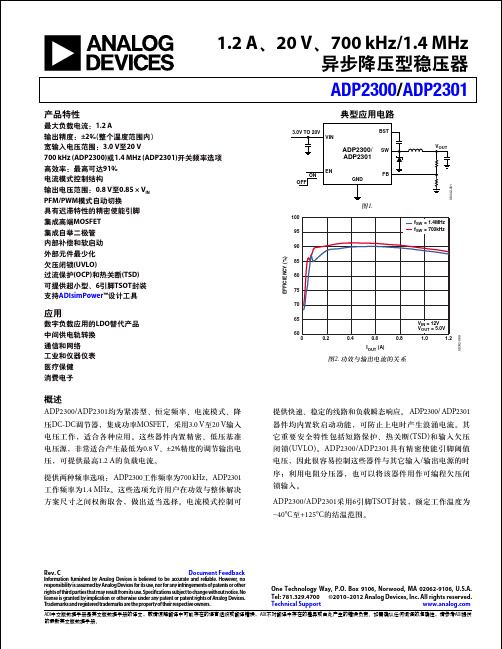
ADP2300_2301_cn开关电源中文版
65 60
0 0.2 0.4 0.6 IOUT (A) 0.8
VIN = 12V VOUT = 5.0V 1.0 1.2
08342-069
图2. 功效与输出电流的关系
概述
ADP2300/ADP2301均为紧凑型、恒定频率、电流模式、降 压DC-DC调节器,集成功率MOSFET,采用3.0 V至20 V输入 电压工作,适合各种应用。这些器件内置精密、低压基准 电压源,非常适合产生最低为0.8 V、±2%精度的调节输出电 压,可提供最高1.2 A的负载电流。 提供两种频率选项: ADP2300工作频率为700 kHz,ADP2301 工作频率为1.4 MHz。这些选项允许用户在功效与整体解决 方案尺寸之间权衡取舍,做出适当选择。电流模式控制可 提供快速、稳定的线路和负载瞬态响应。 ADP2300/ ADP2301 器件均内置软启动功能,可防止上电时产生浪涌电流。其 它重要安全特性包括短路保护、热关断 (TSD)和输入欠压 闭锁 (UVLO)。 ADP2300/ADP2301具有精密使能引脚阈值 电压,因此很容易控制这些器件与其它输入/输出电源的时 序;利用电阻分压器,也可以将该器件用作可编程欠压闭 锁输入。 ADP2300/ADP2301采用6引脚TSOT封装,额定工作温度为 −40°C至+125°C的结温范围。
ADI中文版数据手册是英文版数据手册的译文,敬请谅解翻译中可能存在的语言组织或翻译错误,ADI不对翻译中存在的差异或由此产生的错误负责。如需确认任何词语的准确性,请参考ADI提供 的最新英文版数据手册。
ADP2300/ADP2301
目录
特性 ..............................................................................
- 1、下载文档前请自行甄别文档内容的完整性,平台不提供额外的编辑、内容补充、找答案等附加服务。
- 2、"仅部分预览"的文档,不可在线预览部分如存在完整性等问题,可反馈申请退款(可完整预览的文档不适用该条件!)。
- 3、如文档侵犯您的权益,请联系客服反馈,我们会尽快为您处理(人工客服工作时间:9:00-18:30)。
Vishay SiliconixDG2301High-Speed, Low r ON , SPST Analog Switch(1-Bit Bus Switch)FEATURES•SC-70 5-Lead Package•5Ω Switch Connection Between Two Ports •Minimal Propagation DelayThrough The Switch •Low I CC•Zero Bounce In Flow-Through Mode•Control Inputs Compatible with TTL LevelDESCRIPTIONThe DG2301 is a high-speed, 1-bit, low power, TTL -compatible bus switch. Using sub-micron CMOS technology,DG2301 achieves low on-resistance and negligible propagation delay.The DG2301 consist of a bi-directional input/output pins A pins are connected. When the OE is high, the switch is open and a high-impedance state exists between input/output pins A and B.FUNCTIONAL BLOCK DIAGRAM AND PIN CONFIGURATION* Pb containing terminations are not RoHS compliant, exemptions may applyTRUTH TABLEOE B Function LA Connect HHiZ StateDisconnectORDERING INFORMATIONTemp Range Package Part Number - 40 to 85 °CSC70-5DG2301DL-T1DG2301DL-T1-E3Vishay SiliconixDG2301Notes:a. Signals on A, or B or OE exceeding V+ will be clamped by internal diodes. Limit forward diode current to maximum current ratings.b. All leads welded or soldered to PC Board.c. Derate 3.1 mW/°C above 70 °C.Notes:a. Room = 25 °C, Full = as determined by the operating suffix.b. The algebraic convention whereby the most negative value is a minimum and the most positive a maximum, is used in this data sheet.c. Typical values are for design aid only, not guaranteed nor subject to production testing.d. Guarantee by design, nor subjected to production test.e. V IN = input voltage to perform proper function.f. Guaranteed by design and not production tested. The bus switch propagation delay is a function of the RC time constant contributed by the on-resistance and the specified load capacitance with an ideal voltage source (zero output impedance) driving the switch.Stresses beyond those listed under “Absolute Maximum Ratings” may cause permanent damage to the device. These are stress ratings only, and functional operation of the device at these or any other conditions beyond those indicated in the operational sections of the specifications is not implied. Exposure to absolute maximum rating conditions for extended periods may affect device reliability.ABSOLUTE MAXIMUM RATINGSParameterLimit Unit Reference V+ to GND- 0.3 to + 6V OE, A, B a- 0.3 to (V+ + 0.3)Continuous Current (Any Terminal)± 50mA Peak Current (Pulsed at 1 ms, 10 % duty cycle)± 200Storage T emperature (D Suffix)- 65 to 150°C Power Dissipation (Packages)b6-Pin SC70c250mWSPECIFICATIONS (V+ = 5.0 V)P r ameter Symbol Test ConditionsOtherwise Unless Specified V+ = 4.0 V to 5.5 V , V OE = 0.8 or 2.0 V e Temp aLimits - 40 to 85 °CUnitMin bTyp cMax bDC CharacteristicsOn-Resistancer ON V+ = 4.5 V , V A = 0 V , I B = 64 mA Full 7 ΩV+ = 4.5 V , V A = 0 V , I B = 30 mA Full 7V+ = 4.5 V, V A = 2.4 V, I B = 15 mA Full 15V+ = 4.0 V, V A = 2.4 V, I B = 15 mA Full 20Switch Off Leakage Current I (off)V+ = 5.5 V, V A = 1 V/4.5 V , V B = 4.5 V/1 VFull - 1010µA Switch-On Leakage Current I (on)V+ = 5.5 V, V A = V B = 1 V/4.5 VFull - 1010Input High Voltage V IH Full 2.0V Input Low Voltage V IL Full 0.8Input CurrentI IL or I IH V OE = 0 or V+Full - 11µADynamic Characteristics Prop Delay Bus-to-Bus ft PHL V LD = Open (Figure 1 and 2)Full 1nst PLH Full 1Output Enable Time dt PZLV LD = 7 V , V+ = 4.5 V to 5.5 V (Figure 1 and 2)Full 3.9V LD = 7 V , V+ = 4.0 V (Figure 1 and 2)Full 4.5t PZH V LD = Open, V+ = 4.5 V to 5.5 V (Figure 1 and 2)Full 3.7V LD = Open, V+ = 4.0 V (Figure 1 and 2)Full 4.5Output Disable Time dt PLZV LD = 7 V , V+ = 4.5 V to 5.5 V (Figure 1 and 2)Full 4.0V LD = 7 V , V+ = 4.0 V (Figure 1 and 2)Full 4.2t PHZV LD = Open, V+ = 4.5 V to 5. V (Figure 1 and 2)Full 1.0V LD = Open, V+ = 4.0 V (Figure 1 and 2)Full 1.0Input CapacitanceC in Room 4pF Channel-Off Capacitance dC (off)V OE = 0 or V+, f = 1 MHzRoom 5Channel-On Capacitance d C ONRoom11Power SupplyPower Supply Range V+ 4.0 5.5VPower Supply Current I+V OE = 0 or V+0.01 1.0µAVishay SiliconixDG2301AC LOADING AND WAVEFORMSFigure 1. AC Test CircuitFigure 2. AC WaveformsVishay SiliconixDG2301TYPICAL CHARACTERISTICS 25°C, unless otherwise notedVishay Siliconix maintains worldwide manufacturing capability. Products may be manufactured at one of several qualified locations. Reliability data for Silicon Tech-nology and Package Reliability represent a composite of all qualified locations. For related documents such as package/tape drawings, part marking, and reliability data, see /ppg?72049.r ON vs. V B Single Supply VoltageDisclaimer Legal Disclaimer NoticeVishayAll product specifications and data are subject to change without notice.Vishay Intertechnology, Inc., its affiliates, agents, and employees, and all persons acting on its or their behalf (collectively, “Vishay”), disclaim any and all liability for any errors, inaccuracies or incompleteness contained herein or in any other disclosure relating to any product.Vishay disclaims any and all liability arising out of the use or application of any product described herein or of any information provided herein to the maximum extent permitted by law. The product specifications do not expand or otherwise modify Vishay’s terms and conditions of purchase, including but not limited to the warranty expressed therein, which apply to these products.No license, express or implied, by estoppel or otherwise, to any intellectual property rights is granted by this document or by any conduct of Vishay.The products shown herein are not designed for use in medical, life-saving, or life-sustaining applications unless otherwise expressly indicated. Customers using or selling Vishay products not expressly indicated for use in such applications do so entirely at their own risk and agree to fully indemnify Vishay for any damages arising or resulting from such use or sale. Please contact authorized Vishay personnel to obtain written terms and conditions regarding products designed for such applications.Product names and markings noted herein may be trademarks of their respective owners.元器件交易网。