MAX6306UK43D4中文资料
MAX6303中文资料

( ) ARE FOR MAX6302/MAX6304.
* Patents pending
________________________________________________________________ Maxim Integrated Products 1
For free samples & the latest literature: , or phone 1-800-998-8800
MAX6301–MAX6304
________________________Applications
Medical Equipment Intelligent Instruments Portable Equipment Battery-Powered Computers/Controllers Embedded Controllers Critical µP Monitoring Set-Top Boxes Computers
ELECTRICAL CHARACTERISTICS
(VCC = +2V to +5.5V, TA = TMIN to TMAX, unless otherwise noted. Typical values are at VCC = +5V and TA = +25°C.) PARAMETER Operating Voltage Range (Note 1) Supply Current (Note 2) RESET TIMER Reset Input Threshold Voltage Reset Input Hysteresis Reset Input Leakage Current Reset Output Voltage High (MAX6302/MAX6303/MAX6304) VTH VHYST IRESET IN VCC ≥ 4.5V, ISOURCE = 0.8mA VOH VCC = 2V, ISOURCE = 0.4mA MAX6302/MAX6304, VCC = 1.31V, RL = 10kΩ VCC ≥ 4.5V, ISINK = 3.2mA VCC = 2V, ISINK = 1.6mA Reset Output Voltage Low (MAX6301/MAX6303/MAX6304) VOL MAX6301/ MAX6303 VCC = 1V, ISINK = 50µA, TA = 0°C to +70°C VCC = 1.2V, ISINK = 100µA, TA = -40°C to +85°C 63 26 2.8 4.0 5.2 ±1 ±1 VCC - 0.3 0.4 0.4 0.3 0.3 µs µs ms µA V VCC - 0.4 VCC - 0.4 V VRESET IN falling, VCC = 5.0V VRESET IN rising, VCC = 5.0V 1.195 1.220 1.240 20 ±0.01 ±1 1.245 1.265 V mV nA SYMBOL VCC ICC CONDITIONS MAX6301C/MAX6303C MAX6301E/MAX6303E MAX6302/MAX6304 No load MIN 1.00 1.20 1.31 4.0 TYP MAX 5.50 5.50 5.50 7.0 µA V UNITS
D1024UK中文资料

Semelab Plc reserves the right to change test conditions, parameter limits and package dimensions without notice. Information furnished by Semelab is believed P DPower DissipationBV DSS Drain – Source Breakdown Voltage *BV GSS Gate – Source Breakdown Voltage *I D(sat)Drain Current *T stg Storage TemperatureT jMaximum Operating Junction Temperature 100W 70V ±20V 5A–65 to 150°C200°CMECHANICAL DATAGOLD METALLISED MULTI-PURPOSE SILICONDMOS RF FET 40W – 28V – 500MHz PUSH–PULLFEATURES•SIMPLIFIED AMPLIFIER DESIGN •SUITABLE FOR BROAD BANDAPPLICATIONS •LOWC rss•USEFUL P O at 1 GHz •LOW NOISE• HIGH GAIN – 13 dB MINIMUMABSOLUTE MAXIMUM RATINGS (T case = 25°C unless otherwise stated)APPLICATIONS•HF/VHF/UHF COMMUNICATIONS from 1 MHz to 1 GHz* Per SideDDPIN 1SOURCE (COMMON)PIN 3DRAIN 2PIN 5SOURCE (COMMON)PIN 7GATE 1PIN 2DRAIN 1PIN 4SOURCE (COMMON)PIN 6GATE 2PIN 8SOURCE (COMMON)ELECTRICAL CHARACTERISTICS (T= 25°C unless otherwise stated)* Pulse Test:Pulse Duration = 300 µs , Duty Cycle ≤2%HAZARDOUS MATERIAL WARNINGThe ceramic portion of the device between leads and metal flange is beryllium oxide. Beryllium oxide dust is highly toxic and care must be taken during handling and mounting to avoid damage to this area.THESE DEVICES MUST NEVER BE THROWN AWAY WITH GENERAL INDUSTRIAL OR DOMESTIC WASTE. THERMAL DATASemelab Plc reserves the right to change test conditions, parameter limits and package dimensions without notice. Information furnished by Semelab is believedSemelab Plc reserves the right to change test conditions, parameter limits and package dimensions without notice. Information furnished by Semelab is believed Figure 1Power Output and efficiency vs. Power Input.Figure 2Power Output and Gain vs. Power Input.Figure 3IMD Vs. Output Power.OPTIMUM SOURCE AND LOAD IMPEDANCE!V DS = 28V, I DQ = 1A #MHZ S MA R 50Typical S ParametersD1024UK TEST FIXTURESubstrate 1.6mm FR4All microstrip lines W = 2.5mmT145mm50 OHM UT34 semi-rigid coaxT2, T355mm 50 OHM UT 34 semi-rigid coaxT4, T525mm microstrip lineT6, T710mm microstrip lineT8, T945mm 25 OHM UT 34-25 semi-rigid coaxT1060mm 50OHM UT34 semi-rigid coaxL1 4 turns 19swg enamelled copper wire, 7mm i.d.L2 2.5 turns of 19swg enamelled copper wire on T50-6 ferrite toroidSemelab Plc reserves the right to change test conditions, parameter limits and package dimensions without notice. Information furnished by Semelab is believed。
C12935资料

For a complete identification, please use the following items : 10 1 Series BS style Contact type Termination type Number of contacts Variant
retaining strap
Dimensions in mm For availability please consult us.
Nber of contacts Single row Nber of contacts Two rows
02 03 04 05 06 07 08 09 10 11 12 13 14 15 16 17 18 19 20 21 22 23 24 25 04 06 08 10 12 14 16 18 20 22 24 26 28 30 32 34 36 38 40 42 44 46 48 50 7,6 9,6 11,6 13,6 15,6 17,6 19,6 21,6 23,6 25,6 27,6 29,6 31,6 33,6 35,6 37,6 39,6 41,6 43,6 45,6 47,6 49,6 51,6 53,6
APPROVALS
s s s s Complies with MIL. C 55302 and BS 9525-F0033 ISO 9002 n° 353 658 OTAN F8378 GAM T1
3
元器件交易网
Micro-connector CMM 100/200 series
4.75
2
3.2
5.5
0.5
L
1 6 0.8 A
西门子智能基础设施建筑产品数据表 6306说明书
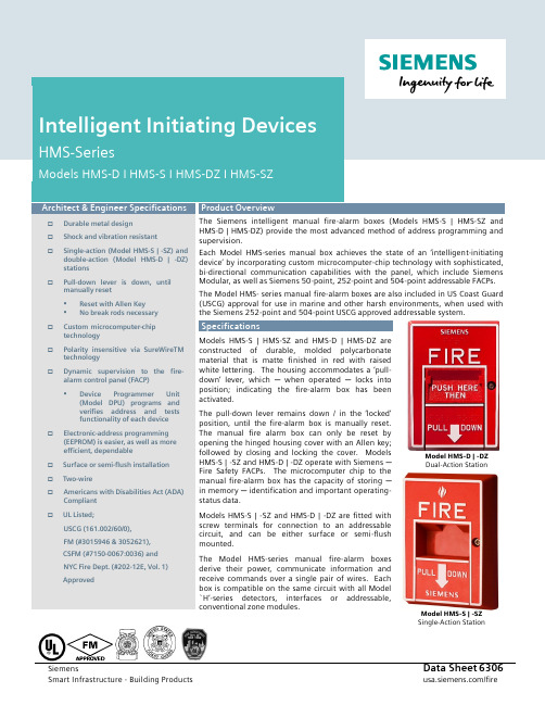
Intelligent Initiating Devices HMS-SeriesModels HMS-D I HMS-S I HMS-DZ I HMS-SZArchitect & Engineer Specifications☐Durable metal design☐Shock and vibration resistant☐Single-action (Model HMS-S | -SZ) and double-action (Model HMS-D | -DZ)stations☐Pull-down lever is down, untilmanually reset▪Reset with Allen Key▪No break rods necessary☐Custom microcomputer-chiptechnology☐Polarity insensitive via SureWireTM technology☐Dynamic supervision to the fire-alarm control panel (FACP)▪Device Programmer Unit(Model DPU) programs andverifies address and testsfunctionality of each device☐Electronic-address programming(EEPROM) is easier, as well as moreefficient, dependable☐Surface or semi-flush installation☐Two-wire☐Americans with Disabilities Act (ADA) Compliant☐UL Listed;USCG (161.002/60/0),FM (#3015946 & 3052621),CSFM (#7150-0067:0036) andNYC Fire Dept. (#202-12E, Vol. 1)Approved Product OverviewThe Siemens intelligent manual fire-alarm boxes (Models HMS-S | HMS-SZ and HMS-D | HMS-DZ) provide the most advanced method of address programming and supervision.Each Model HMS-series manual box achieves the state of an ‘intelligen t-initiating device’ by incorporating custom microcomputer-chip technology with sophisticated, bi-directional communication capabilities with the panel, which include Siemens Modular, as well as Siemens 50-point, 252-point and 504-point addressable FACPs. The Model HMS- series manual fire-alarm boxes are also included in US Coast Guard (USCG) approval for use in marine and other harsh environments, when used with the Siemens 252-point and 504-point USCG approved addressable system.SpecificationsModels HMS-S | HMS-SZ and HMS-D | HMS-DZ areconstructed of durable, molded polycarbonatematerial that is matte finished in red with raisedwhite lettering. The housing accommodates a ‘pull-down’ lever, which ─when operated ─locks intoposition; indicating the fire-alarm box has beenactivated.The pull-down lever remains down / in the ‘locked’position, until the fire-alarm box is manually reset.The manual fire alarm box can only be reset byopening the hinged housing cover with an Allen key;followed by closing and locking the cover. ModelsHMS-S | -SZ and HMS-D | -DZ operate with Siemens ─Fire Safety FACPs. The microcomputer chip to themanual fire-alarm box has the capacity of storing ─in memory ─ identification and important operating-status data.Models HMS-S | -SZ and HMS-D | -DZ are fitted withscrew terminals for connection to an addressablecircuit, and can be either surface or semi-flushmounted.The Model HMS-series manual fire-alarm boxesderive their power, communicate information andreceive commands over a single pair of wires. Eachbox is compatible on the same circuit with all Model`H’-series detectors, interfaces or addressable,conventional zone modules.Model HMS-D | -DZDual-Action StationModel HMS-S | -SZSingle-Action StationMounting DiagramDevice / Programmer Tester – Model DPUInnovative technology from Siemens ─ Fire Safety also allows all Model HMS-series intelligent manual fire-alarm boxes to be programmed via the Device Programmer / Test Unit (Model DPU). The programmer / tester is a compact, portable and menu-driven accessory that makes programming and testing of a manual fire-alarm box device faster, easier and more dependable than previous methods.Model DPU eliminates the need for mechanical-addressing mechanisms of a device because Model DPU electronically sets the address of the manual fire-alarm box into its microcomputer chip, non-volatile memory. Therefore, vibration, corrosion and other conditions -- which can compromise the functionality of mechanical-addressing mechanisms – are no longer an issue.Technical Data+ denotes (C)ountry (O)f (O)riginMODELOR TYPEPART NUMBERPRODUCTSHIPPING WEIGHTHMS-D 500-033400Addressable Manual Fire Alarm Box, Dual Action2.5 Lbs. 1.13 0z. HMS-DZ S54321-F5-A1Addressable Manual Fire Alarm Box, Dual Action[C.O.O. + – USA]HMS-S 500-033200Addressable Manual Fire Alarm Box, Single Action2.0 Lbs. 0.9 0z. HMS-SZ S54321-F6-A1Addressable Manual Fire Alarm Box, Single Action[C.O.O. + – USA] LTP 500-620490 Reset Tool Package [contains two (2) tools] 0.5 Lb. 0.23 0z. SB-5R310-019860Surface-Mounting Box 1.5 Lbs. 0.7 0z.ELECTRICALCurrent Draw (Active or Standby)0.9mAINDOOR / DRY CONDITIONSOperating Temperature Range 32° ─ 100°F (0° ─ 38°C) Operating Humidity Range 0 ─ 93%, non-condensingDetails for OrderingN OT I CE–The information contained in this data-sheet document is intended only as a summary, and is subject to change without notice.The product(s) described here has/have a specific instruction sheet(s)that cover various technical, limitation and liability information.Copies of install-type, instruction sheets – as well as the GeneralProduct Warning and Limitations document, which also containsimportant data, are provided with the product. All are availablefrom the Manufacturer.Data contained in the aforesaid type of documentation should be consultedwith a fire-safety professional before specifying or using the product.Any further questions or assistance concerningparticular problems that might arise, relative to theproper functioning of the equipment, please contact the Manufacturer.Siemens Industry, Inc.Smart Infrastructure - Building Products 8 Fernwood Road • Florham Park, NJ 07932Tel: (973) 593-2600July - 2019(Rev. 10 )。
大型游戏机厂家使用说明书

-4-
概述
检查机器出厂包装件 包装清单:本产品包装为一个整体,打开包装后即可插电使用。
请注意
● 请仔细确认包装附件是否齐备 ● 如有缺货情况发生,请及时与经销店及货运承担商联系。
-5-
机台功能简介
整机前面部分介绍
-6-
机台功能简介
内部线路连接示意图
-1-
前言
感谢您购买本公司出品的“3D 索尼克”(以下简称“本机”)产品,在使用本 产品之前,请认真阅读本说明书。当您开始使用本产品时,我们认为您已经认真 阅读了本说明书。使用说明书的所有内容均是通过本公司细心编写,如有任何印 刷错漏或翻译错误望广大用户谅解。当本机软件如需升级时,涉及的内容有所改 变时,恕不另行通知,请谅解。 本说明书的部份图片是在开发阶段设计的,可能与实物略有不同,但不会影响用 户使用。 在本使用说明书中说明了以下内容: ● 安全地进行本机的搬运、安装、移动、运行、设置、维护、废弃方法。 ● 为充分运用本机的功能详细提供了游戏设置、玩法。 ● 为确保使用本机的玩家以及在周围参观的人士的安全的方法。 ● 关于本机简易故障排除和本机修理的方法。 ● 关于本机操作或维修的疑问,请向我司经销店或客户服务中心咨询。
清扫脏污
注意
● 不要使用如酒精和丙酮等有机溶剂,用于清洗。有机溶剂可导致材料损耗。 ● 不要使用碱性或酸性的清洁剂。
本游戏每关有四个难度,每次必须跑在第一才能进入下一难度,如在规定时间内 未完成或完成了但不是第一名都将失败。
- 17 -
游戏玩法
42 寸 3D 高清液晶显示器,冲击您的视觉感观。 时尚外观设计、新颖独特。动感方向盘和坐椅,让你身临其境。满足您的人性化需求。 14 个游戏人物和汽车、5 个难度模式、6 个地图、随你选择。晋级模式,15 个晋级关卡. 新滚轮设计,移动方便快捷。 为方便顾客使用,本游戏设有 3D/2D 切换功能键,游戏者可根据自己需要手动调节。 该游戏为新型摸拟游戏,与其它模拟游戏相比较,这款游戏更具有动漫艺术气息。新增的游戏道具,主游戏更刺 激。 本游戏通过定时和任务模式同时进行游戏,不仅要在规定时间内完成,还要是参赛选手中最优秀的才能通关。 玩家每关都有三条生命,请好好珍惜哦。 本游戏通过计时和任务晋级,时间耗尽即游戏结束,任务未完成,游戏结束。只有在规定时间内完成任务才能进 入下一游戏关卡。游戏中共有八名选手一起游戏,你是其中一员,游戏结过关或结束时系统会对所有游戏选手的 表现进行排名
MAX8864T中文资料

GND 2
MAX8863 MAX8864
OUT
IN 3
4
SOT23-5
Dual Mode is a trademark of Maxim Integrated Products.
________________________________________________________________ Maxim Integrated Products 1
ELECTRICAL CHARACTERISTICS
(VIN = +3.6V, GND = 0V, TA = TMIN to TMAX, unless otherwise noted. Typical values are at TA = +25°C.) (Note 1) PARAMETER Input Voltage (Note 2) Output Voltage Adjustable Output Voltage Range (Note 3) Maximum Output Current Current Limit (Note 4) Ground Pin Current Dropout Voltage (Note 5) Line Regulation Load Regulation Output Voltage Noise SHUTDOWN SHDN Input Threshold SHDN Input Bias Current Shutdown Supply Current Shutdown to Output Discharge Delay (MAX8864) VIH VIL ISHDN IQSHDN V SHDN = VIN VOUT = 0V COUT = 1µF, no load TA = +25°C TA = TMAX TA = +25°C TA = TMAX 0 0.05 0.08 20 1 50 2.0 0.4 2.5 V nA nA ms ∆VLNR ∆VLDR ILIM IQ SET = GND IOUT = 1mA IOUT = 50mA VIN = 2.5V to 5.5V, SET tied to OUT, IOUT = 1mA IOUT = 0mA to 50mA 10Hz to 1MHz SET = GND SET tied to OUT COUT = 1µF COUT = 100µF -0.10 ILOAD = 0mA ILOAD = 50mA SYMBOL VIN VOUT 0mA ≤ IOUT ≤ 50mA, SET = GND MAX886_T MAX886_S MAX886_R VOUT CONDITIONS MIN 2.5 3.05 2.75 2.70 VSET 100 220 68 80 1.1 55 0 0.011 0.006 350 220 120 0.10 0.040 150 3.15 2.84 2.80 TYP MAX 5.5 3.25 2.93 2.88 5.5 V mA mA µA mV %/V %/mA µVRMS V UNITS V
MAX6314US29D2+T 微处理器监控电源供应电路说明书

RELIABILITY REPORTFORMAX6314US29D2+TPLASTIC ENCAPSULATED DEVICESOctober 11, 2010MAXIM INTEGRATED PRODUCTS120 SAN GABRIEL DR.SUNNYVALE, CA 94086Approved byDon LippsQuality AssuranceManager, Reliability EngineeringConclusionThe MAX6314US29D2+T successfully meets the quality and reliability standards required of all Maxim products. In addition, Maxim"s continuous reliability monitoring program ensures that all outgoing product will continue to meet Maxim"s quality and reliability standards.Table of ContentsI. ........Device Description V. ........Quality Assurance InformationII. ........Manufacturing Information VI. .......Reliability EvaluationIII. .......Packaging Information IV. .......Die Information.....AttachmentsI. Device DescriptionA. GeneralThe MAX6314 low-power CMOS microprocessor (µP) supervisory circuit is designed to monitor power supplies in µP and digital systems. TheMAX6314's active-low RESET output is bidirectional, allowing it to be directly connected to µPs with bidirectional reset inputs, such as the 68HC11. It provides excellent circuit reliability and low cost by eliminating external components and adjustments. The MAX6314 also provides a debounced manual reset input. This device performs a single function: it asserts a reset signal whenever the VCC supply voltage falls below a preset threshold or whenever manual reset is asserted. Reset remains asserted for an internally programmed interval (reset timeout period) after VCC has risen above the reset threshold or manual reset is deasserted. The MAX6314 comes with factory-trimmed reset threshold voltages in 100mV increments from2.5V to 5V. Preset timeout periods of 1ms, 20ms, 140ms, and 1120ms (minimum) are also available. The device comes in a SOT143 package. For a µP supervisor with an open-drain reset pin, see the MAX6315 data sheet.A. Description/Function: 68HC11/Bidirectional-Compatible µP Reset CircuitB. Process: B12C. Number of Device Transistors:D. Fabrication Location: Oregon or TexasE. Assembly Location: Malaysia, ThailandF. Date of Initial Production: Pre 1997III. Packaging InformationA. Package Type: 4-pin SOTB. Lead Frame: Alloy42C. Lead Finish: 100% matte TinD. Die Attach: ConductiveE. Bondwire: Au (1 mil dia.)F. Mold Material: Epoxy with silica fillerG. Assembly Diagram: #05-1601-0015H. Flammability Rating: Class UL94-V0Level 1I. Classification of Moisture Sensitivity perJEDEC standard J-STD-020-CJ. Single Layer Theta Jb: 250*°C/WK. Single Layer Theta Jc: 130°C/WL. Multi Layer Theta Ja: N/AM. Multi Layer Theta Jc: N/AIV. Die InformationA. Dimensions: 40 X 31 milsB. Passivation: Si3N4/SiO2 (Silicon nitride/ Silicon dioxide)C. Interconnect: Al/0.5%Cu with Ti/TiN BarrierD. Backside Metallization: NoneE. Minimum Metal Width: 1.2 microns (as drawn)F. Minimum Metal Spacing: 1.2 microns (as drawn)G. Bondpad Dimensions: 5 mil. Sq.H. Isolation Dielectric: SiO2I. Die Separation Method: Wafer Saw= 1= 1.83 (Chi square value for MTTF upper limit) MTTF 192 x 4340 x 443 x 2 (where 4340 = Temperature Acceleration factor assuming an activation energy of 0.8eV) A. Quality Assurance Contacts:Don Lipps (Manager, Reliability Engineering) Bryan Preeshl (Vice President of QA)B. Outgoing Inspection Level: 0.1% for all electrical parameters guaranteed by the Datasheet.0.1% For all Visual Defects.C. Observed Outgoing Defect Rate: < 50 ppmD. Sampling Plan:Mil-Std-105DVI. Reliability EvaluationA. Accelerated Life Test The results of the 135°C biased (static) life test are shown in Table 1. Using these results, the Failure Rate ( ) is calculated as follows:= 2.5 x 10-9= 2.5 F.I.T. (60% confidence level @ 25°C)The following failure rate represents data collected from Maxim"s reliability monitor program. Maxim performs quarterly life test monitors on its processes. This data is published in the Reliability Report found at /qa/reliability/monitor. ***********************************************************************@55C(0.8eV,60%UCL)B. E.S.D. and Latch-Up Testing (lot BNMAAA004GZ, D/C 9801)The MS11 die type has been found to have all pins able to withstand a HBM transient pulse of +/-2000V per Mil-Std 883 Method 3015.7. Latch-Up testing has shown that this device withstands a current of +/-250mA and overvoltage per JEDEC JESD78.Table 1Reliability Evaluation Test Results MAX6314US29D2+TTEST ITEM TEST CONDITION FAILUREIDENTIFICATION SAMPLE SIZE NUMBER OF COMMENTSFAILURESStatic Life Test (Note 1)Ta = 135°C BiasedTime = 192 hrs. DC Parameters& functionality49 0SNMBGQ001D,DC034580 0 INMBEQ001CQ, DC 991480 0NNMBDX001F,DC974177 0BNMBAB007K,DC970480 0BNMBAO001B,DC962377 0BNMAAB006L,DC9704Note 1: Life Test Data may represent plastic DIP qualification lots.。
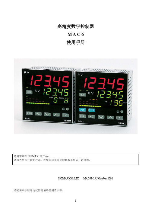
MAC6中文说明书
3-3 订货信息
项目 型号 输入
代码 MAC6A-
调节输出 1
电源
规格 96×96mm 5 位数字显示高精度字控制器 M 自由输入、TC、RTD、mV、V、mA
C 继电器接点 1a 240V AC 2A( 阻性负载 ) S 固态继电器(SSR)驱动 12V DC 最大20mA I 电流 4-20mA DC 负载电阻最大500Ω V 电压 0-10V DC 负载电流最大2mA Y 控制电机 (伺服控制输出)接点容量1C 240V AC 2A X 控制电机 (伺服控制输出)SSR 240V AC 2A
3
生电磁干扰。请在采取有效措施后使用。 ● 仪器具有用于散热的通风口,并且确保金属不会进入通风口中,否则会引起故障或者火灾。 ● 不要阻塞通风口或者使尘埃和其他类似物附着在上面,温度升高或者绝缘失效都会缩短产品寿命并
引起火灾。 ● 应该注意在重复性极限值(如电压、噪声、浪涌)实验时可能会损坏设备。 ● 禁止使用者改型和不正当使用。 3 简介 3-1 使用前的检查
在使用 MAC6 前请检查型号代码、外观和附件。确认没有错误、损坏和丢失。 确认型号代码,检查与订货的产品一致。根据下述代码表检查机壳上的型号代码。 检查附件 「注」 如果您有任何问题请联系我们的代理商或者营业本部。我们欢迎任何询问,例如,产品缺
陷、附件丢失等。
「 注意 」
3-2 使用注意事项 ●不要用硬的、尖的物体操作前面板。不要用指甲尖触碰按键。 ●当清洁仪器时,用干布轻擦。不要使用溶剂,如,稀释剂。
7. 功能的补充说明・・・・・・・・・・・・・・・・・・・・・・・・・・・・・・・・・・・・・・・・・・・・・・・・・・・・・・・・・・・・・・・60
7-1 自动返回功能・・・・・・・・・・・・・・・・・・・・・・・・・・・・・・・・・・・・・・・・・・・・・・・・・・・・・・・・・・・・・60 7-2 输出软启动功能・・・・・・・・・・・・・・・・・・・・・・・・・・・・・・・・・・・・・・・・・・・・・・・・・・・・・・・・・・・60 7-3 事件报警方式・・・・・・・・・・・・・・・・・・・・・・・・・・・・・・・・・・・・・・・・・・・・・・・・・・・・・・・・・・・・・60 7-4 AT(自整定)・・・・・・・・・・・・・・・・・・・・・・・・・・・・・・・・・・・・・・・・・・・・・・・・・・・・・・・・・・・・・60
- 1、下载文档前请自行甄别文档内容的完整性,平台不提供额外的编辑、内容补充、找答案等附加服务。
- 2、"仅部分预览"的文档,不可在线预览部分如存在完整性等问题,可反馈申请退款(可完整预览的文档不适用该条件!)。
- 3、如文档侵犯您的权益,请联系客服反馈,我们会尽快为您处理(人工客服工作时间:9:00-18:30)。
General DescriptionThe MAX6305–MAX6313 CMOS microprocessor (µP)supervisory circuits are designed to monitor more than one power supply. Ideal for monitoring both 5V and 3.3V in personal computer systems, these devices assert a system reset if any of the monitored supplies falls outside the programmed threshold. Low supply current (15µA) and a small package suit them for portable applications. The MAX6305–MAX6313 are specifically designed to ignore fast transients on any monitored supply.These devices are available in a SOT23-5 package,have factory-programmed reset thresholds from 2.5V to 5.0V (in 100mV increments), and feature four power-on reset timeout periods. Ten standard versions are avail-able. Contact the factory for availability of non standard versions.ApplicationsPortable Computers Computers ControllersIntelligent InstrumentsPortable/Battery-Powered Equipment Multivoltage Systems: 3V/5V, 5V/12V, 5V/24V Embedded Control SystemsFeatureso Small 5-Pin SOT23 Packageo Precision Factory-Set V CC Reset Thresholds;Available in 0.1V Increments from 2.5V to 5V o Immune to Short V CC Transientso Guaranteed RESET Valid to V CC = 1V o Guaranteed Over Temperature o 8µA Supply Currento Factory-Set Reset Timeout Delay from 1ms (min) to 1120ms (min)o No External Components o Manual Reset Inputo Under/Overvoltage Supply MonitoringMAX6305–MAX63135-Pin, Multiple-Input,Programmable Reset ICs________________________________________________________________Maxim Integrated Products119-1145; Rev 5; 4/08†The MAX6306/MAX6307/MAX6309/MAX6310/MAX6312/MAX6313 are available with factory-set V CC reset thresholds from 2.5V to 5V, in 0.1V increments. Insert the desired nominal reset threshold (from Table 1) into the blanks following the letters UK.All parts also offer factory-programmed reset timeout periods.Insert the number corresponding to the desired nominal timeout period index following the “D” in the part number (D1 = 1ms min,D2 = 20ms min, D3 = 140ms min, and D4 = 1120ms min). There are 10 standard versions with a required order increment of 2,500pieces. Sample stock is generally held on the standard versions only (see Standard Versions table). Required order increment is 10,000 pieces for non-standard versions. Contact factory for availability of non-standard versions. All devices available in tape-and-reel only.Devices are available in both leaded and lead-free packaging.Specify lead-free by replacing “-T” with “+T” when ordering.Pin Configurations and Typical Operating Circuit appear atend of data sheet.Ordering Information continued at end of data sheet.Standard Versions Table appears at end of data sheet._______________________________________________________________Selector TableFor pricing, delivery, and ordering information, please contact Maxim Direct at 1-888-629-4642,or visit Maxim’s website at .M A X 6305–M A X 63135-Pin, Multiple-Input, Programmable Reset ICsABSOLUTE MAXIMUM RATINGSELECTRICAL CHARACTERISTICSV CC = +2.5V to +5.5V for the MAX6305/MAX6308/MAX6311, V CC = (V TH + 2.5%) to +5.5V for the MAX6306/MAX6307/MAX6309/Stresses beyond those listed under “Absolute Maximum Ratings” may cause permanent damage to the device. These are stress ratings only, and functional operation of the device at these or any other conditions beyond those indicated in the operational sections of the specifications is not implied. Exposure to absolute maximum rating conditions for extended periods may affect device reliability.V CC ...........................................................................-0.3V to +6V All Other Pins..............................................-0.3V to (V CC + 0.3V)Input/Output Current, All Pins.............................................20mA Rate of Rise, V CC ............................................................100V/µs Continuous Power Dissipation (T A = +70°C)SOT23-5 (derate 7.1mW/°C above +70°C).................571mWOperating Temperature RangeMAX63_ _UK _ _D_-T.........................................0°C to +70°C MAX63_ _EUK _ _D_-T...................................-40°C to +85°C Storage Temperature Range.............................-65°C to +160°C Lead Temperature (soldering, 10sec).............................+300°CMAX6305–MAX63135-Pin, Multiple-Input, Programmable Reset ICs_______________________________________________________________________________________3ELECTRICAL CHARACTERISTICS (continued)V CC = +2.5V to +5.5V for the MAX6305/MAX6308/MAX6311, V CC = (V TH + 2.5%) to +5.5V for the MAX6306/MAX6307/MAX6309/Note 2: The MAX6305/MAX6308/MAX6311 switch from undervoltage reset to normal operation between 1.5V < V CC < 2.5V.Note 3: The MAX6306/MAX6307/MAX6309/MAX6310/MAX6312/MAX6313 monitor V CC through an internal factory-trimmed voltagedivider, which programs the nominal reset threshold. Factory-trimmed reset thresholds are available in approximately 100mV increments from 2.5V to 5V (Table 1).Note 4:Guaranteed by design.M A X 6305–M A X 63135-Pin, Multiple-Input, Programmable Reset ICs 4_________________________________________________________________________________________________________________________________Typical Operating Characteristics(V CC = +5V, T A = +25°C, unless otherwise noted.)5.05.56.06.57.07.58.08.59.09.5-60-40-2020406080100SUPPLY CURRENT vs. TEMPERATURETEMPERATURE (°C)S U P P L Y C U R R E N T (μA )01020304050607080-60-40-2020406080100V CC FALLING PROPAGATION DELAYvs. TEMPERATURETEMPERATURE (°C)P R O P A G A T I O N D E L A Y (n s )010203040506070-60-40-20020406080100OVRST IN RISING PROPAGATION DELAY vs. TEMPERATURE (OVERVOLTAGE RESET INPUT)TEMPERATURE (°C)P R O P A G A T I O N D E L A Y (n s )020406080100120-60-40-2020406080100RST IN_ FALLING PROPAGATION DELAY vs. TEMPERATURETEMPERATURE (°C)R S T I N _ P R O P A G A T I O N D E L A Y (n s )104001200800MAXIMUM TRANSIENT DURATION vs.VCC RESET THRESHOLD OVERDRIVE10OVERDRIVE, V TH - V CC (mV)T R A N S I E N T D U R A T I O N (μs )100100010,0000.900.920.940.960.981.001.021.041.061.081.10-60-40-20020406080100RESET TIMEOUT vs. TEMPERATURE6305 T O C 05TEMPERATURE (°C)N O R M A L I Z E D R E S E T T I M E O U T0.9900.9920.9940.9960.9981.0001.0021.0041.0061.0081.010-60-40-2020406080100RESET THRESHOLD vs. TEMPERATURE6305 T O C 06TEMPERATURE (°C)N O R M A L I Z E D R E S E T T H R E S H O L D (V /V )104001200800MAXIMUM TRANSIENT DURATION vs.OVRST IN THRESHOLD OVERDRIVE10OVERDRIVE, V OVRST IN - V REF (mV)T R A N S I E N T D U R A T I O N (μs )100100010,000104001200800MAXIMUM TRANSIENT DURATION vs.RST IN_ THRESHOLD OVERDRIVE10OVERDRIVE, V REF - V RST IN (mV)T R A N S I E N T D U R A T I O N (μs )100100010,000_______________Detailed DescriptionThe MAX6305–MAX6313 CMOS microprocessor (µP)supervisory circuits are designed to monitor more than one power supply and issue a system reset when any monitored supply falls out of regulation. The MAX6305/MAX6308/MAX6311 have two adjustable undervoltage reset inputs (RST IN1 and RST IN2). The MAX6306/MAX6307/MAX6309/MAX6310/MAX6312/MAX6313 mon-itor V CC through an internal, factory-trimmed voltage divider. The MAX6306/MAX6309/MAX6312 have, in addition, an adjustable undervoltage reset input and a manual-reset input. The internal voltage divider sets the reset threshold as specified in the device part number (Table 1). The MAX6307/MAX6310/ MAX6313 feature an adjustable undervoltage reset input (RST IN) and an adjustable overvoltage reset input (OVRST IN) in addition to the factory-trimmed reset threshold on the V CC moni-tor. Program the adjustable reset inputs with an external resistor divider (see Adjustable Reset Inputs section).Reset OutputsA µP’s reset input starts the µP in a known state. These µP supervisory circuits assert reset to prevent code-execution errors during power-up, power-down, or brownout conditions.RESET (MAX6305–MAX6310) and RESET (MAX6311/MAX6312/MAX6313) are guaranteed to be asserted at a valid logic level for V CC > 1V (see Electrical Characteristics ). Once all monitored voltages exceed their programmed reset thresholds, an internal timer keeps reset asserted for the reset timeout period (t RP );after this interval, reset deasserts.If a brownout condition occurs (any or all monitored volt-ages dip outside their programmed reset threshold),reset asserts (RESET goes high; RESET goes low). Any time any of the monitored voltages dip below their reset threshold, the internal timer resets to zero and reset asserts. The internal timer starts when all of the moni-tored voltages return above their reset thresholds, and reset remains asserted for a reset timeout period. The MAX6305/MAX6306/MAX6307 feature an active-low,MAX6305–MAX63135-Pin, Multiple-Input, Programmable Reset ICs_______________________________________________________________________________________5______________________________________________________________Pin DescriptionM A X 6305–M A X 6313open-drain, N-channel output. The MAX6308/MAX6309/MAX6310 feature an active-low, complementary output structure that both sinks and sources current, and the MAX6311/MAX6312/MAX6313 have an active-high com-plementary reset output.The MAX6305/MAX6308/MAX6311 switch from under-voltage lockout operation to normal operation between 1.5V < V CC < 2.5V. Below 1.5V, V CC undervoltage-lockout mode asserts RESET . Above 2.5V, V CC normal-operation mode asserts reset if RST IN_ falls below the RST IN_ threshold.Manual-Reset Input(MAX6306/MAX6309/MAX6312)Many µP-based products require manual-reset capability,allowing an operator or external logic circuitry to initiate a reset. A logic low on MR asserts reset. Reset remains asserted while MR is low, and for a reset active timeout period (t RP ) after MR returns high. This input has an inter-nal 63.5k Ωpull-up resistor, so it can be left open if it is not used. MR can be driven with TTL-logic levels in 5V sys-tems, with CMOS-logic levels in 3V systems, or with open-drain/collector output devices. Connect a normally open momentary switch from MR to GND to create a manual-reset function; external debounce circuitry is not required.If MR is driven from long cables or if the device is used in a noisy environment, connecting a 0.1µF capacitor from MR to ground provides additional noise immunity.The MR pin has internal ESD-protection circuitry that may be forward biased under certain conditions, drawing excessive current. For example, assume the circuitry driv-ing MR uses a +5V supply other than V CC . If V CC drops or browns out lower than +4.7V, MR ’s absolute maximum rat-ing is violated (-0.3V to (V CC + 0.3V)), and undesirable current flows through the ESD structure from MR to V CC .To avoid this, it is recommended that the supply for the MR pin be the same as the supply monitored by V CC . In this way, the voltage at MR will not exceed V CC .Adjustable Reset InputsThe MAX6305–MAX6313 each have one or more reset inputs (RST IN_ /OVRST IN). These inputs are com-pared to the internal reference voltage (F igure 1).Connect a resistor voltage divider to RST IN_ such that V RST IN_falls below V RSTH (1.23V) when the monitored voltage (V IN ) falls below the desired reset threshold (V TH ) (F igure 2). Calculate the desired reset voltage with the following formula:R1 + R2V TH = ________x VRSTHR25-Pin, Multiple-Input, Programmable Reset ICs 6_______________________________________________________________________________________Figure 1. Functional DiagramMAX6305–MAX63135-Pin, Multiple-Input, Programmable Reset ICs_______________________________________________________________________________________7The ±25nA max input leakage current allows resistors on the order of megohms. Choose the pull-up resistor in the divider to minimize the error due to the input leakage cur-rent. The error term in the calculated threshold is simply:±25nA x R1If you choose R1 to be 1M Ω, the resulting error is ±25 x 10-9x 1 x 106= ±25mV.Like the V CC voltage monitors on the MAX6306/MAX6307/MAX6309/MAX6310/MAX6312/MAX6313, the RST IN_inputs (when used with a voltage divider) are designed to ignore fast voltage transients. Increase the noise immunity by connecting a capacitor on the order of 0.1µF between RST IN and GND (Figure 2). This creates a single-pole lowpass filter with a corner frequency given by:f = (1/2π) / (R1 + R2)(R1 x R2 x C)For example, if R1 = 1M Ωand R2 = 1.6M Ω, adding a 0.1µF capacitor from RST IN_ to ground results in a lowpass corner frequency of f = 2.59Hz. Note that adding capacitance to RST IN slows the circuit’s overall response time.__________Applications InformationInterfacing to µPs with Bidirectional Reset PinsSince the RESET output on the MAX6305/MAX6306/MAX6307 is open drain, these devices interface easily with µPs that have bidirectional reset pins, such as the Motorola 68HC11. Connecting the µP supervisor’s RESET output directly to the microcontroller’s RESET pin with a single pull-up resistor allows either device to assert reset (Figure 3).Negative-Going V CC TransientsIn addition to issuing a reset to the µP during power-up,power-down, and brownout conditions, these devices are relatively immune to short-duration, negative-going V CC transients (glitches).The Typical Operating Characteristics show the Maximum Transient Duration vs. V CC Reset Threshold Overdrive, for which reset pulses are not generated.The graph was produced using negative-going pulses,starting at V TH max, and ending below the pro-grammed reset threshold by the magnitude indicated (reset threshold overdrive). The graph shows the maxi-mum pulse width that a negative-going V CC transient may typically have without causing a reset pulse to be issued. As the amplitude of the transient increases (i.e.,goes farther below the reset threshold), the maximum allowable pulse width decreases.RST IN_/OVRST IN are also immune to negative/positive-going transients (see Typical Operating Characteristics ).A 0.1µF bypass capacitor mounted close to the RST IN_,OVRST IN, and/or the V CC pin provides additional tran-sient immunity.Ensuring a Valid RESET /RESETOutput Down to V CC = 0VWhen V CC falls below 1V, push/pull structured RESET /RESET current sinking (or sourcing) capabilities decrease drastically. High-impedance CMOS-logic inputs connected to RESET can drift to undetermined voltages. This presents no problem in most applica-tions, since most µPs and other circuitry do not operate with V CC below 1V. In those applications where RESET must be valid down to 0V, adding a pull-down resistor between RESET and ground sinks any stray leakageFigure 2. Increasing Noise ImmunityFigure 3. Interfacing to µPs with Bidirectional Reset I/Ocurrents, holding RESET low (Figure 4). The pull-down resistor’s value is not critical; 100k Ωis large enough not to load RESET and small enough to pull RESET to ground. For applications where RESET must be valid to V CC , a 100k Ωpull-up resistor between RESET and V CC will hold RESET high when V CC falls below 1V (Figure 5).Since the MAX6305/MAX6306/MAX6307 have open-drain, active-low outputs, they typically use a pull-up resistor. With these devices and under these conditions (V CC < 1V), RESET will most likely not maintain an active condition, but will drift toward a nonactive level due to the pull-up resistor and the RESET output’s reduction in sinking capability. These devices are not recommended for applications that require a valid RESET output below 1V.* Factory-trimmed reset thresholds are available in approximately 100mV increments with a ±1.5% room-temperature variance.M A X 6305–M A X 63135-Pin, Multiple-Input, Programmable Reset ICs 8_______________________________________________________________________________________Figure 4. Ensuring RESET Valid to V CC = 0VFigure 5. Ensuring RESET Valid to V CC = 0VTable 1. Factory-Trimmed Reset Thresholds*MAX6305–MAX63135-Pin, Multiple-Input, Programmable Reset ICs_______________________________________________________________________________________9Chip InformationTRANSISTOR COUNT: 800Typical Operating Circuit†The MAX6306/MAX6307/MAX6309/MAX6310/MAX6312/MAX6313 are available with factory-set V CC reset thresholds from 2.5V to 5V, in 0.1V increments. Insert the desired nominal reset threshold (from Table 1) into the blanks following the letters UK.All parts also offer factory-programmed reset timeout periods.Insert the number corresponding to the desired nominal timeout period index following the “D” in the part number (D1 = 1ms min,D2 = 20ms min, D3 = 140ms min, and D4 = 1120ms min). There are 10 standard versions with a required order increment of 2,500pieces. Sample stock is generally held on the standard versions only (see Standard Versions table). Required order increment is 10,000 pieces for non-standard versions. Contact factory for avail-ability of non-standard versions. All devices available in tape-and-reel only.Devices are available in both leaded and lead-free packaging.Specify lead-free by replacing “-T” with “+T” when ordering.M A X 6305–M A X 63135-Pin, Multiple-Input, Programmable Reset ICs 10______________________________________________________________________________________Pin ConfigurationsPackage InformationFor the latest package outline information, go to /packages .Maxim cannot assume responsibility for use of any circuitry other than circuitry entirely embodied in a Maxim product. No circuit patent licenses are implied. Maxim reserves the right to change the circuitry and specifications without notice at any time.Maxim Integrated Products, 120 San Gabriel Drive, Sunnyvale, CA 94086 408-737-7600 ____________________11©2008 Maxim Integrated Productsis a registered trademark of Maxim Integrated Products, Inc.MAX6305–MAX6313 5-Pin, Multiple-Input, Programmable Reset ICs元器件交易网。