KA337TU,KA337,KA337, 规格书,Datasheet 资料
BYW29-200G;中文规格书,Datasheet资料
0.5 1.0 2.0
5.0 10
20
t, TIME (ms)
Figure 6. Thermal Response
50 100 200
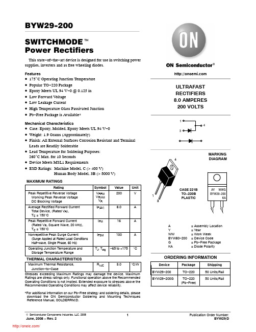
ULTRAFAST RECTIFIERS 8.0 AMPERES 200 VOLTS
1 4
3
MARKING
4
DIAGRAM
1 3
CASE 221B TO−220B PLASTIC
AY WWG BYW29-200
KA
A Y WW BYW80−200 G KA
= Assembly Location = Year = Work Week = Device Code = Pb−Free Package = Diode Polarity
2
IF(AV), AVERAGE FORWARD CURRENT (AMPS)
r(t), TRANSIENT THERMAL RESISTANCE (NORMALIZED)
BYW29−200
PF(AV), AVERAGE POWER DISSIPATION (WATTS)
*For additional information on our Pb−Free strategy and soldering details, please download the ON Semiconductor Soldering and Mounting Techniques Reference Manual, SOLDERRM/D.
KA5M0365RTU;KA5M0380RYDTU;KA5L0380RYDTU;KA5H0365RTU;KA5M0365RYDTU;中文规格书,Datasheet资料

Operating Junction Temperature. Operating Ambient Temperature. Storage Temperature Range.
Symbol
VDGR VGS IDM
ID ID EAS VCC,MAX VFB PD Derating TJ TA TSTG
VDGR VGS IDM
ID ID EAS VCC,MAX VFB PD Derating TJ TA TSTG
Note: 1. Repetitive rating: Pulse width limited by maximum junction temperature 2. L = 51mH, starting Tj = 25°C 3. L = 13μH, starting Tj = 25°C
Absolute Maximum Ratings
(Ta=25°C, unless otherwise specified)
Characteristic KA5H0365R, KA5M0365R, KA5L0365R Drain-Gate Voltage (RGS=1MΩ) Gate-Source (GND) Voltage Drain Current Pulsed (1) Continuous Drain Current (TC=25°C) Continuous Drain Current (TC=100°C) Single Pulsed Avalanche Energy (2) Maximum Supply Voltage Analog Input Voltage Range
KA5x03xx-SERIES
KA5H0365R, KA5M0365R, KA5L0365R KA5H0380R, KA5M0380R, KA5L0380R Fairchild Power Switch(FPS)
PA341DF,PA341CE,PA341DW, 规格书,Datasheet 资料

F < 60Hz
PA341CE RESISTANCE, junction to air
Full Temperature Range
PA341DF RESISTANCE,
Full Tempera-
junction to air (Note 7) ture Range
5/50 50/200
BIAS CURRENT, vs. supply
0.2/2
OFFSET CURRENT, initial (Note 6)
2.5/50 50/200
INPUT IMPEDANCE, DC
1011
INPUT CAPACITANCE
3
COMMON MODE, voltage range
-40
125
Units V mA mA W
V V °C °C °C °C
SPECIFICATIONS
Parameter
Test Conditions
(Note 1)
PA341CE, PA341DF Min Typ Max
INPUT
OFFSET VOLTAGE, initial
12
40
OFFSET VOLTAGE, vs. temperature (Note 3)
The PA341CE is packaged in a hermetically sealed 8-pin TO-3 package. The metal case of the PA341CE is isolated in excess of full supply voltage.
The PA341DF is packaged in a 24 pin PSOP (JEDEC MO-166) package. The metal heat slug of the PA341DF is isolated in excess of full supply voltage. The PA341DW is packaged in Apex Precision Power’s hermetic ceramic SIP package. The alumina ceramic isolates the die in excess of full supply voltage.
LM337T_NL中文资料

©2001 Fairchild Semiconductor CorporationRev. 1.0.0Features•Output current in excess of 1.5A•Output voltage adjustable between -1.2V and - 37V •Internal thermal overload protection •Internal short circuit current limiting •Output transistor safe area compensation•Floating operation for high voltage applications •Standard 3-pin TO-220 packageDescriptionThe LM337 is a 3-terminal negative adjustable regulator. It supplies in excess of 1.5A over an output voltage range of -1.2V to - 37V . This regulator requires only two external resistor to set the output voltage. Included on the chip are current limiting, thermal overload protection and safe area compensation.TO-2201. Adj2. Input3. Output1LM3373-Terminal 1.5A Negative Adjustable RegulatorLM3372Absolute Maximum RatingsElectrical Characteristics(V I - V O = 5V, I O = 40mA, 0°C ≤ T J ≤ +125°C, P DMAX = 20W, unless otherwise specified)Note:1. Load and line regulation are specified at constant junction temperature. Change in V O due to heating effects must be taken intoaccount separately. Pulse testing with low duty is used.2. C ADJ , when used, is connected detween the adjustment pin and ground.ParameterSymbol Value Unit Input-Output Voltage Differential |V I - V O |40V Power DissipationP D Internally limitedW Operating Temperature Range T OPR 0 ~ +125°C Storage Temperature RangeT STG-65 ~+125°CParameterSymbolConditionsMin Typ.Max.Unit Line Regulation (Note1)R line T A = +25°C3V ≤ I V I - V O I ≤ 40V -0.010.04%/ V3V ≤ I V I - V O I ≤ 40V -0.020.07Load Regulation (Note1)R loadT A = +25°C10mA ≤ I O ≤ 0.5A -1550mV10mA ≤ I O ≤ 1.5A-15150Adjustable Pin Current I ADJ --50100µA Adjustable Pin Current Change∆I ADJT A =+ 25°C10mA ≤ I O ≤ 1.5A 3V ≤I V I - V O I ≤ 40V -25µA T A =+ 25°C-1.213-1.250-1.287Reference Voltage V REF 3V ≤ I V I - V O I ≤ 40V 10mA ≤ I O ≤ 1.5A -1.200-1.250-1.300V Temperature StabilityST T 0°C ≤ ΤJ ≤ +125°C -0.6-%Minimum Load Current to Maintain Regulation I L(MIN)3V ≤I V I - V O I ≤ 40V - 2.5103V ≤I V I - V O I ≤ 10V - 1.56mA Output Noisee N T A =+25°C 10Hz ≤f ≤10KHz -0.003-V/106Ripple Rejection Ratio RR V O = -10V, f = 120Hz -60-C ADJ = 10µF (Note2)6677-dB Long Term StabilityST T J = 125°C ,1000Hours-0.31%Thermal Resistance Junction to CaseR θJC--4-°C/ WLM337 Typical ApplicationFigure 1.Programmable Regulator•Ci is required if regulator is located more then 4 inches from power supply filter.A 1.0µF solid tantalum or 10µF aluminum electrolytic is recommended.Co is necessary for stability. A 1.0µF solid tantalum or 10µF aluminum electrolytic is recommended.•V O= -1.25V (1+R2/R1)3LM3374Mechanical DimensionsPackage4.50 ±0.209.90 ±0.201.52 ±0.100.80 ±0.102.40 ±0.2010.00 ±0.201.27 ±0.10ø3.60 ±0.10(8.70)2.80 ±0.1015.90 ±0.2010.08 ±0.3018.95M A X .(1.70)(3.70)(3.00)(1.46)(1.00)(45°)9.20 ±0.2013.08 ±0.201.30 ±0.101.30+0.10–0.050.50+0.10–0.052.54TYP [2.54 ±0.20]2.54TYP [2.54 ±0.20]TO-220LM337 Ordering InformationProduct Number Package Operating TemperatureLM337T TO-2200°C to + 125°C5LM3376/1/01 0.0m 001Stock#DSxxxxxxxx2001 Fairchild Semiconductor CorporationLIFE SUPPORT POLICYFAIRCHILD’S PRODUCTS ARE NOT AUTHORIZED FOR USE AS CRITICAL COMPONENTS IN LIFE SUPPORT DEVICES OR SYSTEMS WITHOUT THE EXPRESS WRITTEN APPROVAL OF THE PRESIDENT OF FAIRCHILD SEMICONDUCTOR CORPORATION. As used herein:1.Life support devices or systems are devices or systemswhich, (a) are intended for surgical implant into the body, or (b) support or sustain life, and (c) whose failure to perform when properly used in accordance with instructions for use provided in the labeling, can bereasonably expected to result in a significant injury of the user.2. A critical component in any component of a life supportdevice or system whose failure to perform can bereasonably expected to cause the failure of the life support device or system, or to affect its safety or effectiveness.DISCLAIMERFAIRCHILD SEMICONDUCTOR RESERVES THE RIGHT TO MAKE CHANGES WITHOUT FURTHER NOTICE TO ANY PRODUCTS HEREIN TO IMPROVE RELIABILITY, FUNCTION OR DESIGN. FAIRCHILD DOES NOT ASSUME ANYLIABILITY ARISING OUT OF THE APPLICATION OR USE OF ANY PRODUCT OR CIRCUIT DESCRIBED HEREIN; NEITHER DOES IT CONVEY ANY LICENSE UNDER ITS PATENT RIGHTS, NOR THE RIGHTS OF OTHERS.。
CG2145MS,CG2800MS,CG75MS,CG75LTR,CG2800LTR,CG2600LTR,CG2470L,CG75L, 规格书,Datasheet 资料

CG/CG2 Series
CG/CG2 Series
Description
Littelfuse highly reliable CG/CG2 Series GDTs provide a high degree of surge protection in a small size ideal for board level circuit protection. GDTs function as switches which dissipate a minimum amount of energy and therefore handle currents that far surpass other types of transient voltage protection. Their gas-filled, rugged ceramic metal construction make them well suited to adverse environments. The CG/CG2 series comes in a variety of forms including surface mount, core, straight and shaped leads, to serve a variety of mounting methods.
AGENCY FILE NUMBER
Agency Approvals
AGENCY
& &
2 Electrode GDT Graphical Symbol
The CG Series (75-110V) is ideal for protection of test and communication equipment and other devices in which low voltage limits and extremely low arc voltages are required. The CG2 Series (145V-1000V) is ideal for protecting equipment where higher voltage limits and holdover voltages are necessary.
KA334中文资料

0.5
-
%
-
160
-
°C
3
元器件交易网
KA334
Applications
< Tilt Coil Current Control Circuit in Monitor>
VCC
36kΩ
IN 10kΩ
6+
2
3
CH2
5-
4
VEE
9.1kΩ
40kΩ
7+
2
CH1
8-
4
1kΩ VEE
8-DIP
1
Internal Block Diagram
1 Vcc 2
3 VEE/GND 4
8 -
+
K
7
A
3
3
4
6
+
5
(8 DIP)
©2000 Fairchild Semiconductor International
Rev. 5.0
元器件交易网
KA334
PIN Definitions
Output Voltage Swing
Channel Separation Total Harmonic Distortion Thermal Shutdown Junction Temperature
Symbol VS
IS
Ib VOS IOS SR
B Ri GV eN IN CMRR PSRR
VO
Input Bias Current Input Offset Voltage Input Offset Current Slew Rate Gain-Bandwidth Product Input Resistance Lange Signal Input Noise Voltage Input Noise Current Common Mode Rejection Ratio Supply Voltage Rejection Ratio
0LEB00ABX,0LEB00BBX,0LEC00ABX,0LEC00BAX,0LEC00BBX,0LEB00BAX,0LEC00AAX, 规格书,Datasheet 资料

KLDR, KLKRBLF, BLN, FLM, FLQ, KLK, KLKD LEC/LEY series:Accepts only Littelfuse Class CC fuses:CCMRKLDR, KLKRWeb ResourcesSample requests, downloadable CAD drawings and other technical information: w /leb/lec /lex /ley /let• Sports lighting and various outdoor illuminated signs • Boat electrical circuits, tractors/yard equipment and general outdoor circuit protection (such as traffic signals, alley lighting and electric wheelchairs)SpecificationsVoltage rating: 600 V Ampere rating: 30 AInterrupting rating: 200 kA rms symmetrical (with Class CC fuses)Approvals: LEB/LEX series: UL Recognized Miscellaneous Fuseholder per UL UL 4248 (File No. E14721) CSA Certified per C22.2, No. 39 (File No. LR7316) LEC/LEY series: U L Listed Class CC BranchCircuitFuseholder per UL 512 (File No. E14721)CSA Certified per C22.2, No. 39 (File No. LR7316)Insulating Boots• Molded from engineering-grade thermoplastics, WPB1 and WPB3 boots provide high resistance to corrosive environments • WPB1 contains one standard boot for A, B, C, D or J terminations • WPB3 offers one Y -pole boot for use with Y -pole termination• For watertight protection of non-breakaway Y -pole termination, order one WPB1 and one WPB3 bootOrdering InformationTo order Littelfuse in-line fuseholders and disconnects by part number, refer to the charts on the next page.Re comme nde d Crimping T oolsThe following crimping tools or equivalents may be used on either the non-breakaway or breakaway watertight in-line fuseholders.LEB - AA - SLittelfuse SeriesLoad Side/Terminal SizeBreakaway FeatureLine Side/Terminal SizeDimensions in inches1-Pole1-Pole Breakaway2-PoleA &B Crimp TerminalC &D Crimp TerminalJ TerminalY TerminalOrdering Information (1-Pole LEB/LEC and 2-Pole LEX/LEY)Ordering Information (Solid Neutral LET Fuseholders)Ordering Information (Terminals)Two-Pole Breakaway HolderDescriptionNew Littelfuse LEXT-YY-S and LEX-YYC-S series breakaway fuseholders meet state and federal highway commission safety standards requiring fuseholders to readily disconnect from power in case of a pole knockdown.The breakaway feature consists of a receptacle permanently attached to the power line and a fuseholder with matching terminals. If a knockdown occurs, the parts separate, leaving the energized conductor recessed and unexposed.Features/Benefits• L EXT -YY version has a permanently installed “neutral” slug to prevent the neutral from accidentally being fused • L EX-YY version allows for fusing of line-to-line loads or other applications requiring two fuses to disconnect under strain • Fiberglass polymer body resists damage from impact • F our “Y” type set-screw terminals accommodate a wide range of solid and stranded Cu or Al conductors • O-ring and terminal boots form watertight seal, preventing leakageSpecificationsPart numbers: LEXT-YY-S (Solid neutral) LEX-YYC-S Voltage Rating:600VAC/VDC Ampere Rating:30AInterrupting Rating:200 kA with Class CC Fuses Y Terminals: Tin Plated Copper w/ set screws Wire Size: 1 solid #12 to #8 or1 stranded #10 to #2Approvals: UL Recognized (File E14721)CSA Certified (File LR7316)Applications• Street lighting • Marinas• T ravel trailer parks and other locations where fuseholders may be exposed to physical strainWeb ResourcesSample requests, downloadable CAD drawings and other technical information: w /lext/lexOrdering InformationTwo-Pole Breakaway HolderRecommended FusesMidget Littelfuse types: BLF, BLN, FLM, FLQ, KLK, KLKDClass CC Littelfuse types: CCMR, KLDR, KLKRFour WPB3 insulating boots come standard with the LEXT-YY-S and LEX-YY-C-S fuseholders. Molded from non-conductive engineering grade thermoplastic to deliver a watertight seal in corrosive environments, they can be trimmed to the specific conductor size insuring a snug fit.。
BC337-40RL1G;BC337-25RL1G;BC337-025G;BC337-040G;BC337G;中文规格书,Datasheet资料

/
3
BC337, BC337−25, BC337−40
ORDERING INFORMATION
Device
Marking
Package
Shipping†
BC337G
7
5000 Units / Bulk
BC337RL1G
7
2000 / Tape & Reel
Publication Order Number: BC337/D
BC337, BC337−25, BC337−40
ELECTRICAL25°C unless otherwise noted)
Characteristic
Symbol
Min
Typ
Max
Unit
RqJC
83.3
°C/W
Stresses exceeding Maximum Ratings may damage the device. Maximum Ratings are stress ratings only. Functional operation above the Recommended Operating Conditions is not implied. Extended exposure to stresses above the Recommended Operating Conditions may affect device reliability.
7−40
2000 / Tape & Reel
BC337−40ZL1G
7−40
2000 / Ammo Box
†For information on tape and reel specifications, including part orientation and tape sizes, please refer to our Tape and Reel Packaging Specifications Brochure, BRD8011/D.
- 1、下载文档前请自行甄别文档内容的完整性,平台不提供额外的编辑、内容补充、找答案等附加服务。
- 2、"仅部分预览"的文档,不可在线预览部分如存在完整性等问题,可反馈申请退款(可完整预览的文档不适用该条件!)。
- 3、如文档侵犯您的权益,请联系客服反馈,我们会尽快为您处理(人工客服工作时间:9:00-18:30)。
©2011 Fairchild Semiconductor CorporationRev. 1.0.3Features•Output Current in Excess of 1.5A•Output V oltage Adjustable Between -1.2V and - 37V •Internal Thermal Overload Protection •Internal Short Circuit Current Limiting •Output Transistor Safe Area Compensation•Floating Operation for High V oltage Applications •Standard 3-Pin TO-220 PackageDescriptionThe KA337 is a 3-terminal negative adjustable regulator. It supply in excess of 1.5A over an output voltage rangeof -1.2V to -37V . This regulator requires only two external resistor to set the output voltage. Included on the chip are current limiting, thermal overload protection and safe area compensation.1. Adj2. Input3. Output1TO-220 (Dual Gauge)KA3373-Terminal 1.5A Negative Adjustable RegulatorKA3372Absolute Maximum RatingsElectrical Characteristics(V I - V O = 5V, I O = 40mA, 0°C ≤ T J ≤ +125°C, P DMAX = 20W, unless otherwise specified)Note:1. Load and line regulation are specified at constant junction temperature. Change in V O due to heating effects must be taken into account separately. Pulse testing with low duty is used.2. C ADJ , when used, is connected between the adjustment pin and ground.ParameterSymbol Value Unit Input-Output Voltage Differential IV I - V O I 40V Power DissipationP D Internally limitedW Thermal Resistance Junction to Case R θJC 4°C/W Operating Temperature Range T OPR 0 ~ +125°C Storage Temperature RangeT STG-65 ~ +125°CParameterSymbol ConditionsMin.Typ.Max.Unit Line Regulation (Note1)R lineT A = +25°C3V ≤ I V I - V O I ≤ 40V -0.010.04%/ V3V ≤ I V I - V O I ≤ 40V-0.020.07Load Regulation (Note1)R load T A = +25°C10mA ≤ I O ≤ 0.5A -1550mV 10mA ≤ I O ≤ 1.5A-15150Adjustable Pin Current I ADJ --50100μA Adjustable Pin Current ChangeΔI ADJT A =+25°C10mA ≤ I O ≤ 1.5A 3V ≤ I V I - V O I ≤ 40V -25μAReference Voltage V REF T A =+25°C-1.213-1.250-1.287V 3V ≤ I V I - V O I ≤ 40V 10mA ≤ I O ≤ 1.5A -1.200-1.250-1.300Temperature StabilityST T 0°C ≤ Tj ≤ +125°C -0.6-%Minimum Load Current to Maintain RegulationI L(MIN)3V ≤ I V I - V O I ≤ 40V - 2.510mA 3V ≤ I V I - V O I ≤ 10V - 1.56RMS Noise, % of V OUT e N T A =+25°C 10Hz ≤ f ≤10kHz -0.003-%Ripple Rejection Ratio RR V O = -10V, f = 120Hz -60-dB C ADJ = 10μF (Note2)6677-Long Term StabilitySTT J = 125°C ,1000Hours-0.31%KA3373Typical ApplicationFigure 1.Programmable Regulator•Ci is required if regulator is located more then 4 inches from power supply filter. A 1.0μF solid tantalum or 10μF aluminum electrolytic is recommended.Co is necessary for stability. A 1.0μF solid tantalum or 10μF aluminum electrolytic is recommended.•V O = -1.25V (1+R 2/R 1)KA337-Vo-VI +Co 1uFC i 0.1uFR 2R 1IadjVIVo+I PROGVadjKA337Mechanical DimensionsPackageDimensions in millimetersTO-220 [DUAL GAUGE]4KA337 Ordering InformationProduct Number Package Operating TemperatureKA337TO-220 (Dual Gauge)0°C to +125°C5KA33712/29/11 0.0m 001Stock#DS400010© 2011 Fairchild Semiconductor CorporationLIFE SUPPORT POLICYFAIRCHILD’S PRODUCTS ARE NOT AUTHORIZED FOR USE AS CRITICAL COMPONENTS IN LIFE SUPPORT DEVICES OR SYSTEMS WITHOUT THE EXPRESS WRITTEN APPROVAL OF THE PRESIDENT OF FAIRCHILD SEMICONDUCTOR CORPORATION. As used herein:1.Life support devices or systems are devices or systemswhich, (a) are intended for surgical implant into the body, or (b) support or sustain life, and (c) whose failure to perform when properly used in accordance with instructions for use provided in the labeling, can bereasonably expected to result in a significant injury of the user.2. A critical component in any component of a life supportdevice or system whose failure to perform can bereasonably expected to cause the failure of the life support device or system, or to affect its safety or effectiveness.DISCLAIMERFAIRCHILD SEMICONDUCTOR RESERVES THE RIGHT TO MAKE CHANGES WITHOUT FURTHER NOTICE TO ANY PRODUCTS HEREIN TO IMPROVE RELIABILITY, FUNCTION OR DESIGN. FAIRCHILD DOES NOT ASSUME ANYLIABILITY ARISING OUT OF THE APPLICATION OR USE OF ANY PRODUCT OR CIRCUIT DESCRIBED HEREIN; NEITHER DOES IT CONVEY ANY LICENSE UNDER ITS PATENT RIGHTS, NOR THE RIGHTS OF OTHERS.。