AD408M91VPA-5中文资料
EDS-408A 系列 8 埠入門級網管型乙太網路交換器 用戶手冊说明书

EDS-408A 系列8埠入門級網管型乙太網路交換器特色與優點•支援Turbo Ring 和Turbo Chain (復原時間<20ms @250台交換機)、RSTP/STP ,實現網路備援•支援IGMP 窺探、QoS 、IEEE 802.1Q VLAN 以及以連接埠為基礎的VLAN•透過網頁瀏覽器、CLI 、Telnet /序列主控台、Windows 程式和ABC-01輕鬆管理網路•預設情況下啟用PROFINET 或EtherNet/IP (PN 或EIP 型號)•支援MXstudio ,簡易可視化的工業網路管理認證簡介EDS-408A 系列專為工業應用所設計。
這系列的交換器支援多種實用的管理功能,像是:Turbo Ring 、Turbo Chain 、環形連結器、IGMP 窺探、IEEE 802.1Q VLAN 、以連接埠為基礎的VLAN 、QoS 、RMON 、頻寬管理、連接埠鏡像,以及透過電子郵件或繼電器發出告警。
Turbo Ring 可以使用網頁管理介面或是在EDS-408A 交換器頂端面板的DIP 開關進行簡易設定。
附加特色與優點•DHCP Option 82以不同策略指派IP 位址•1支援EtherNet/IP 、Modbus TCP 和PROFINET1通訊協定的設備管理和監控•提供EtherNet/IP EDS (電子資料表)檔案、自訂AOI (附加說明)及FactoryTalk®可視化面版•可提供PROFINET GSDML 檔案及SIMATIC STEP 7設備圖示2•連接埠鏡像可用於線上除錯•以連接埠為基礎的VLAN 、IEEE 802.1Q VLAN 以及GVRP ,可簡化網路規劃•QoS (IEEE 802.1p 和TOS/DiffServ )提高網路穩定性•RMON 提供主動且有效率的網路監控•SNMPv1/v2c/v3,適用不同層級的網路管理安全性•頻寬管理可預防無法預測的網路狀態規格Ethernet Interface10/100BaseT(X)Ports (RJ45connector)EDS-408A/408A-T,EDS-408A-EIP/PN Series:8EDS-408A-MM-SC/MM-ST/SS-SC Series:6EDS-408A-3M-SC/3M-ST/3S-SC/3S-SC-48/1M2S-SC/2M1S-SC Series:5All models support:Auto negotiation speed Full/Half duplex modeAuto MDI/MDI-X connection100BaseFX Ports (multi-mode SC connector)EDS-408A-MM-SC/2M1S-SC Series:2EDS-408A-3M-SC Series:3EDS-408A-1M2S-SC Series:1100BaseFX Ports (multi-mode ST connector)EDS-408A-MM-ST Series:2EDS-408A-3M-ST Series:3100BaseFX Ports (single-mode SC connector)EDS-408A-SS-SC/1M2S-SC Series:2EDS-408A-2M1S-SC Series:1EDS-408A-3S-SC/3S-SC-48Series:31.僅支援EtherNet/IP 、Modbus TCP 和PROFINET EDS-408A-PN 系列2.僅支援EDS-408A-PN 系列Standards IEEE802.3for10BaseTIEEE802.3u for100BaseT(X)and100BaseFXIEEE802.3x for flow controlIEEE802.1D-2004for Spanning Tree ProtocolIEEE802.1p for Class of ServiceIEEE802.1Q for VLAN TaggingIEEE802.1w for Rapid Spanning Tree ProtocolOptical Fiber800Typical Distance4km5km40kmWaveleng-thTypical(nm)13001310TX Range(nm)1260to13601280to1340 RX Range(nm)1100to16001100to1600Optical PowerTX Range(dBm)-10to-200to-5 RX Range(dBm)-3to-32-3to-34 Link Budget(dB)1229 Dispersion Penalty(dB)31Note:When connecting a single-mode fiber transceiver,we recommend using anattenuator to prevent damage caused by excessive optical power.Note:Compute the“typical distance”of a specific fiber transceiver as follows:Linkbudget(dB)>dispersion penalty(dB)+total link loss(dB).Ethernet Software FeaturesFilter802.1Q VLAN,GMRP,GVRP,IGMP v1/v2,Port-based VLANIndustrial Protocols EtherNet/IP,Modbus TCP,EDS-408A-PN Series:PROFINET IO Device(Slave) Management Back Pressure Flow Control,BOOTP,DHCP Option66/67/82,DHCP Server/Client,Flowcontrol,IPv4/IPv6,LLDP,Port Mirror,RARP,RMON,SMTP,SNMP Inform,SNMPv1/v2c/v3,Syslog,Telnet,TFTPMIB Bridge MIB,Ethernet-like MIB,MIB-II,P-BRIDGE MIB,RMON MIB Groups1,2,3,9,RSTP MIBRedundancy Protocols RSTP,STP,Turbo Chain,Turbo Ring v1/v2Time Management NTP Server/Client,SNTPSwitch PropertiesIGMP Groups256MAC Table Size8KMax.No.of VLANs64Packet Buffer Size1MbitsPriority Queues4VLAN ID Range VID1to4094Serial InterfaceConsole Port RS-232(TxD,RxD,GND),10-pin RJ45(19200,n,8,1)DIP Switch ConfigurationEthernet Interface Turbo Ring,Master,Coupler,ReserveInput/Output InterfaceAlarm Contact Channels Relay output with current carrying capacity of1A@24VDCPower ParametersConnection1removable6-contact terminal block(s)Input Voltage All models:Redundant dual inputsEDS-408A/408A-T,EDS-408A-MM-SC/MM-ST/SS-SC/3M-SC/3M-ST/3S-SC/1M2S-SC/2M1S-SC/EIP/PN Series:12/24/48VDCEDS-408A-3S-SC-48/408A-3S-SC-48-T:±24/±48VDCOperating Voltage EDS-408A/408A-T,EDS-408A-MM-SC/MM-ST/SS-SC/3M-SC/3M-ST/3S-SC/1M2S-SC/2M1S-SC/EIP/PN Series:9.6to60VDCEDS-408A-3S-SC-48Series:±19to±60VDC3Input Current EDS-408A/408A-T,EDS-408A-EIP/PN Series:0.18A@24VDCEDS-408A-MM-SC/MM-ST/SS-SC Series:0.30A@24VDCEDS-408A-3M-SC/3M-ST/3S-SC/3S-SC-48/1M2S-SC/2M1S-SC Series:0.35A@24VDCOverload Current Protection SupportedReverse Polarity Protection SupportedPhysical CharacteristicsHousing MetalIP Rating IP30Dimensions53.6x135x105mm(2.11x5.31x4.13in)Weight EDS-408A/408A-T,EDS-408A-MM-SC/MM-ST/SS-SC,EDS-408A-EIP/PN Series:650g(1.44lb)EDS-408A-3M-SC/3M-ST/3S-SC/3S-SC-48/1M2S-SC/2M1S-SC Series:890g(1.97lb) Installation DIN-rail mounting,Wall mounting(with optional kit)Environmental LimitsOperating Temperature Standard Models:-10to60°C(32to140°F)Wide Temp.Models:-40to75°C(-40to167°F)Storage Temperature(package included)-40to85°C(-40to185°F)Ambient Relative Humidity5to95%(non-condensing)Standards and CertificationsSafety All models:EN60950-1,UL508EDS-408A/408A-T,EDS-408A-MM-SC/MM-ST/SS-SC Series,EDS-EIP/PN Series:UL60950-1EMC EN55032/24EMI CISPR32,FCC Part15B Class AEMS IEC61000-4-2ESD:Contact:6kV;Air:8kVIEC61000-4-3RS:80MHz to1GHz:10V/mIEC61000-4-4EFT:Power:2kV;Signal:2kVIEC61000-4-5Surge:Power:2kV;Signal:2kVIEC61000-4-6CS:10V3.-60至-19VDC或19至60VDC。
微雪电子 High-Precision AD DA Board 用户手册说明书
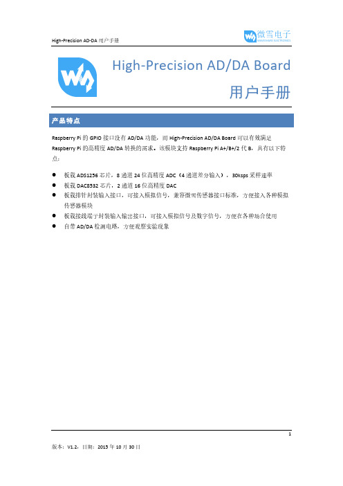
High-Precision AD/DA Board用户手册Raspberry Pi的GPIO接口没有AD/DA功能,而High-Precision AD/DA Board可以有效满足Raspberry Pi的高精度AD/DA转换的需求。
该模块支持Raspberry Pi A+/B+/2代B,具有以下特点:●板载ADS1256芯片,8通道24位高精度ADC(4通道差分输入),30ksps采样速率●板载DAC8532芯片,2通道16位高精度DAC●板载排针封装输入接口,可接入模拟信号,兼容微雪传感器接口标准,方便接入各种模拟传感器模块●板载接线端子封装输入输出接口,可接入模拟信号及数字信号,方便在各种场合使用●自带AD/DA检测电路,方便观察实验现象12板载资源[ 扩展接口]1.Raspberry Pi GPIO接口方便接入树莓派2.AD/DA输入输出接口(接线端子)方便在各种场合使用3.AD输入接口(排针)方便接入各种传感器模块(兼容微雪传感器接口标准)[ 器件介绍]4.7.68M晶振5.LM285-2.5提供ADC芯片工作基准电压6.光敏电阻7.LED输出指示灯8.10K电位器9.DAC853216位高精度DAC,2通道输出10.PWR LED电源指示灯11.ADS125624位高精度ADC,8通道(4通道差分输入)[ 跳线设置]12.ADC测试跳线13.DAC测试跳线14.电源配置跳线15.ADC参考地设置AD单端输入时,AINCOM为参考端,可接地或外部参考电平符号说明1)AD/DA输入输出接口(接线端子)(标号2)AD0-AD7:AD输入端AGND:模拟地GND:数字地VCC:工作电压(可通过电源配置跳线控制电压输出3.3V或者5V)DA0-DA1:DA输出端2)AD:AD输入接口(标号3)AD0-AD7:ADS1256模拟输入接口D0-D3:ADS1256的GPIO管脚(参考ADS1256数据手册)P22-P25:树莓派GPIO管脚AGND:模拟地3)LDR:光敏电阻(标号6)通过连接AD1和LDR之间的跳线,MCU可从AD1采集到该光敏电阻的输出电压。
AD9116中文资料

元器件交易网
AD9114/AD9115/AD9116/AD9117
TABLE OF CONTENTS
Features .............................................................................................. 1 Applications....................................................................................... 1 General Description ......................................................................... 1 Product Highlights ........................................................................... 1 Revision History ............................................................................... 2 Functional Block Diagram .............................................................. 3 Specifications..................................................................................... 4
2. CMOS Clock Input. High speed, single-ended CMOS clock input supports 125 MSPS conversion rate.
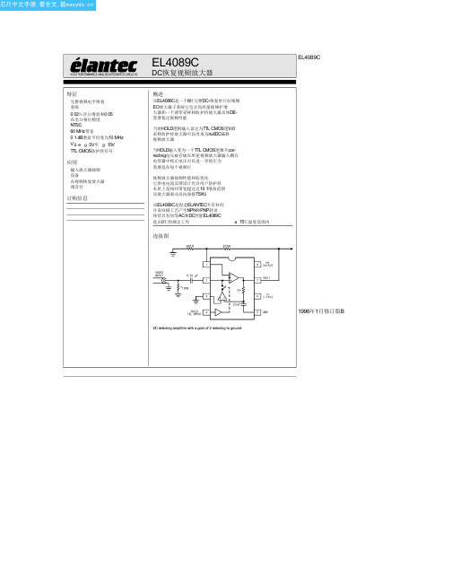
EL4089CS中文资料(Elantec Semiconductor)中文数据手册「EasyDatasheet - 矽搜」
a 25 C
12
25
II
mV
Ib a
IN a Input BiasCurrent
a 25 C
1
5
II
mA
Ib b
IN b Input BiasCurrent
a 25 C
18
150
II
mA
R
Transimpedance (Note 1)
a 25 C
180
800
II
kX
R
IN b Resistance
a 25 C
All parametershaving Min Max specificationsare guaranteed The Test Level column indicatesthe specific device testing actually
performed during production and Quality inspection Elantec performsmost electrical testsusing modern high-speed automatic test
20
V
X
CMRR
Common Mode Rejection Ratio (Note 2)
a 25 C
44
60
II
dB
V
Output Voltage Swing
a 25 C
12
13
II
V
I Restore Section
Short Circuit Current (IN a Only Driven to 0 5V)
3
TD is3 2in TD is3 2in
AD9851中文数据手册

AD9851中文数据手册By Hi_Cracker @whuCMOS180 MHzDDS / DAC合成器---------- AD9851FEATURES180 MHz的时钟速率可选6*参考时钟片上高性能10位DAC和高速滞回比较器无杂散动态范围(SFDR > 43分贝@70 MHzAout。
32bit 频率控制字便捷的编辑控制接口:并行或串行异步加载格式5位相位调制和偏置功能比较器抖动<80 ps的P-P在20兆赫2.7 V至5.25 V单电源供电低功耗:555毫瓦@180 MHz 掉电功能:4 mW@2.7 V 超小28引脚SSOP封装应用:频率/相位灵活可变的正弦波合成数字时钟恢复和锁定电路通信领域数控ADC编码发生器通信领域中灵活地本地振荡器正交振荡器CW,AM,FM,FSK MSK调制发射机GENERAL DESCRIPTIONAD9851是一个高度集成的器件,采用先进的DDS技术,结合内部高速,高性能D / A转换器,比较器,实现了一个数字可编程频率合成器和时钟发生器的功能。
引入一个精确的时钟源,AD9851可以产生一个稳定的,频率和相位可编程的正弦波。
此正弦波可以直接用作频率源或在内部转化为方波,然后作为灵活的时钟发生器使用。
AD9851的创新型高速DDS内核可以接受一个32位频率控制字,从而可以产生一个最大180 MHz的输出时钟,其分辨率约0.04Hz。
AD9851包含一个独特的6 * REFCLK乘法器电路,不再需要一个高速参考振荡器。
6 * REFCLK乘法器对SFDR和相位噪声的影响微乎其微。
AD9851提供分辨率为5位的相位调节,使其输出波形的相位的增量为11.25 °。
AD9851内部包含一个高速比较器,该比较器可以被配置为接受(外部)DAC的滤波输出,从而产生一个低抖动的输出脉冲。
频率的调谐,控制字以及相位调制字是通过并行或串行加载模式异步加载到AD9851中的。
莫萨 EDS-405A 408A-PN 系列 5 和 8 端口 managed Ethernet 交

EDS-405A/408A-PN SeriesIntroductionThe EDS-405A/408A-PN are 5 and 8-port managed Ethernet switches with PROFINET enabled. With embedded PROFINET, the PN switches can be easily integrated into the Simatic Step 7 engineering tool. It is more convenient for automation engineers to configure through Step 7 and monitor with automation HMIs. The EDS-405A/408A-PN• Command Line Interface (CLI) for quickly configuring major managed functions• IPv6 Ready logo awarded (IPv6 Logo Committee certified)• DHCP Option 82 for IP address assignment with different policies • Support EtherNet/IP and Modbus/TCP protocols for device management and monitoring• PROFINET v2 conformance class B, GSD (General StationDescription) v2, and SIMATIC STEP 7 device icons are available • Turbo Ring and Turbo Chain (recovery time < 20 ms @ 250 switches), and RSTP/STP for network redundancySpecificationsswitches with fast booting, Turbo Ring and Turbo Chain fast-recovery technology, can optimize PROFINET network performance. Moxa’s PROFINET switches also support a variety of useful management functions, such as IGMP snooping, IEEE 802.1Q VLAN, QoS, port mirroring, SNMP , bandwidth management, and warning by email or relay.• IGMP snooping and GMRP for filtering multicast traffic• Port-based VLAN, IEEE 802.1Q VLAN, and GVRP to ease network planning• QoS (IEEE 802.1p and TOS/DiffServ) to increase determinism • RMON for efficient network monitoring and proactive capability • SNMPv1/v2c/v3 for different levels of network management security• Bandwidth management to prevent unpredictable network status • Port mirroring for online debuggingFeatures and BenefitsTechnologyStandards:IEEE 802.3 for 10BaseTIEEE 802.3u for 100BaseT(X) IEEE 802.3x for Flow ControlIEEE 802.1D-2004 for Spanning Tree Protocol IEEE 802.1w for Rapid STP IEEE 802.1p for Class of Service IEEE 802.1Q for VLAN TaggingProtocols: IGMPv1/v2, GMRP, GVRP, SNMPv1/v2c/v3, DHCP Server/Client, TFTP, SNTP, SMTP, RARP, RMON, HTTP, Telnet, Syslog, DHCP Option 66/67/82, BootP, LLDP, PROFINET, EtherNet/IP, Modbus/TCP, IPv6, NTP Server/ClientMIB: MIB-II, Ethernet-Like MIB, P-BRIDGE MIB, Bridge MIB, RSTP MIB, RMON MIB Group 1, 2, 3, 9Flow Control: IEEE 802.3x flow control, back pressure flow controlSwitch PropertiesMAC Table Size: 2 K (EDS-405A-PN), 8 K (EDS-408A-PN)Packet Buffer Size: 1 MbitInterfaceRJ45 Ports: 10/100BaseT(X) auto negotiation speed, Full/Half duplex mode, and auto MDI/MDI-X connection Console Port: RS-232 (RJ45 connector)DIP Switches: Turbo Ring, Master, Coupler, ReserveLED Indicators: PWR1, PWR2, FAULT, MSTR/HEAD, CPLR/TAIL, 10/100MAlarm Contact: 1 relay output with current carrying capacity of 1 A @ 24 VDCPower RequirementsInput Voltage: 24 VDC (12 to 45 VDC), redundant dual inputs Input Current:EDS-405A-PN: 0.24 A @ 24 V EDS-408A-PN: 0.26 A @ 24 VOverload Current Protection: PresentConnection: 1 removable 6-contact terminal block Reverse Polarity Protection: PresentPhysical CharacteristicsHousing: Metal, IP30 protectionDimensions: 53.6 x 135 x 105 mm (2.11 x 5.31 x 4.13 in)Packing Size: 19.2 x 16.8 x 9.3 cm Weight: 650 g Packing Weight:EDS-405A-PN series: 1140 g EDS-408A-PN series: 1220 gInstallation: DIN-rail mounting, wall mounting (with optional kit)Standard Models: 0 to 60°C (32 to 140°F)Wide Temp. Models: -40 to 75°C (-40 to 167°F)Storage Temperature: -40 to 85°C (-40 to 185°F)Ambient Relative Humidity: 5 to 95% (non-condensing)Standards and CertificationsSafety: UL 508, UL 60950-1, CSA C22.2 No. 60950-1, EN 60950-1**Hazardous Location: UL/cUL Class I Division 2 Groups A/B/C/D, ATEX Zone 2 Ex nC IICEMI: FCC Part 15 Subpart B Class A, EN 55022 Class A EMS:EN 61000-4-2 (ESD) Level 3, EN 61000-4-3 (RS) Level 3, EN 61000-4-4 (EFT) Level 3, EN 61000-4-5 (Surge) Level 3, EN 61000-4-6 (CS) Level 3, EN 61000-4-8Marine: DNV, GLTraffic Control: NEMA TS2Freefall: IEC 60068-2-32Vibration: IEC 60068-2-6* EDS-405A/408A-PN ** EDS-408A-PN onlyNote: Please check Moxa’s website for the most up-to-date certification status.MTBF (mean time between failures)Time:EDS-405A-PN Series: 392,000 hrs EDS-408A-PN Series: 363,000 hrs Database: Telcordia (Bellcore), GBWarrantyWarranty Period: 5 yearsDetails: See /warrantyPackage Checklist• EDS-405A-PN or EDS-408A-PN switch • RJ45 to DB9 console port cable • Protective caps for unused ports • Documentation and software CD • Hardware installation guide (printed)•Warranty cardOptional Accessories (can be purchased separately)MXview: Moxa industrial network management software with 50, 100, 250, 500, 1000, or 2000 nodes EDS-SNMP OPC Server Pro: OPC server software that works with all SNMP devicesABC-01: Configuration backup and restoration tool for managed Ethernet switches, 0 to 60°C operating temperatureDR-4524/75-24/120-24: 45/75/120 W DIN-rail 24 VDC power suppliesMDR-40-24/60-24: 40/60 W DIN-rail 24 VDC power supplies, -20 to 70°C operating temperature WK-46: Wall mounting kitRK-4U: 4U-high 19” rack mounting kit。
AD590中文资料全

AD590中文资料特点:线性电流传感器:1uA/K范围:55°C-+150°C陶瓷传感器探头兼容包终端装置:电压/电流激光微调到±0.5°C校准精度(AD590M)良好的线性:±0.3°C覆盖全量程(AD590M)供电电压范围:+4V-+30V独立传感器低成本产品说明:AD590是一个将输出电流比例转换成绝对温度的二终端集成电路温度变换装置。
为电源电压在+4V和+30V之间设备作为一个高阻抗、恒定电流为1uA/K的装置。
芯片的薄膜电阻器的激光微调装置被用于将设备微调至在298.2K(+25°C)时输出298.2uA。
AD590应该被应用于任意温度感应在+150°C之下,在这个温度下,传统的温度感应装置都可以使用。
一个整体集成电路的固有低成本与支持电路牌子的排除结合了AD590一个有吸引力的选择为许多温度测量情况。
线性化电路、精确度电压放大器、抵抗测量的电路和冷接点报偿不必要在申请AD590。
除温度测量之外,应用包括温度分离组分的报偿或更正,偏心比例与绝对温度,流速测量,流体的平实侦查和测速。
AD590可以在芯片的形式封装,在保护的环境下,它适用于混合电路和快速温度测量。
AD590在遥感应用方面特别好用。
由于它的高阻抗电流输出,设备对长线性的电压下降不敏感。
任何良好的绝缘绞的一双都能很好的从接收CMOS多路复用器或者切换逻辑门输出的电源电压。
产品特点:①AD590是一个要求只有一个直流电源电压(+4V to+30V)的校准的双终端温度传感器。
昂贵的发射器,滤波器,导致线性补偿和线性化电路是应用设备所不必要的。
②国家最先进的晶圆级激光修剪的广泛最终测试确保了AD590的单元的易于更换。
③是电流而不是电压的输出导致了优先接口的排斥反应。
此外,电压需求低(1.5mWs@ 5V@+25°C.)。
这些功能使得AD590易于应用于远程传感器。
AD408M182VBB-5中文资料

ASCEND Semiconductor 4Mx4 EDO Data sheetDescriptionThe device CMOS Dynamic RAM organized as 4,194,304 words x 4 bits with extended data out access mode. It is fabricated with an advanced submicron CMOS technology and designed to operate from a single 3.3V oniy power supply. Low voltage operation is more suitable to be used on battery backup, portable elec-tronic application. lt is packaged in JEDEC standard 26/24-pin plastic SOJ or TSOP(II).Features• Single 3.3V(%) only power supply • High speed t RAC acess time: 50/60ns • Low power dissipation- Active mode : 432/396 mW (Mas) - Standby mode: 0.54 mW (Mas)• Extended - data - out(EDO) page mode access • I/O level: CMOS level (Vcc = 3.3V)• 2048 refresh cycle in 32 ms(Std.) or 128 ms(S-version)• 4 refresh modesh: - RAS only refresh- CAS - before - RAS refresh - Hidden refresh - Self-refresh(S-version)10±Pin Name FunctionA0-A10Address inputs- Row address - Column address - Refresh address DQ1~DQ4Data-in / data-out RAS Row address strobe CAS Column address strobe WE Write enable OE Output enable Vcc Power (+ 3.3V)VssGroundVCC 1DQ12DQ23DQ34DQ45VCC6891011 NC 12 WE 13A0 A117 A218 A319VSS RAS CAS OE A8A7A6A5A4VSSAD404M42VSPin Description Pin Configuration21222324 2526151416 A1026/24-PIN 300mil Plastic SOJA9VCC 1DQ12DQ23DQ34DQ45VCC6891011 NC 12 WE 13A0 A117 A218 A319VSS RAS CAS OE A8A7 A6A5 A4VSSAD404M42VT212223242526151416 A1026/24-PIN 300mil Plastic TSOP (ll)A9A0-A10A0-A10A0-A10WECASNO. 2 CLOCK GENERATORCOLUMN ADDRESS BUFFERS (11)REFRESH CONTROLLERREFRESH COUNTERBUFFERS (11)ADDRESS ROW NO. 1 CLOCK GENERATORA0RASA1A2A3A4A5A6A7A8CONTROLLOGICDATA-IN BUFFERDATA-OUT BUFFEROEDQ1.DQ4.COLUMN DECODER2048SENSE AMPLIFIERSI/O GATING2048x42048x2048x4MEMORY ARRAY2048R O W D E C O D E RVcc VssBlock DiagramA9A10TRUTH TABLENotes: 1. EARLY WRITE only.FUNCTIONRASCAS WE OE ADDRESSESDQ SNotesROW COL STANDBY H X X X X High-Z READL L H L ROW COL Data-Out WRITE: (EARLY WRITE )L L L X ROW COL Data-lnREAD WRITE L L ROW COL Data-Out,Data-ln EDO-PAGE-MODE READ1st Cycle L H L ROW COL Data-Out 2nd CycleL H L n/a COL Data-Out EDO-PAGE MODE WRITE1st CycleL L X ROW COL Data-In 2nd Cycle L L Xn/a COL Data-InEDO-PAGE-MODEREAD-WRITE 1st Cycle L ROW COL Data-Out, Data-In 2nd Cycle L n/a COL Data-Out, Data-In HIDDEN REFRESHREAD L H L ROW COL Data-Out WRITEL L X ROW COL Data-In 1RAS-ONLY REFRESH L H X X ROW n/a High-Z CBR REFRESHLHXXXHigh-ZH X →H L →L H →H L →H L →H L →H L →H L →H L →L H →H L →H L →L H→L H L →→L H L→→H L→Absolute Maximum RatingsRecommended DC Operating ConditionsCapacitanceTa = 25°C, V CC = 3.3V%, f = 1MHz Note: 1. Capacitance measured with effective capacitance measuring method. 2. RAS, CAS = V IH to disable Dout.ParameterSymbol Value Unit Voltage on any pin relative to Vss V T -0.5 to + 4.6V Supply voltage relative to Vss V CC -0.5 to + 4.6V Short circuit output current I OUT 50mA Power dissipation P D 1.0WOperating temperature T OPT 0 to + 70°C Storage temperatureT STG-55 to + 125°CParameter/Condition Symbol3.3 Volt VersionUnitMinTyp MaxSupply VoltageV CC 3.0 3.33.6V Input High Voltage, all inputs V IH 2.0-V CC + 0.3V Input Low Voltage, all inputsV IL-0.3-0.8VParameterSymbol Typ Max Unit Note Input capacitance (Address)C I1 -5pF 1Input capacitance (RAS, CAS, OE, WE)C I2-7pF 1Output capacitance(Data-in, Data-out)C I/O-7pF1, 210±DC Characteristics :(T a = 0 to 70°C, V CC = + 3.3V%, V SS = 0V)Parameter Symbol Test Conditions AD404M42V Unit Notes-5-6Min Max Min MaxOperating current I CC1RAS cyclingCAS, cyclingt RC = min-120-110mA1, 2Standby Current LowpowerS-versionI CC2LVTTL interfaceRAS, CAS = V IHDout = High-Z-0.5-0.5mACMOS interfaceRAS, -0.2VDout = High-Z-0.15-0.15mAStandardpowerversionLVTTL interfaceRAS, CAS = V IHDout = High-Z-2-2mACMOS interfaceRAS,-0.2VDout = High-Z-0.5-0.5mARAS- only refresh current I CC3RAS cycling, CAS = V IHt RC = min-120-110mA1, 2 EDO page mode current I CC4t PC = min-90-80mA1, 3CAS- before- RAS refresh current I CC5t RC = minRAS, CAS cycling-120-110mA1, 2Self- refresh current (S-Version)I CC8 - 550 - 55010±CAS V CC≥CAS V CC≥t RASS100µs≥µADC Characteristics :(T a = 0 to 70°C , V CC = +3.3V %, V SS = 0V)Notes:1. I CC is specified as an average current. It depends on output loading condition and cycle rate when the device is selected. I CC max is specified at the output open condition.2. Address can be changed once or less while RAS = V IL .3. For I CC4, address can be changed once or less within one EDO page mode cycle time.Parameter Symbol Test Conditions AD404M42VUnitNotes-5-6Min MaxMin MaxInput leakage current I LI + 0.3V -55-55Output leakage current I LO + 0.3V Dout = Disable -55-55Output high Voltage V OH I OH = -2mA 2.4- 2.4-V Output low voltage V OLI OL = +2mA-0.4-0.4V10±0V Vin V CC ≤≤µA 0V Vout V CC ≤≤µAAC Characteristics(T a = 0 to + 70°C , V cc = 3.3V %, V ss = 0V) *1, *2, *3, *4Test conditions• Output load: one TTL Load and 100pF (V CC = 3.3V %)• Input timing reference levels:V IH = 2.0V, V IL = 0.8V (V CC = 3.3V %)• Output timing reference levels:V OH = 2.0V, V OL = 0.8V10±10±10±Read, Write, Read- Modify- Write and Refresh Cycles (Common Parameters)ParameterSymbol AD404M42V UnitNotes-5-6Min MaxMin MaxRandom read or write cycle time t RC 84-104-ns RAS precharge timet RP 30-40-ns CAS precharge time in normal mode t CPN 10-10-ns RAS pulse width t RAS 50100006010000ns 5CAS pulse width t CAS 8100001010000ns 6Row address setup time t ASR 0-0-ns Row address hold time t RAH 8-10-ns Column address setup time t ASC 0-0-ns 7Column address hold time t CAH 8-10-ns RAS to CAS delay timet RCD 12371445ns 8RAS to column address delay time t RAD 10251230ns 9Column address to RAS lead time t RAL 25-30-ns RAS hold time t RSH 8-10-ns CAS hold timet CSH 38-40-ns CAS to RAS precharge time t CRP 5-5-ns 10OE to Din delay time t OED 12-15-ns Transition time (rise and fall)t T 150150ns 11Refresh periodt REF -32-32ms Refresh period (S- Version)t REF -128-128ms CAS to output in Low- Z t CLZ 0-0-ns CAS delay time from Din t DZC 0-0-ns OE delay time from Dint DZO-0-nsRead CycleWrite Cycle Parameter SymbolAD404M42V Unit Notes-5-6Min Max Min MaxAccess time from RAS t RAC-50-60ns12 Access time from CAS t CAC-14-15ns13, 14 Access time from column address t AA-25-30ns14, 15 Access time from OE t OEA-12-15nsRead command setup time t RCS0-0-ns7 Read command hold time to CAS t RCH0-0-ns10, 16 Read command hold time to RAS t RRH0-0-ns16 Output buffer turn-off time t OFF012015ns17 Output buffer turn-off time from OE t OEZ012015ns17Parameter SymbolAD404M42V Unit Notes -5-6Min Max Min MaxWrite command setup time t WCS0-0-ns7, 18 Write command hold time t WCH8-10-nsWrite command pulse width t WP8-10-nsWrite command to RAS lead time t RWL13-15-nsWrite command to CAS lead time t CWL8-10-nsData-in setup time t DS0-0-ns19 Data-in hold time t DH8-10-ns19 WE to Data-in delay t WED10-10-nsRead- Modify- Write CycleRefresh Cycle Parameter SymbolAD404M42V Unit Notes-5-6Min Max Min MaxRead-modify- write cycle time t RWC108-133-nsRAS to WE delay time t RWD64-77-ns18 CAS to WE dealy time t CWD26-32-ns18 Column address to WE delay time t AWD39-47-ns18 OE hold time from WE t OEH8-10-nsParameter SymbolAD404M42VUnit Notes -5-6Min Max Min MaxCAS setup time (CBR refresh) t CSR5-5-nsCAS hold time (CBR refresh)t CHR8-10-ns10 RAS precharge to CAS hold time t RPC5-5-ns7 RAS pulse width (self refresh)t RASS100-100-RAS precharge time (self refresh)t RPS90-110-nsCAS hold time (CBR self refresh)t CHS-50--50-nsWE setup time t WSR0-0-nsWE hold time t WHR10-10-nsµsEDO Page Mode CycleEDO Page Mode Read Modify Write CycleParameterSymbol AD404M42VUnit Notes-5-6Min MaxMin MaxEDO page mode cycle timet PC 20-25-ns EDO page mode CAS precharge time t CP 10-10-ns EDO page mode RAS pulse width t RASP 5010560105ns 20Access time from CAS precharge t CPA -30-35ns 10, 14RAS hold time from CAS precharge t CPRH 30-35-ns OE high hold time from CAS high t OEHC 5-5-ns OE high pulse widtht OEP 10-10-ns Data output hold time after CAS low t COH 5-5-ns Output disable delay from WEt WHZ 310310ns WE pulse width for output disable whenCAS hight WPZ7-7-nsParameterSymbol AD404M42V Unit Notes -5-6Min MaxMin MaxEDO page mode read- modify- write cycle CAS precharge to WE delay timet CPW 45-55-ns 10EDO page mode read- modify- write cycle timet PRWC56-68-nsNotes :1. AC measurements assume t T = 2ns.2. An initial pause of 100 is required after power up, and it followed by a minimum of eightinitialization cycles (RAS - only refresh cycle or CAS - before - RAS refresh cycle). If the internal refresh counter is used, a minimun of eight CAS - before - RAS refresh cycles are required.3. In delayed write or read-modify-write cycles, OE must disable output buffer prior to applying data to the device.4. All the V CC and V SS pins shall be supplied with the same voltages.5. t RAS (min) = t RWD (min)+t RWL (min)+t T in read-modify-write cycle.6. t CAS (min) = t CWD (min)+t CWL (min)+t T in read-modify-write cycle.7. t ASC (min), t RCS (min), t WCS (min), and t RPC are determined by the falling edge of CAS .8. t RCD (max) is specified as a reference point only, and t RAC (max) can be met with the t RCD (max) limit.Otherwise, t RAC is controlled exclusively by t CAC if t RCD is greater than the specified t RCD (max) limit. 9. t RAD (max) is specified as a reference point only, and t RAC (max) can be met with the t RAD (max) limit.Otherwise, t RAC is controlled exclusively by t AA if t RAD is greater than the specified t RAD (max) limit. 10. t CRP , t CHR , t RCH , t CPA and t CPW are determined by the rising edge of CAS .11. V IH (min) and V IL (max) are reference levels for measuring timing or input signals. Therefore, transitiontime is measured between V IH and V IL .12. Assumes that t RCD tRCD (max) and t RAD t RAD (max). If t RCD or t RAD is greater than the maximum recommended value shown in this table, t RAC exceeds the value shown. 13. Assumes that (max) and (max).14. Access time is determined by the maximum of t AA , t CAC , t CPA . 15. Assumes that (max) and (max). 16. Either t RCH or t RRH must be satisfied for a read cycle.17. t OFF (max) and t OEZ (max) define the time at which the output achieves the open circuit condition (highimpedance). t OFF is determined by the later rising edge of RAS or CAS.18. t WCS , t RWD , t CWD , and t AWD are not restrictive operating parameters. They are included in the datasheet as electrical characteristics only. If (min), the cycle is an early write cycle and the data out will remain open circuit (high impedance) throughout the entire cycle. If (min),(min), (min) and (min), the cycle is a read-modify-write and the data output will contain data read from the selected cell. If neither of the above sets of conditions is satisfied, the condition of the data output (at access time) is indeterminate.19. These parameters are referenced to CAS separately in an early write cycle and to WE edge in adelayed write or a read-modify-write cycle.20. t RASP defines RAS pulse width in EDO page mode cycles.µs ≤≤t RCD t RCD ≥t RADt RAD ≤t RCD t RCD ≤t RAD t RAD ≥t WCS t WCS ≥t RWD t RWD ≥t CWDt CWD ≥t AWD t AWD ≥t CPW t CPW≥Timing Waveforms• Read Cyclet RC t RASt RPtCRPtCPNtRRHtRCHt OEZ t OFF tOEA tCACt AAtRACt CLZD OUTtRCS t ASR tRAH tASC tCAH tRAD t RALtCAStRSH tRCDt TtCSHRASCASADDRESSWEDQ1~DQ4Note : = don’t care OEt OFFRowColumn= Invalid Dout•Early Write CycletRC t RASt RPt WCHt DSt DHt WCS t RALtCAStRSH tRCDt TtCSHRASCASWEDQ1~DQ4tCRPtASRtRAH tASCtCAH ADDRESSColumnRowtCPND INtRADt RAL• Delayed Write CycletRC t RASt RPt RWL t RCSt CAStRSH tRCDt TtCSHRASCAStASR tRAH tCAHADDRESSColumnRow tASC D INDQ1~DQ4WEtCRPtCPNt DHt DSt OEHt OEDOEt DSOPENt WPt CWL• Read - Modify - Write CycletRWC t RASt RPtRWDt WPtRADtRWL tCAStCWL tRCDt TtCPNRASCASWEtCRP t ASRtRAHtASCtCAHADDRESS Column RowDQ1~DQ4t DHt DSOEtRCStAWD tCWD D INt OEDt OEHt OEZt OEA t CAC t RACt AADQ1~DQ4D OUTOPENtDZCtDZO• EDO Page Mode Read CycletRASPtCPRHt RCStCAStRSH tRCDt OEAtCSHRASCAStASRtRAHtCAHADDRESStCASWEtCRPt CPOEDQ1~DQ4OPENtOEPD OUT 1t PCt CPtCAStCPNtCRPtRADtCAHtASCt ASCtCAHt ASCt RAL Row Column 1t OEAt OEHCtRRH tRCHt RACt AAt AAt AA t CPA t CPA t OEZt OFFt OFFt CACt OEZt CAC t CACt COHD OUT NWE OE Column 2Column N Rowt RPD OUT 2• EDO Page Mode Early Write CycletRASPtRPt WCSt CAStRSH tRCDRASCAStASRtRAHtCAHADDRESStCASWEt CPDQ1~DQ4t PCt CPt CAStCPNtCRP tCAH tASCtASC tCAH tASC Row Column 1t DS WE Column 2Column Nt WCH t WCS t WCH t WCS t WCHt DH t DS t DH t DS t DHD IN 1D IN 2D IN Nt TtCSH• EDO Page Mode Read-Early-Write Cyclet RASPtCPRHt RCStCAStRSH tRCDt OEAtCSHRASCAStASRtRAHtCAHADDRESStCASWEtCRPt CPOEDQ1~DQ4OPENtWEDt PCt CPtCAStCPNtCRPtRADtRAHtASCt ASCtCAHt ASCt RAL Row Column 1tWCStRCHt RACt AAt AAt CPA t DHt WHZt CACt CACt COHWE OE Column 2Column N Rowt RPt CAL tWCHDataDoutput 2Data Input NDataDoutput 1t DStCSH• EDO Page Mode Read-Modify-Write Cyclet RASPt CPRHt RCStCASt WP RASCASt ASRtRAHtCAHADDRESSt CASWEtRCDCPDQ1~DQ4tPRWCt CPtCAStCRPtRADtCAHtASCt ASCtCAH tASC Row Column 1tRWLtRCSt OEDt DZOt CAC WE OEt RPt RAL D OUT 2D OUT ND OUT 1tTt Column NColumn 2Column 1tRWD tAWD tCWDtCWLtRCStCWDtAWD tCPW tCWL tCPW tAWD tCWDtCWL t OEDt OEDt OEHt OEHt OEHt CAC t CAC t OEA t AAt RACt OEZt OEAt AA t CPAt OEZt OEAt AA t CPAt OEZ t DSt DHt WP t DSt DHt WP t DSt DHOPENOPENOPEN D IN 1D IN ND IN 2DQ1~DQ4t DZCt DZOt DZCt DZCt DZO• Read Cycle with WE Controlled Disablet WPZt RCStCAStRCDt TtCSHRASCASt ASRtRAHtCAHADDRESSColumnRow tASCD DQ1~DQ4WEt OEZt DSt WHZOEt RCH t OEA t CACt AAt RACt CLZOUTtRADRASADDRESSt RC t CRPt ASRt RAHt Tt RPCROWt OFFCAS t RASt RPOPENt CRPDQ1~DQ4RASt CSRt WSRt RPt T t RPCt OFFCAS t RASt RPOPENt CRPDQ1~DQ4t RPCt CHRt RASt RPt RCt RCt CHRt CSRt WHRt WSRt WHRWECAS-Before-RAS Refresh CycleRASWEt RPCt OFFt CSRt CHSt WSRCASt RASS t RPSOPENDQ1~DQ4t WHRHigh lmpedance• Hidden Refresh Cyclet RPt RASRASt RCDt CRPADDRESSWEt CHRt CASt RSHt RAHt ASRt ASCt CAHt RAL ROW t RCHt OEZCASDQ1~DQ4t Tt RCSD t RASt RASt RPt RPt RC t RCt RCt RADt RRHt OFF t OFFt OEA t CACt AAt RACCOlumnOUTOE(READ)(REFRESH)(REFRESH)Ordering informationAD404M42VSA-5• AD• Ascend Memory Product • 40 • Device Type• 4M4 • Density and Organization • 2• Refresh Rate, 2: 2K Refresh • V• T: 5V, V: 3.3V• S • Package Type (S : SOJ, T : TSOP II)• A• Version• 5• Speed (5: 50 ns, 6: 60 ns)Part Number Access time PackageAD404M42VSA-5AD404M42VSA-6AD404M42VTA-5AD404M42VTA-650 ns 60 ns 50 ns 60 ns300mil 26/24-Pin Plastic SOJTSOP IIPackaging information • 300 mil, 26/24-Pin Plastic SOJ• 300 mil, 26/24-Pin TSOP II。
- 1、下载文档前请自行甄别文档内容的完整性,平台不提供额外的编辑、内容补充、找答案等附加服务。
- 2、"仅部分预览"的文档,不可在线预览部分如存在完整性等问题,可反馈申请退款(可完整预览的文档不适用该条件!)。
- 3、如文档侵犯您的权益,请联系客服反馈,我们会尽快为您处理(人工客服工作时间:9:00-18:30)。
ASCEND Semiconductor 4Mx4 EDO Data sheetDescriptionThe device CMOS Dynamic RAM organized as 4,194,304 words x 4 bits with extended data out access mode. It is fabricated with an advanced submicron CMOS technology and designed to operate from a single 3.3V oniy power supply. Low voltage operation is more suitable to be used on battery backup, portable elec-tronic application. lt is packaged in JEDEC standard 26/24-pin plastic SOJ or TSOP(II).Features• Single 3.3V(%) only power supply • High speed t RAC acess time: 50/60ns • Low power dissipation- Active mode : 432/396 mW (Mas) - Standby mode: 0.54 mW (Mas)• Extended - data - out(EDO) page mode access • I/O level: CMOS level (Vcc = 3.3V)• 2048 refresh cycle in 32 ms(Std.) or 128 ms(S-version)• 4 refresh modesh: - RAS only refresh- CAS - before - RAS refresh - Hidden refresh - Self-refresh(S-version)10±Pin Name FunctionA0-A10Address inputs- Row address - Column address - Refresh address DQ1~DQ4Data-in / data-out RAS Row address strobe CAS Column address strobe WE Write enable OE Output enable Vcc Power (+ 3.3V)VssGroundVCC 1DQ12DQ23DQ34DQ45VCC6891011 NC 12 WE 13A0 A117 A218 A319VSS RAS CAS OE A8A7A6A5A4VSSAD404M42VSPin Description Pin Configuration21222324 2526151416 A1026/24-PIN 300mil Plastic SOJA9VCC 1DQ12DQ23DQ34DQ45VCC6891011 NC 12 WE 13A0 A117 A218 A319VSS RAS CAS OE A8A7 A6A5 A4VSSAD404M42VT212223242526151416 A1026/24-PIN 300mil Plastic TSOP (ll)A9A0-A10A0-A10A0-A10WECASNO. 2 CLOCK GENERATORCOLUMN ADDRESS BUFFERS (11)REFRESH CONTROLLERREFRESH COUNTERBUFFERS (11)ADDRESS ROW NO. 1 CLOCK GENERATORA0RASA1A2A3A4A5A6A7A8CONTROLLOGICDATA-IN BUFFERDATA-OUT BUFFEROEDQ1.DQ4.COLUMN DECODER2048SENSE AMPLIFIERSI/O GATING2048x42048x2048x4MEMORY ARRAY2048R O W D E C O D E RVcc VssBlock DiagramA9A10TRUTH TABLENotes: 1. EARLY WRITE only.FUNCTIONRASCAS WE OE ADDRESSESDQ SNotesROW COL STANDBY H X X X X High-Z READL L H L ROW COL Data-Out WRITE: (EARLY WRITE )L L L X ROW COL Data-lnREAD WRITE L L ROW COL Data-Out,Data-ln EDO-PAGE-MODE READ1st Cycle L H L ROW COL Data-Out 2nd CycleL H L n/a COL Data-Out EDO-PAGE MODE WRITE1st CycleL L X ROW COL Data-In 2nd Cycle L L Xn/a COL Data-InEDO-PAGE-MODEREAD-WRITE 1st Cycle L ROW COL Data-Out, Data-In 2nd Cycle L n/a COL Data-Out, Data-In HIDDEN REFRESHREAD L H L ROW COL Data-Out WRITEL L X ROW COL Data-In 1RAS-ONLY REFRESH L H X X ROW n/a High-Z CBR REFRESHLHXXXHigh-ZH X →H L →L H →H L →H L →H L →H L →H L →H L →L H →H L →H L →L H→L H L →→L H L→→H L→Absolute Maximum RatingsRecommended DC Operating ConditionsCapacitanceTa = 25°C, V CC = 3.3V%, f = 1MHz Note: 1. Capacitance measured with effective capacitance measuring method. 2. RAS, CAS = V IH to disable Dout.ParameterSymbol Value Unit Voltage on any pin relative to Vss V T -0.5 to + 4.6V Supply voltage relative to Vss V CC -0.5 to + 4.6V Short circuit output current I OUT 50mA Power dissipation P D 1.0WOperating temperature T OPT 0 to + 70°C Storage temperatureT STG-55 to + 125°CParameter/Condition Symbol3.3 Volt VersionUnitMinTyp MaxSupply VoltageV CC 3.0 3.33.6V Input High Voltage, all inputs V IH 2.0-V CC + 0.3V Input Low Voltage, all inputsV IL-0.3-0.8VParameterSymbol Typ Max Unit Note Input capacitance (Address)C I1 -5pF 1Input capacitance (RAS, CAS, OE, WE)C I2-7pF 1Output capacitance(Data-in, Data-out)C I/O-7pF1, 210±DC Characteristics :(T a = 0 to 70°C, V CC = + 3.3V%, V SS = 0V)Parameter Symbol Test Conditions AD404M42V Unit Notes-5-6Min Max Min MaxOperating current I CC1RAS cyclingCAS, cyclingt RC = min-120-110mA1, 2Standby Current LowpowerS-versionI CC2LVTTL interfaceRAS, CAS = V IHDout = High-Z-0.5-0.5mACMOS interfaceRAS, -0.2VDout = High-Z-0.15-0.15mAStandardpowerversionLVTTL interfaceRAS, CAS = V IHDout = High-Z-2-2mACMOS interfaceRAS,-0.2VDout = High-Z-0.5-0.5mARAS- only refresh current I CC3RAS cycling, CAS = V IHt RC = min-120-110mA1, 2 EDO page mode current I CC4t PC = min-90-80mA1, 3CAS- before- RAS refresh current I CC5t RC = minRAS, CAS cycling-120-110mA1, 2Self- refresh current (S-Version)I CC8 - 550 - 55010±CAS V CC≥CAS V CC≥t RASS100µs≥µADC Characteristics :(T a = 0 to 70°C , V CC = +3.3V %, V SS = 0V)Notes:1. I CC is specified as an average current. It depends on output loading condition and cycle rate when the device is selected. I CC max is specified at the output open condition.2. Address can be changed once or less while RAS = V IL .3. For I CC4, address can be changed once or less within one EDO page mode cycle time.Parameter Symbol Test Conditions AD404M42VUnitNotes-5-6Min MaxMin MaxInput leakage current I LI + 0.3V -55-55Output leakage current I LO + 0.3V Dout = Disable -55-55Output high Voltage V OH I OH = -2mA 2.4- 2.4-V Output low voltage V OLI OL = +2mA-0.4-0.4V10±0V Vin V CC ≤≤µA 0V Vout V CC ≤≤µAAC Characteristics(T a = 0 to + 70°C , V cc = 3.3V %, V ss = 0V) *1, *2, *3, *4Test conditions• Output load: one TTL Load and 100pF (V CC = 3.3V %)• Input timing reference levels:V IH = 2.0V, V IL = 0.8V (V CC = 3.3V %)• Output timing reference levels:V OH = 2.0V, V OL = 0.8V10±10±10±Read, Write, Read- Modify- Write and Refresh Cycles (Common Parameters)ParameterSymbol AD404M42V UnitNotes-5-6Min MaxMin MaxRandom read or write cycle time t RC 84-104-ns RAS precharge timet RP 30-40-ns CAS precharge time in normal mode t CPN 10-10-ns RAS pulse width t RAS 50100006010000ns 5CAS pulse width t CAS 8100001010000ns 6Row address setup time t ASR 0-0-ns Row address hold time t RAH 8-10-ns Column address setup time t ASC 0-0-ns 7Column address hold time t CAH 8-10-ns RAS to CAS delay timet RCD 12371445ns 8RAS to column address delay time t RAD 10251230ns 9Column address to RAS lead time t RAL 25-30-ns RAS hold time t RSH 8-10-ns CAS hold timet CSH 38-40-ns CAS to RAS precharge time t CRP 5-5-ns 10OE to Din delay time t OED 12-15-ns Transition time (rise and fall)t T 150150ns 11Refresh periodt REF -32-32ms Refresh period (S- Version)t REF -128-128ms CAS to output in Low- Z t CLZ 0-0-ns CAS delay time from Din t DZC 0-0-ns OE delay time from Dint DZO-0-nsRead CycleWrite Cycle Parameter SymbolAD404M42V Unit Notes-5-6Min Max Min MaxAccess time from RAS t RAC-50-60ns12 Access time from CAS t CAC-14-15ns13, 14 Access time from column address t AA-25-30ns14, 15 Access time from OE t OEA-12-15nsRead command setup time t RCS0-0-ns7 Read command hold time to CAS t RCH0-0-ns10, 16 Read command hold time to RAS t RRH0-0-ns16 Output buffer turn-off time t OFF012015ns17 Output buffer turn-off time from OE t OEZ012015ns17Parameter SymbolAD404M42V Unit Notes -5-6Min Max Min MaxWrite command setup time t WCS0-0-ns7, 18 Write command hold time t WCH8-10-nsWrite command pulse width t WP8-10-nsWrite command to RAS lead time t RWL13-15-nsWrite command to CAS lead time t CWL8-10-nsData-in setup time t DS0-0-ns19 Data-in hold time t DH8-10-ns19 WE to Data-in delay t WED10-10-nsRead- Modify- Write CycleRefresh Cycle Parameter SymbolAD404M42V Unit Notes-5-6Min Max Min MaxRead-modify- write cycle time t RWC108-133-nsRAS to WE delay time t RWD64-77-ns18 CAS to WE dealy time t CWD26-32-ns18 Column address to WE delay time t AWD39-47-ns18 OE hold time from WE t OEH8-10-nsParameter SymbolAD404M42VUnit Notes -5-6Min Max Min MaxCAS setup time (CBR refresh) t CSR5-5-nsCAS hold time (CBR refresh)t CHR8-10-ns10 RAS precharge to CAS hold time t RPC5-5-ns7 RAS pulse width (self refresh)t RASS100-100-RAS precharge time (self refresh)t RPS90-110-nsCAS hold time (CBR self refresh)t CHS-50--50-nsWE setup time t WSR0-0-nsWE hold time t WHR10-10-nsµsEDO Page Mode CycleEDO Page Mode Read Modify Write CycleParameterSymbol AD404M42VUnit Notes-5-6Min MaxMin MaxEDO page mode cycle timet PC 20-25-ns EDO page mode CAS precharge time t CP 10-10-ns EDO page mode RAS pulse width t RASP 5010560105ns 20Access time from CAS precharge t CPA -30-35ns 10, 14RAS hold time from CAS precharge t CPRH 30-35-ns OE high hold time from CAS high t OEHC 5-5-ns OE high pulse widtht OEP 10-10-ns Data output hold time after CAS low t COH 5-5-ns Output disable delay from WEt WHZ 310310ns WE pulse width for output disable whenCAS hight WPZ7-7-nsParameterSymbol AD404M42V Unit Notes -5-6Min MaxMin MaxEDO page mode read- modify- write cycle CAS precharge to WE delay timet CPW 45-55-ns 10EDO page mode read- modify- write cycle timet PRWC56-68-nsNotes :1. AC measurements assume t T = 2ns.2. An initial pause of 100 is required after power up, and it followed by a minimum of eightinitialization cycles (RAS - only refresh cycle or CAS - before - RAS refresh cycle). If the internal refresh counter is used, a minimun of eight CAS - before - RAS refresh cycles are required.3. In delayed write or read-modify-write cycles, OE must disable output buffer prior to applying data to the device.4. All the V CC and V SS pins shall be supplied with the same voltages.5. t RAS (min) = t RWD (min)+t RWL (min)+t T in read-modify-write cycle.6. t CAS (min) = t CWD (min)+t CWL (min)+t T in read-modify-write cycle.7. t ASC (min), t RCS (min), t WCS (min), and t RPC are determined by the falling edge of CAS .8. t RCD (max) is specified as a reference point only, and t RAC (max) can be met with the t RCD (max) limit.Otherwise, t RAC is controlled exclusively by t CAC if t RCD is greater than the specified t RCD (max) limit. 9. t RAD (max) is specified as a reference point only, and t RAC (max) can be met with the t RAD (max) limit.Otherwise, t RAC is controlled exclusively by t AA if t RAD is greater than the specified t RAD (max) limit. 10. t CRP , t CHR , t RCH , t CPA and t CPW are determined by the rising edge of CAS .11. V IH (min) and V IL (max) are reference levels for measuring timing or input signals. Therefore, transitiontime is measured between V IH and V IL .12. Assumes that t RCD tRCD (max) and t RAD t RAD (max). If t RCD or t RAD is greater than the maximum recommended value shown in this table, t RAC exceeds the value shown. 13. Assumes that (max) and (max).14. Access time is determined by the maximum of t AA , t CAC , t CPA . 15. Assumes that (max) and (max). 16. Either t RCH or t RRH must be satisfied for a read cycle.17. t OFF (max) and t OEZ (max) define the time at which the output achieves the open circuit condition (highimpedance). t OFF is determined by the later rising edge of RAS or CAS.18. t WCS , t RWD , t CWD , and t AWD are not restrictive operating parameters. They are included in the datasheet as electrical characteristics only. If (min), the cycle is an early write cycle and the data out will remain open circuit (high impedance) throughout the entire cycle. If (min),(min), (min) and (min), the cycle is a read-modify-write and the data output will contain data read from the selected cell. If neither of the above sets of conditions is satisfied, the condition of the data output (at access time) is indeterminate.19. These parameters are referenced to CAS separately in an early write cycle and to WE edge in adelayed write or a read-modify-write cycle.20. t RASP defines RAS pulse width in EDO page mode cycles.µs ≤≤t RCD t RCD ≥t RADt RAD ≤t RCD t RCD ≤t RAD t RAD ≥t WCS t WCS ≥t RWD t RWD ≥t CWDt CWD ≥t AWD t AWD ≥t CPW t CPW≥Timing Waveforms• Read Cyclet RC t RASt RPtCRPtCPNtRRHtRCHt OEZ t OFF tOEA tCACt AAtRACt CLZD OUTtRCS t ASR tRAH tASC tCAH tRAD t RALtCAStRSH tRCDt TtCSHRASCASADDRESSWEDQ1~DQ4Note : = don’t care OEt OFFRowColumn= Invalid Dout•Early Write CycletRC t RASt RPt WCHt DSt DHt WCS t RALtCAStRSH tRCDt TtCSHRASCASWEDQ1~DQ4tCRPtASRtRAH tASCtCAH ADDRESSColumnRowtCPND INtRADt RAL• Delayed Write CycletRC t RASt RPt RWL t RCSt CAStRSH tRCDt TtCSHRASCAStASR tRAH tCAHADDRESSColumnRow tASC D INDQ1~DQ4WEtCRPtCPNt DHt DSt OEHt OEDOEt DSOPENt WPt CWL• Read - Modify - Write CycletRWC t RASt RPtRWDt WPtRADtRWL tCAStCWL tRCDt TtCPNRASCASWEtCRP t ASRtRAHtASCtCAHADDRESS Column RowDQ1~DQ4t DHt DSOEtRCStAWD tCWD D INt OEDt OEHt OEZt OEA t CAC t RACt AADQ1~DQ4D OUTOPENtDZCtDZO• EDO Page Mode Read CycletRASPtCPRHt RCStCAStRSH tRCDt OEAtCSHRASCAStASRtRAHtCAHADDRESStCASWEtCRPt CPOEDQ1~DQ4OPENtOEPD OUT 1t PCt CPtCAStCPNtCRPtRADtCAHtASCt ASCtCAHt ASCt RAL Row Column 1t OEAt OEHCtRRH tRCHt RACt AAt AAt AA t CPA t CPA t OEZt OFFt OFFt CACt OEZt CAC t CACt COHD OUT NWE OE Column 2Column N Rowt RPD OUT 2• EDO Page Mode Early Write CycletRASPtRPt WCSt CAStRSH tRCDRASCAStASRtRAHtCAHADDRESStCASWEt CPDQ1~DQ4t PCt CPt CAStCPNtCRP tCAH tASCtASC tCAH tASC Row Column 1t DS WE Column 2Column Nt WCH t WCS t WCH t WCS t WCHt DH t DS t DH t DS t DHD IN 1D IN 2D IN Nt TtCSH• EDO Page Mode Read-Early-Write Cyclet RASPtCPRHt RCStCAStRSH tRCDt OEAtCSHRASCAStASRtRAHtCAHADDRESStCASWEtCRPt CPOEDQ1~DQ4OPENtWEDt PCt CPtCAStCPNtCRPtRADtRAHtASCt ASCtCAHt ASCt RAL Row Column 1tWCStRCHt RACt AAt AAt CPA t DHt WHZt CACt CACt COHWE OE Column 2Column N Rowt RPt CAL tWCHDataDoutput 2Data Input NDataDoutput 1t DStCSH• EDO Page Mode Read-Modify-Write Cyclet RASPt CPRHt RCStCASt WP RASCASt ASRtRAHtCAHADDRESSt CASWEtRCDCPDQ1~DQ4tPRWCt CPtCAStCRPtRADtCAHtASCt ASCtCAH tASC Row Column 1tRWLtRCSt OEDt DZOt CAC WE OEt RPt RAL D OUT 2D OUT ND OUT 1tTt Column NColumn 2Column 1tRWD tAWD tCWDtCWLtRCStCWDtAWD tCPW tCWL tCPW tAWD tCWDtCWL t OEDt OEDt OEHt OEHt OEHt CAC t CAC t OEA t AAt RACt OEZt OEAt AA t CPAt OEZt OEAt AA t CPAt OEZ t DSt DHt WP t DSt DHt WP t DSt DHOPENOPENOPEN D IN 1D IN ND IN 2DQ1~DQ4t DZCt DZOt DZCt DZCt DZO• Read Cycle with WE Controlled Disablet WPZt RCStCAStRCDt TtCSHRASCASt ASRtRAHtCAHADDRESSColumnRow tASCD DQ1~DQ4WEt OEZt DSt WHZOEt RCH t OEA t CACt AAt RACt CLZOUTtRADRASADDRESSt RC t CRPt ASRt RAHt Tt RPCROWt OFFCAS t RASt RPOPENt CRPDQ1~DQ4RASt CSRt WSRt RPt T t RPCt OFFCAS t RASt RPOPENt CRPDQ1~DQ4t RPCt CHRt RASt RPt RCt RCt CHRt CSRt WHRt WSRt WHRWECAS-Before-RAS Refresh CycleRASWEt RPCt OFFt CSRt CHSt WSRCASt RASS t RPSOPENDQ1~DQ4t WHRHigh lmpedance• Hidden Refresh Cyclet RPt RASRASt RCDt CRPADDRESSWEt CHRt CASt RSHt RAHt ASRt ASCt CAHt RAL ROW t RCHt OEZCASDQ1~DQ4t Tt RCSD t RASt RASt RPt RPt RC t RCt RCt RADt RRHt OFF t OFFt OEA t CACt AAt RACCOlumnOUTOE(READ)(REFRESH)(REFRESH)Ordering informationAD404M42VSA-5• AD• Ascend Memory Product • 40 • Device Type• 4M4 • Density and Organization • 2• Refresh Rate, 2: 2K Refresh • V• T: 5V, V: 3.3V• S • Package Type (S : SOJ, T : TSOP II)• A• Version• 5• Speed (5: 50 ns, 6: 60 ns)Part Number Access time PackageAD404M42VSA-5AD404M42VSA-6AD404M42VTA-5AD404M42VTA-650 ns 60 ns 50 ns 60 ns300mil 26/24-Pin Plastic SOJTSOP IIPackaging information • 300 mil, 26/24-Pin Plastic SOJ• 300 mil, 26/24-Pin TSOP II。