SA36-11YWA, 规格书,Datasheet 资料
SA36CA,TVS瞬变抑制二极管中文资料

POWER: 500 Wa t VOLTAGE RANGE: 5.0- 17 0 VAXIAL LEADED TRANSIENT VOLTAGE SUPPRESSORS DIODESA5.0A(CA) - SA170A(CA)Glass Passivated Die ConstructionUni- and Bi-Directional Versions AvailableExcellentClamping Capability Fast Response TimePlastic Case Material has UL FlammabilityMechanical DataCase: JEDEC DO-15 Low Profile Molded Plastic Terminals: Axial Leads, Solderable per MIL-STD-750, Method 2026Polarity: Cathode Band or Cathode Notch Marking:Unidirectional – Device Code and Cathode Band Bidirectional – Device Code Only Weight: 0.40 grams (approx.)FeaturesMaximum Ratings and Electrical Characteristics@T A =25°C unless otherwise specifiedCharacteristicSymbol Value Unit Peak Pulse Power Dissipation at T A = 25°C (Note 1, 2, 5) Figure 3P PPM 500 MinimumW Peak Forward Surge Current (Note 3)I FSM 70A Peak Pulse Current on 10/1000µS Waveform (Note 1) Figure 1I PPM See Table 1A Steady State Power Dissipation (Note 2, 4)P M(AV) 1.0W Operating and Storage Temperature RangeT j , T STG-65 to +175°CNote: 1. Non-repetitive current pulse, per Figure 1 and derated above T A = 25°C per Figure 4.2. Mounted on 40mm 2 copper pad.3. 8.3ms single half sine-wave duty cycle = 4 pulses per minutes maximum.4. Lead temperature at 75°C = T L .5. Peak pulse power waveform is 10/1000µS.!!!!!!!!!!29.586.073.771.266.362.758.955.350.0 52.849.144.240.636.834.431.926.925.523.321.720.519.217.916.5 15.37.786.676.40 (uA)R RMW RMW@V leakage Reverse CurrentPulse Peak (A)Vc(V)(mA)BR MAX CurrentMax.BR MIN @I Min.Volgtage Breakdown (V)(BI)(Uni)Voltage Stand-Off Reverse Maximum Clamping V T PP(V)V @I Volgtage Breakdown Test (V)V T Volgtage @I PP SA6.0A SA6.0CA 6.0 7.67 10 10.3 49.5 600.0 SA5.0A SA5.0CA 5.0 7.25 10 9.2 55.4 600.0 SA6.5A SA6.5CA 6.5 7.22 8.30 10 11.2 45.5 400.0 SA7.0A SA7.0CA 7.0 8.95 10 12.0 42.5 150.0 SA7.5A SA7.5CA 7.5 8.33 9.58 1.0 12.9 39.5 50.0 SA8.0A SA8.0CA 8.0 8.89 10.23 1.0 13.6 37.5 25.0 SA8.5A SA8.5CA 8.5 9.44 10.82 1.0 14.4 35.4 10.0 SA9.0A SA9.0CA 9.0 10.0 11.5 1.0 15.4 33.1 5.0 SA10A SA10CA 10 11.1 12.8 1.0 17.0 30.0 3.0SA11A SA11CA 11 12.2 14.0 1.0 18.2 28.0 3.0SA12A SA12CA 12 13.3 1.0 19.9 25.6 3.0SA13A SA13CA 13 14.4 1.0 21.5 23.7 3.0SA14A SA14CA 14 15.6 1.0 23.2 22.0 3.0SA15A SA15CA 15 16.7 1.0 24.4 20.9 3.0SA16A SA16CA 16 17.8 1.0 26.0 19.6 3.0SA17A SA17CA 17 18.9 1.0 27.6 18.5 3.0SA18A SA18CA 18 20.0 1.0 29.2 17.5 3.0SA20A SA20CA 20 22.2 1.0 32.4 15.7 3.0SA22A SA22CA 22 24.4 1.0 35.5 14.4 3.0 SA24A SA24CA 24 26.7 1.0 38.9 13.1 3.0 SA26A SA26CA 26 28.9 1.0 42.1 12.1 3.0 SA28A SA28CA 28 31.1 1.0 45.4 11.2 3.0SA30A SA30CA30 33.3 1.0 48.4 10.5 3.0 SA33A SA33CA 33 36.7 1.0 53.3 9.6 3.0 SA36A SA36CA 36 40.0 1.0 58.1 8.8 3.0 SA40A SA40CA 40 44.4 1.0 64.5 7.9 3.0 SA43A SA43CA 43 47.8 1.0 69.4 7.3 3.0 SA45A SA45CA 45 1.0 72.7 7.0 3.0 SA48A SA48CA 48 53.3 1.0 77.4 6.6 3.0 SA51A SA51CA 51 56.7 1.0 82.4 6.2 3.0SA54ASA54CA 54 60.0 1.0 87.1 5.9 3.0 SA58A SA58CA 58 64.4 1.0 93.6 5.4 3.0 SA60A SA60CA 60 66.7 1.0 96.8 5.3 3.0 SA64A SA64CA 64 71.1 78.6 1.0 103 5.0 3.0 SA70A SA70CA 70 77.8 1.0 113 4.5 3.0 SA75A SA75CA 75 83.0 92.1 1.0 121 4.2 3.0 SA78A SA78CA 78 86.0 95.8 1.0 126 4.0 3.0 SA85A SA85CA 85 94.0 104 1.0 137 3.7 3.0 SA100A SA100CA 100 111 123 1.0 162 3.1 3.0 SA110A SA110CA 110 122 135 1.0 177 2.9 3.0 SA120A SA120CA 120 133 147 1.0 193 2.6 3.0 SA130A SA130CA 130 144 159 1.0 209 2.4 3.0 SA150A SA150CA 150 167 185 1.0 243 2.1 3.0 SA160A SA160CA 160 178 197 1.0 259 2.0 3.0SA170A SA170CA 170 189 209 1.0 275 1.9 3.0TYPERating at = 25 °C ambient temperature unless otherwise specified255075100125150175200100755025T ,AMBIENT TEMPERATURE (°C)Fig.4Pulse Derating CurveA P K P U L S E D E R A T I N G (%P K P W R O R C U R R E N T )2550751001251501752000001.0T ,LEAD TEMPERATURE (°C)Fig.5,Steady State Power DeratingL P ,S T E A D Y S T A T E P O W E R D I S S I P A T I O N (W )d 0.11.0T ,PULSE WIDTH (µs)Fig.3Pulse Rating Curvep 0.1101001.010100100010000P ,P E A K P U L S E P O W E R (k W )P 0123I ,P E A K P U L S E C U R R E N T (%)P p pt,TIME (ms)Fig.1Pulse Waveform110100100010100100010,000V ,REVERSE STANDOFF VOLTAGE (V)Fig.2Typical Junction CapacitanceRWM C ,C A P A C I T A N C E (p F )j。
YE3皖南电机样本系列xxxxxxxx(新版)

YE3皖南电机样本系列xxxxxxxx(新版)YE3系列是一种超高效率三相异步电动机,适用于需要节能连续运行的一般使用场所,如风机、水泵等。
这些电动机的机座号为63至355,功率范围为0.12至375千瓦,采用工作制S1和冷却方式IC411.它们符合中国GB-2012标准的2级能效等级(IEC3级)。
这些电动机外形美观,高效节能,采用F级绝缘,防护等级为IP55,电机噪声低、振动小,运行可靠。
这些电动机有许多优点,包括美观的外观、高效节能、F 级绝缘、IP55防护等级、低噪声、小振动和平稳运行。
这些电动机的性能数据如下:型号Type 功率额定电流转速效率功率因数额定转矩千瓦)(安培)(转/分)(牛顿·米)0.53 0.63 0.80 0.81 0.630.70 0.88 0.81 0.81 0.881.0 1.29 0.82 0.81 1.291.4 1.92 0.82 0.82 1.921.72.50 0.83 0.82 2.502.43.65 0.84 0.83 3.653.24.97 0.85 0.84 4.974.6 7.30 0.87 0.85 7.306.0 9.95 0.88 0.87 9.957.8 13.1 0.88 0.88 13.110.6 17.9 0.88 0.88 17.914.4 24.4 0.89 0.89 24.420.6 35.6 0.89 0.89 35.627.9 48.6 0.90 0.89 48.634.2 60.0 0.90 0.89 60.040.5 71.2 0.91 0.89 71.254.9 96.6 0.92 0.89 96.667.4 119 0.92 0.89 11980.8 145 0.93 0.89 145这些电动机的转速、效率、功率因数和额定转矩随功率的增加而增加。
这些电动机的额定电流和额定转矩也随功率的增加而增加。
Performance Data for 380V50Hz MotorsModel Type Power kW Rated Current A Speed ___ YE3-315S-2 195 0.45 1.8 96.5 0.95 1147YE3-315M-2 234 0.64 1.8 97.2 0.95 1376YE3-315L1-2 279 0.81 1.8 97.5 0.95 1640YE3-315L-2 323 1.1 1.8 97.7 0.95 1903YE3-315L2-2 349 1.4 1.8 97.8 0.95 2059YE3-315L3-2 383 1.8 1.8 97.9 0.95 2262YE3-355M1-2 383 2.6 1.6 97.9 0.95 2262YE3-355M-2 436 3.5 1.6 98.1 0.95 2574YE3-355L1-2 488 4.8 1.6 98.2 0.95 2886YE3-355L-2 549 6.3 1.6 98.3 0.95 3249YE3-355L2-2 619 8.4 1.6 98.4 0.95 3669YE3-355L3-2 654 11.2 2.1 98.5 0.95 3872YE3-63M1-4 0.45 21.5 2.1 84.4 0.87 3.2YE3-63M2-4 0.64 28.8 2.1 86 0.87 4.5YE3-71M1-4 0.81 35.3 2.1 87.6 0.88 5.7YE3-71M2-4 1.1 41.8 2.1 88.5 0.88 7.7YE3-80M1-4 1.4 56.6 2.3 89.2 0.89 9.8YE3-80M2-4 1.8 69.6 2.3 90 0.89 12.5YE3-90S-4 2.6 84.4 2.3 91.1 0.89 18.1YE3-90L-4 3.5 103 2.3 92 0.89 24.4YE3-100L1-4 4.8 136 2.3 92.6 0.89 33.3YE3-100L2-4 6.3 163 2.3 93.1 0.89 43.6Note: The table above shows the performance data for motors with a voltage of 380V and frequency of 50Hz。
SA52-11SRWA, 规格书,Datasheet 资料

SPEC NO: DSAA4906 APPROVED: WYNEC
REV NO: V.12 CHECKED: Joe Lee
DATE: FEB/09/2011 DRAWN: D.M.Su
PAGE: 1 OF 6 ERP: 1301000527
芯天下--/
Selection Guide
PACKING & LABEL SPECIFICATIONS
SA52-11SRWA
SPEC NO: DSAA4906 APPROVED: WYNEC
REV NO: V.12 CHECKED: Joe Lee
DATE: FEB/09/2011 DRAWN: D.M.Su
PAGE: 4 OF 6 ERP: 13010Βιβλιοθήκη 0527Description
The Super Bright Red source color devices are made with Gallium Aluminum Arsenide Red Light Emitting Diode.
Package Dimensions& Internal Circuit Diagram
Notes: 1.Wavelength: +/-1nm. 2. Forward Voltage: +/-0.1V.
Absolute Maximum Ratings at TA=25°C
Parameter Power dissipation DC Forward Current Peak Forward Current [1] Reverse Voltage Operating / Storage Temperature Lead Solder Temperature[2]
SC36-11EWA, 规格书,Datasheet 资料

Description
The High Efficiency Red source color devices are made with Gallium Arsenide Phosphide on Gallium Phosphide Orange Light Emitting Diode.
Package Dimensions& Internal Circuit Diagram
Note: 1. Luminous intensity/ luminous Flux: +/-15%.
Electrical / Optical Characteristics at TA=25°C
Symbol λpeak λD [1] Δλ1/2 C VF [2] IR Parameter Peak Wavelength Dominant Wavelength Spectral Line Half-width Capacitance Forward Voltage Reverse Current Device High Efficiency Red High Efficiency Red High Efficiency Red High Efficiency Red High Efficiency Red High Efficiency Red Typ. 627 625 45 15 2.0 2.5 10 Max. Units nm nm nm pF V uA Test Conditions IF=20mA IF=20mA IF=20mA VF=0V;f=1MHz IF=20mA VR=5V
Notes: 1.Wavelength: +/-1nm. 2. Forward Voltage: +/-0.1V.
EE-SX911-R 1M;中文规格书,Datasheet资料

Sensing distance Sensing object Differential distance Light source Indicator Supply voltage Current consumption
Control output
Protection circuits Response frequency Ambient illumination Ambient temperature range Ambient humidity range Vibration resistance (Destruction) Shock resistance (Destruction) Degree of protection Connecting method
Байду номын сангаас
Indicator Visible from Many Directions for Installation in Any Location Compact NPN and PNP Output Models
Both NPN and PNP output models are available for use according to system requirements. The light indicator can be checked from up to four directions.
Compact Pre-wired Photomicrosensor with Built-in Amplifier (Non-modulated)
EE-SX91
CSM_EE-SX91_DS_E_3_1
Meeting Customer Needs with Compact Sensors that Mount with M3 Screws
深圳市潮流网络技术 潮流网络CL3611 系列网络半球用户说明书
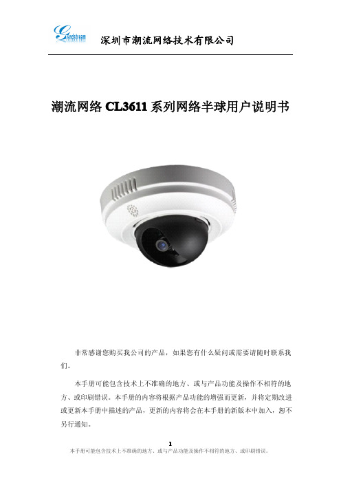
潮流网络CL3611系列网络半球用户说明书非常感谢您购买我公司的产品,如果您有什么疑问或需要请随时联系我们。
本手册可能包含技术上不准确的地方、或与产品功能及操作不相符的地方、或印刷错误。
本手册的内容将根据产品功能的增强而更新,并将定期改进或更新本手册中描述的产品,更新的内容将会在本手册的新版本中加入,恕不另行通知。
安全须知此内容的目的是确保用户正确使用本产品,以避免危险或财产损失。
在使用此产品之前,请认真阅读此说明手册并妥善保存以备日后参考。
如下所示,预防措施分为“警告”和“注意”两部分:警告:无视警告事项,可能会导致死亡或严重伤害。
注意:无视注意事项,可能会导致伤害或财产损失。
警告:1.请使用满足SELV(安全超低电压)要求的电源,并按照IEC60950-1符合Limited Power Source(有限电源)的额定电压为12V 直流电源供应。
2.如果设备工作不正常,请联系购买设备的商店或最近的服务中心,不要以任何方式拆卸或修改设备(未经许可的修改或维修所导致的问题,责任自负)。
3.为减少火灾或电击危险,请勿让本产品受到雨淋或受潮。
4.本安装应该由专业的服务人员进行,并符合当地法规规定。
5.应该在建筑物安装配线中组入易于使用的断电设备。
6.有关在天花板上安装设备的指示:安装后,请确保该连接至少可承受向下50牛顿(N)的拉力。
警告事项提醒用户防范潜在的死亡或严重伤害危险。
注意事项提醒用户防范潜在的伤害或财产损失危险。
注意:1.在让摄像机运行之前,请检查供电电源是否正确。
2.请勿将此产品摔落地下或受强烈敲击。
3.在对相机进行清洁时,请使用鼓风器除去镜头或滤光片上的尘埃;使用柔软、干燥的布清洁摄像机的外表面。
对于顽固的污迹,可使用蘸有少许清洁剂的软布将其拭去,然后将其擦干。
请勿使用挥发性溶剂,如酒精、苯、稀释剂等,以免损坏表面涂层。
4.避免对准强光(如灯光照明、太阳光等处)聚焦,否则容易引起过亮或拉光现象(这并非摄像机故障),也将影响CMOS寿命。
1SMA36AT3中文资料

120 = 10 µs 100 80 60 40 20 0 0.001 0.01 0.1 tP, PULSE WIDTH (ms) 1 10 TA = 25°C PW (ID) IS DEFINED AS THE POINT WHERE THE PEAK CURRENT PEAK VALUE DECAYS TO 50% OF Ipp. Ippm HALF VALUE – Ipp/2 10/1000 µs WAVEFORM AS DEFINED BY R.E.A. td 0 1 2 3 t, TIME (ms) 4 5
10,000 TJ = 25°C f = 1 MHz Vsig = 50 mVp–p
1,000
MEASURED AT ZERO BIAS
100
MEASURED AT STAND–OFF VOLTAGE, VWM
10 0 40 80 120 160 TA, AMBIENT TEMPERATURE (°C) 200 1 2 5 10 20 50 V(BR), BREAKDOWN VOLTAGE (VOLTS) 100 200
ELECTRICAL CHARACTERISTICS (VF = 3.5 Volts @ IF = 40 A for all types)
Reverse Stand–off Voltage VRWM (Volts) 5.0 6.0 6.5 7.0 7.5 8.0 8.5 9.0 Breakdown Voltage VBR Volts (Min) 6.4 6.67 7.22 7.78 8.33 8.89 9.44 10 IT mA 10 10 10 10 1 1 1 1 Maximum Reverse Voltage @ IRSM (Clamping Voltage) VRSM (Volts) 9.2 10.3 11.2 12.0 12.9 13.6 14.4 15.4 Maximum Reverse Surge Current IRSM (Amps) 43.5 38.8 35.7 33.3 31.0 29.4 27.8 26.0 Maximum Reverse Leakage @ VRWM IR (µA) 400 400 250 250 50 25 5.0 2.5 Devce D Marking
SN74ALS646A-1DWRG4,SN74ALS646ADWRG4,SN74ALS646A-1DW,SN74ALS646A-1DWE4, 规格书,Datasheet 资料

Addendum-Page 1PACKAGING INFORMATIONOrderable Device Status(1)Package Type PackageDrawingPins Package QtyEco Plan(2)Lead/Ball Finish MSL Peak Temp (3)Samples (Requires Login)5962-87595013A ACTIVE LCCC FK 281TBD Call TI Call TI 5962-8759501KA ACTIVE CFP W 241TBD Call TI Call TI 5962-8759501LA ACTIVE CDIP JT 241TBD Call TI Call TI 5962-89956013A ACTIVE LCCC FK 281TBD Call TI Call TI 5962-8995601LA ACTIVE CDIP JT 241TBD Call TI Call TI 5962-9052301LA ACTIVE CDIP JT 241TBD Call TI Call TISN54AS646JT ACTIVE CDIP JT 241TBDA42N / A for Pkg TypeSN74ALS646A-1DW ACTIVE SOIC DW 2425Green (RoHS & no Sb/Br)CU NIPDAU Level-1-260C-UNLIM SN74ALS646A-1DWE4ACTIVE SOIC DW 2425Green (RoHS & no Sb/Br)CU NIPDAU Level-1-260C-UNLIM SN74ALS646A-1DWG4ACTIVE SOIC DW 2425Green (RoHS & no Sb/Br)CU NIPDAU Level-1-260C-UNLIM SN74ALS646A-1DWR ACTIVE SOIC DW 24Green (RoHS & no Sb/Br)CU NIPDAU Level-1-260C-UNLIM SN74ALS646A-1DWRE4ACTIVE SOIC DW 24Green (RoHS & no Sb/Br)CU NIPDAU Level-1-260C-UNLIM SN74ALS646A-1DWRG4ACTIVE SOIC DW 24Green (RoHS & no Sb/Br)CU NIPDAU Level-1-260C-UNLIM SN74ALS646A-1NT ACTIVE PDIP NT 2415Pb-Free (RoHS)CU NIPDAU N / A for Pkg Type SN74ALS646A-1NTE4ACTIVE PDIP NT 2415Pb-Free (RoHS)CU NIPDAU N / A for Pkg Type SN74ALS646ADW ACTIVE SOIC DW 2425Green (RoHS & no Sb/Br)CU NIPDAU Level-1-260C-UNLIM SN74ALS646ADWE4ACTIVE SOIC DW 2425Green (RoHS & no Sb/Br)CU NIPDAU Level-1-260C-UNLIM SN74ALS646ADWG4ACTIVE SOIC DW 2425Green (RoHS & no Sb/Br)CU NIPDAU Level-1-260C-UNLIM SN74ALS646ADWR ACTIVE SOIC DW 242000Green (RoHS & no Sb/Br)CU NIPDAU Level-1-260C-UNLIM SN74ALS646ADWRE4ACTIVE SOIC DW 242000Green (RoHS & no Sb/Br)CU NIPDAU Level-1-260C-UNLIM SN74ALS646ADWRG4ACTIVESOICDW242000Green (RoHS & no Sb/Br)CU NIPDAU Level-1-260C-UNLIM芯天下--/Addendum-Page 2Orderable Device Status(1)Package Type PackageDrawingPins Package QtyEco Plan(2)Lead/Ball FinishMSL Peak Temp(3)Samples (Requires Login)SN74ALS646ANT ACTIVE PDIP NT 2415Pb-Free (RoHS)CU NIPDAU N / A for Pkg Type SN74ALS646ANTE4ACTIVE PDIP NT 2415Pb-Free (RoHS)CU NIPDAU N / A for Pkg Type SN74ALS648ADW ACTIVE SOIC DW 2425Green (RoHS & no Sb/Br)CU NIPDAU Level-1-260C-UNLIM SN74ALS648ADWE4ACTIVE SOIC DW 2425Green (RoHS & no Sb/Br)CU NIPDAU Level-1-260C-UNLIM SN74ALS648ADWG4ACTIVE SOIC DW 2425Green (RoHS & no Sb/Br)CU NIPDAU Level-1-260C-UNLIM SN74ALS648ANT ACTIVE PDIP NT 2415Pb-Free (RoHS)CU NIPDAU N / A for Pkg Type SN74ALS648ANTE4ACTIVE PDIP NT 2415Pb-Free (RoHS)CU NIPDAU N / A for Pkg Type SN74AS646DW ACTIVE SOIC DW 2425Green (RoHS & no Sb/Br)CU NIPDAU Level-1-260C-UNLIM SN74AS646DWE4ACTIVE SOIC DW 2425Green (RoHS & no Sb/Br)CU NIPDAU Level-1-260C-UNLIM SN74AS646DWG4ACTIVE SOIC DW 2425Green (RoHS & no Sb/Br)CU NIPDAU Level-1-260C-UNLIM SN74AS646NT ACTIVE PDIP NT 2415Pb-Free (RoHS)CU NIPDAU N / A for Pkg Type SN74AS646NTE4ACTIVE PDIP NT 2415Pb-Free (RoHS)CU NIPDAU N / A for Pkg Type SN74AS648DW ACTIVE SOIC DW 2425Green (RoHS & no Sb/Br)CU NIPDAU Level-1-260C-UNLIM SN74AS648DWE4ACTIVE SOIC DW 2425Green (RoHS & no Sb/Br)CU NIPDAU Level-1-260C-UNLIM SN74AS648DWG4ACTIVE SOIC DW 2425Green (RoHS & no Sb/Br)CU NIPDAU Level-1-260C-UNLIM SN74AS648NT ACTIVE PDIP NT 2415Pb-Free (RoHS)CU NIPDAU N / A for Pkg Type SN74AS648NT3OBSOLETE PDIP NT 24TBD Call TICall TISN74AS648NTE4ACTIVE PDIP NT 2415Pb-Free (RoHS)CU NIPDAU N / A for Pkg Type SNJ54ALS646FK ACTIVE LCCC FK 281TBD POST-PLATE N / A for Pkg TypeSNJ54ALS646JT ACTIVE CDIP JT 241TBD A42N / A for Pkg Type SNJ54ALS646W OBSOLETE CFP W 24TBD Call TI Call TI SNJ54ALS648FK OBSOLETE LCCC FK 24TBDCall TI Call TISNJ54ALS648JT ACTIVE CDIP JT 241TBD A42N / A for Pkg Type SNJ54ALS648WOBSOLETECFPW24TBDCall TICall TI芯天下--/Addendum-Page 3Orderable Device Status(1)Package Type PackageDrawingPins Package QtyEco Plan(2)Lead/Ball FinishMSL Peak Temp(3)Samples (Requires Login)SNJ54AS646FK ACTIVE LCCC FK 281TBD POST-PLATE N / A for Pkg TypeSNJ54AS646JT ACTIVE CDIP JT 241TBD A42N / A for Pkg Type SNJ54AS646WACTIVECFPW241TBDA42N / A for Pkg Type(1)The marketing status values are defined as follows:ACTIVE: Product device recommended for new designs.LIFEBUY: TI has announced that the device will be discontinued, and a lifetime-buy period is in effect.NRND: Not recommended for new designs. Device is in production to support existing customers, but TI does not recommend using this part in a new design.PREVIEW: Device has been announced but is not in production. Samples may or may not be available.OBSOLETE: TI has discontinued the production of the device.(2)Eco Plan - The planned eco-friendly classification: Pb-Free (RoHS), Pb-Free (RoHS Exempt), or Green (RoHS & no Sb/Br) - please check /productcontent for the latest availability information and additional product content details.TBD: The Pb-Free/Green conversion plan has not been defined.Pb-Free (RoHS): TI's terms "Lead-Free" or "Pb-Free" mean semiconductor products that are compatible with the current RoHS requirements for all 6 substances, including the requirement that lead not exceed 0.1% by weight in homogeneous materials. Where designed to be soldered at high temperatures, TI Pb-Free products are suitable for use in specified lead-free processes.Pb-Free (RoHS Exempt): This component has a RoHS exemption for either 1) lead-based flip-chip solder bumps used between the die and package, or 2) lead-based die adhesive used between the die and leadframe. The component is otherwise considered Pb-Free (RoHS compatible) as defined above.Green (RoHS & no Sb/Br): TI defines "Green" to mean Pb-Free (RoHS compatible), and free of Bromine (Br) and Antimony (Sb) based flame retardants (Br or Sb do not exceed 0.1% by weight in homogeneous material)(3)MSL, Peak Temp. -- The Moisture Sensitivity Level rating according to the JEDEC industry standard classifications, and peak solder temperature.Important Information and Disclaimer:The information provided on this page represents TI's knowledge and belief as of the date that it is provided. TI bases its knowledge and belief on information provided by third parties, and makes no representation or warranty as to the accuracy of such information. Efforts are underway to better integrate information from third parties. TI has taken and continues to take reasonable steps to provide representative and accurate information but may not have conducted destructive testing or chemical analysis on incoming materials and chemicals.TI and TI suppliers consider certain information to be proprietary, and thus CAS numbers and other limited information may not be available for release.In no event shall TI's liability arising out of such information exceed the total purchase price of the TI part(s) at issue in this document sold by TI to Customer on an annual basis.OTHER QUALIFIED VERSIONS OF SN54ALS646, SN54ALS648, SN54AS646, SN74AS646 :•Catalog: SN74ALS646, SN74ALS648, SN74AS646•Military: SN54AS646NOTE: Qualified Version Definitions:芯天下--/PACKAGE OPTION ADDENDUM16-Aug-2012Addendum-Page 4•Catalog - TI's standard catalog product•Military - QML certified for Military and Defense Applications芯天下--/TAPE AND REELINFORMATION*Alldimensions are nominalDevicePackage Type Package Drawing Pins SPQReel Diameter (mm)Reel Width W1(mm)A0(mm)B0(mm)K0(mm)P1(mm)W (mm)Pin1Quadrant SN74ALS646A-1DWR SOIC DW 240330.024.410.7515.7 2.712.024.0Q1SN74ALS646ADWRSOICDW242000330.024.410.7515.72.712.024.0Q116-Aug-2012*Alldimensions are nominalDevicePackage TypePackage DrawingPins SPQ Length (mm)Width (mm)Height (mm)SN74ALS646A-1DWR SOIC DW 240367.0367.045.0SN74ALS646ADWRSOICDW242000367.0367.045.016-Aug-2012IMPORTANT NOTICETexas Instruments Incorporated and its subsidiaries(TI)reserve the right to make corrections,enhancements,improvements and other changes to its semiconductor products and services per JESD46C and to discontinue any product or service per JESD48B.Buyers should obtain the latest relevant information before placing orders and should verify that such information is current and complete.All semiconductor products(also referred to herein as“components”)are sold subject to TI’s terms and conditions of sale supplied at the time of order acknowledgment.TI warrants performance of its components to the specifications applicable at the time of sale,in accordance with the warranty in TI’s terms and conditions of sale of semiconductor products.Testing and other quality control techniques are used to the extent TI deems necessary to support this warranty.Except where mandated by applicable law,testing of all parameters of each component is not necessarily performed.TI assumes no liability for applications assistance or the design of Buyers’products.Buyers are responsible for their products and applications using TI components.To minimize the risks associated with Buyers’products and applications,Buyers should provide adequate design and operating safeguards.TI does not warrant or represent that any license,either express or implied,is granted under any patent right,copyright,mask work right,or other intellectual property right relating to any combination,machine,or process in which TI components or services are rmation published by TI regarding third-party products or services does not constitute a license to use such products or services or a warranty or endorsement e of such information may require a license from a third party under the patents or other intellectual property of the third party,or a license from TI under the patents or other intellectual property of TI.Reproduction of significant portions of TI information in TI data books or data sheets is permissible only if reproduction is without alteration and is accompanied by all associated warranties,conditions,limitations,and notices.TI is not responsible or liable for such altered rmation of third parties may be subject to additional restrictions.Resale of TI components or services with statements different from or beyond the parameters stated by TI for that component or service voids all express and any implied warranties for the associated TI component or service and is an unfair and deceptive business practice. TI is not responsible or liable for any such statements.Buyer acknowledges and agrees that it is solely responsible for compliance with all legal,regulatory and safety-related requirements concerning its products,and any use of TI components in its applications,notwithstanding any applications-related information or support that may be provided by TI.Buyer represents and agrees that it has all the necessary expertise to create and implement safeguards which anticipate dangerous consequences of failures,monitor failures and their consequences,lessen the likelihood of failures that might cause harm and take appropriate remedial actions.Buyer will fully indemnify TI and its representatives against any damages arising out of the use of any TI components in safety-critical applications.In some cases,TI components may be promoted specifically to facilitate safety-related applications.With such components,TI’s goal is to help enable customers to design and create their own end-product solutions that meet applicable functional safety standards and requirements.Nonetheless,such components are subject to these terms.No TI components are authorized for use in FDA Class III(or similar life-critical medical equipment)unless authorized officers of the parties have executed a special agreement specifically governing such use.Only those TI components which TI has specifically designated as military grade or“enhanced plastic”are designed and intended for use in military/aerospace applications or environments.Buyer acknowledges and agrees that any military or aerospace use of TI components which have not been so designated is solely at the Buyer's risk,and that Buyer is solely responsible for compliance with all legal and regulatory requirements in connection with such use.TI has specifically designated certain components which meet ISO/TS16949requirements,mainly for automotive ponents which have not been so designated are neither designed nor intended for automotive use;and TI will not be responsible for any failure of such components to meet such requirements.Products ApplicationsAudio /audio Automotive and Transportation /automotiveAmplifiers Communications and Telecom /communicationsData Converters Computers and Peripherals /computersDLP®Products Consumer Electronics /consumer-appsDSP Energy and Lighting /energyClocks and Timers /clocks Industrial /industrialInterface Medical /medicalLogic Security /securityPower Mgmt Space,Avionics and Defense /space-avionics-defense Microcontrollers Video and Imaging /videoRFID OMAP Mobile Processors /omap TI E2E Community Wireless Connectivity /wirelessconnectivityMailing Address:Texas Instruments,Post Office Box655303,Dallas,Texas75265Copyright©2012,Texas Instruments Incorporated。
- 1、下载文档前请自行甄别文档内容的完整性,平台不提供额外的编辑、内容补充、找答案等附加服务。
- 2、"仅部分预览"的文档,不可在线预览部分如存在完整性等问题,可反馈申请退款(可完整预览的文档不适用该条件!)。
- 3、如文档侵犯您的权益,请联系客服反馈,我们会尽快为您处理(人工客服工作时间:9:00-18:30)。
SPEC NO: DSAD2247 APPROVED: WYNEC
REV NO: V.10 CHECKED: Joe Lee
DATE: MAR/29/2011 DRAWN: J.Yu
PAGE: 1 OF 6 ERP: 1301000352
芯天下--/
Selection Guide
Notes: 1.Wavelength: +/-1nm. 2. Forward Voltage: +/-0.1V.
Absolute Maximum Ratings at TA=25°C
Parameter Power dissipation DC Forward Current Peak Forward Current [1] Reverse Voltage Operating / Storage Temperature Lead Solder Temperature[2]
REV NO: V.10 CHECKED: Joe Lee
DATE: MAR/29/2011 DRAWN: J.Yu
ห้องสมุดไป่ตู้
PAGE: 3 OF 6 ERP: 1301000352
芯天下--/
PACKING & LABEL SPECIFICATIONS
SA36-11YWA
SPEC NO: DSAD2247 APPROVED: WYNEC
REV NO: V.10 CHECKED: Joe Lee
DATE: MAR/29/2011 DRAWN: J.Yu
PAGE: 2 OF 6 ERP: 1301000352
芯天下--/
Yellow
SA36-11YWA
SPEC NO: DSAD2247 APPROVED: WYNEC
Notes: 1. All dimensions are in millimeters (inches), Tolerance is ±0.25(0.01")unless otherwise noted. 2. The specifications, characteristics and technical data described in the datasheet are subject to change without prior notice.
9.14mm (0.36INCH) SINGLE DIGIT NUMERIC DISPLAY
Part Number: SA36-11YWA Yellow
Features
0.36 inch digit height. Low current operation. Excellent character appearance. Easy mounting on P.C. boards or sockets. Categorized for luminous intensity. Mechanically rugged. Standard : gray face, white segment. RoHS compliant.
Part No. Dice Lens Type Iv (ucd) [1] @ 10mA Min. SA36-11YWA Yellow (GaAsP/GaP) White Diffused 1400 Typ. 2600 Common Anode, Rt. Hand Decimal. Description
DATE: MAR/29/2011 DRAWN: J.Yu
PAGE: 5 OF 6 ERP: 1301000352
芯天下--/
SPEC NO: DSAD2247 APPROVED: WYNEC
REV NO: V.10 CHECKED: Joe Lee
DATE: MAR/29/2011 DRAWN: J.Yu
Description
The Yellow source color devices are made with Gallium Arsenide Phosphide on Gallium Phosphide Yellow Light Emitting Diode.
Package Dimensions& Internal Circuit Diagram
Notes: 1. 1/10 Duty Cycle, 0.1ms Pulse Width. 2. 2mm below package base.
Yellow 75 30 140 5 -40°C To +85°C 260°C For 3-5 Seconds
Units mW mA mA V
SPEC NO: DSAD2247 APPROVED: WYNEC
REV NO: V.10 CHECKED: Joe Lee
DATE: MAR/29/2011 DRAWN: J.Yu
PAGE: 4 OF 6 ERP: 1301000352
芯天下--/
SPEC NO: DSAD2247 APPROVED: WYNEC
REV NO: V.10 CHECKED: Joe Lee
Note: 1. Luminous intensity/ luminous Flux: +/-15%.
Electrical / Optical Characteristics at TA=25°C
Symbol λpeak λD [1] Δλ1/2 C VF [2] IR Parameter Peak Wavelength Dominant Wavelength Spectral Line Half-width Capacitance Forward Voltage Reverse Current Device Yellow Yellow Yellow Yellow Yellow Yellow Typ. 590 588 35 20 2.1 2.5 10 Max. Units nm nm nm pF V uA Test Conditions IF=20mA IF=20mA IF=20mA VF=0V;f=1MHz IF=20mA VR=5V
PAGE: 6 OF 6 ERP: 1301000352
芯天下--/