663856-000中文资料
MIL-S8TA 8-Port 10 100 1000 BASE-T 未管理开关用户指南(Rev.

MIL-S8TA8-Port 10/100/1000 BASE-T Unmanaged Switch User GuideRev. A22012-09-17Regulatory Approval- FCC Class A- UL 1950- CSA C22.2 No. 950- EN60950- CE- EN55022 Class A- EN55024Canadian EMI NoticeThis Class A digital apparatus meets all the requirements of the Canadian Interference-Causing Equipment Regulations.Cet appareil numerique de la classe A respecte toutes les exigences du Reglement sur le materiel brouilleur du Canada.European NoticeProducts with the CE Marking comply with both the EMC Directive (89/336/EEC) and the Low Voltage Directive (73/23/EEC) issued by the Commission of the European Community Compliance with these directives imply conformity to the following European Norms:EN55022 (CISPR 22) - Radio Frequency InterferenceEN61000-X - Electromagnetic ImmunityEN60950 (IEC950) - Product SafetyFive-Year Limited WarrantyTransition Networks warrants to the original consumer or purchaser that each of it's products,and all components thereof, will be free from defects in material and/or workmanship for aperiod of five years from the original factory shipment date. Any warranty hereunder isextended to the original consumer or purchaser and is not assignable.Transition Networks makes no express or implied warranties including, but not limited to, anyimplied warranty of merchantability or fitness for a particular purpose, except as expressly setforth in this warranty. In no event shall Transition Networks be liable for incidental orconsequential damages, costs, or expenses arising out of or in connection with theperformance of the product delivered hereunder. Transition Networks will in no case coverdamages arising out of the product being used in a negligent fashion or manner.TrademarksThe MiLAN logo and Transition Networks trademarks are registered trademarks of Transition Networks in the United States and/or other countries.To Contact Transition NetworksFor prompt response when calling for service information, have the following information ready:- Product serial number and revision- Date of purchase- Vendor or place of purchaseYou can reach Transition Networks technical support at:E-mail:**********************Telephone: +1.800.260.1312 x 200Fax: +1.952.941.2322Transition Networks6475 City West ParkwayEden Prairie, MN 55344United States of AmericaTelephone: +1.800.526.9267Fax: : +1.952.941.2322*******************© Copyright 2006 Transition NetworksThis equipment has been tested and found to comply with the limits for a class A device, pursuant to part 15 of the FCC rules. These limits are designed to provide reasonable protection against harmful interference in a commercial installation. This equipment generates uses and can radiate radio frequency energy and, if not installed and used in accordance with instructions, may cause harmful interference on radio communications. Operation of this equipment in a residential area is likely to cause harmful interference, in which case, the user will be requires to correct the interference at the user’s own expense.Content Introduction (1)Features (1)Package Contents (2)Hardware Description (3)Physical Dimensions (3)Front Panel (3)LEDs Indicators (3)Rear Panel (4)Installation (6)Attaching Rubber Feet (6)Mounting on the Wall (6)Power On (7)Technical Specification (8)IntroductionThe 8-port 10/100/1000BASE-T Switch with Auto MDI/MDIX is an unmanaged multi-port Switch that can be used to build high-performance switched networks. This switch is a store-and-forward device that offers low latency for high-speed networking. The Switch is designed for the core of the network backbone computing environment to solve traffic block problems at SME (small, medium enterprise) businesses.The 8-port 10/100/1000BASE-T Switch features a “store-and-forward”switching technology. This allows the switch to auto-learn and store source addresses in an 8K-entry MAC address table.Features⏹Conforms to IEEE 802.3, 802.3u, 802.3ab and 802.3x⏹8 Gigabit copper SOHO switch, compact size with universal internalpower⏹Auto-MDIX on all ports⏹16 Gbps back-plane⏹ N-Way Auto-Negotiation⏹8K MAC address table⏹Back pressure half duplex⏹Flow control full duplex⏹ Store-and-Forward switching architecture⏹ 144Kbytes memory buffer⏹True non-blocking switching⏹Support 8Kbytes Jumbo Frame1Package ContentsUnpack the contents of the switch and verify them against the checklist below.⏹ 8-port Switch⏹Power Cord.⏹User Guide.8-port Switch Power Cord User manualPackage ContentCompare the contents of your switch package with the standard checklist above. If any item is missing or damaged, please contact your local dealerfor service.23Hardware DescriptionPhysical DimensionsThe physical dimensions of the Switch is 165mm x 100mm x 32.5 mm (L x W x H)Front PanelThe front panel of the 8-Port Gigabit switch consists of LED-indicators (100/1000, Link/Activity, Full duplex/Collision) for each Gigabit port and power LED-indicator for unit.RJ-45 Ports (Auto MDI/MDIX): 8 10/100/1000 N-way auto-sensing for 10Base-T, 100Base-TX or 1000Base-T connections. (In general, MDI means connecting to another Hub or Switch while MDIX means connecting to a workstation or PC. Therefore, Auto MDI/MDIX allows you to connect to another Switch or workstation without changing to non-crossover or crossover cabling.)LEDs IndicatorsThe LED Indicators gives real-time information of systematic operation status. The following table provides descriptions of LED status and their meaning.Green PowerOnOff Power is not connectedGreen The port is operating at the speed of 1000Mbps.Orange The port is operating at the speed of 100Mbps.Off No device attached or in 10Mbps modeGreen The port is connecting with the device.Blinking The port is receiving or transmitting data.Off Nodeviceattached.Orange The port is operating in Full-duplex mode.Blinking Packet collision occurred on this port.Off No device attached or in half-duplex mode. Rear PanelThe rear panel of the 8-port Gigabit Switch consists of 8 auto-negotiation 10/100/1000Mbps Ethernet RJ-45 connectors (support Automatic4MDI/MDIX function).RJ-45 Ports (Auto MDI/MDIX): 8 port auto-negotiation 10/100/1000 Mbps Ethernet RJ-45 connectors[Auto MDI/MDIX means that you can connect to another Switch or workstation without changing non-crossover or crossover cabling.]5InstallationThis section shows the installation procedures of the switch.Set the Switch on a sufficiently large flat space with a power outlet nearby.The surface where you put your Switch should be clean, smooth, level, and sturdy. Make sure there is enough clearance around the Switch to allow attachment of cables, power cord and air circulation.Attaching Rubber FeetA. Make sure mounting surface on the bottom of the Switch is grease anddust free.B. Remove adhesive backing from your Rubber Feet.C. Apply the Rubber Feet to each corner on the bottom of the Switch.These footpads can prevent the Switch from shock/vibration. Mounting on the WallThe switch can be mounted on the wall. The switch has two wallmountbrackets included in the package.Power OnConnect the cord of power to the power socket on the rear panel of the Switch. The other side of power cord connects to the power outlet. Check the power indicator on the upper panel to see if power is properly supplied.7Technical SpecificationThe following table provides the technical specification of 8-ports Gigabit Switch.IEEE 802.3 10BASE-T EthernetIEEE 802.3u 100BASE-TX Fast EthernetIEEE 802.3ab Gigabit EthernetIEEE 802.3x Flow Control and Back-pressureCSMA/CDStore-and-Forward switching architecture14,880 pps for 10Mbps148,800 pps for 100Mbps1,488,000 pps for 1000MbpsRJ-45; Auto-MDIX on all ports8K Mac address table144Kbytes memory bufferSupports 8Kbytes jumbo packet size16Gbps810BASE-T: 2-pair UTP/STP Cat. 3, 4, 5 cable EIA/TIA-568 100-ohm (100m)100BASE-TX: 2-pair UTP/STP CAT. 5 cable EIA/TIA-568 100-ohm (100m)Gigabit Copper: 4 pair UTP/STP CAT. 5 cable EIA/TIA 568 100-ohm (100M)Per port: 100/1000, Link/Activity, Full duplex/ CollisionPer unit: PowerAC 110~240V, 50/60Hz7.6 Watt (maximum)0℃ to 45℃ (32℉ to 113℉)-40℃ to 70℃ (-40℉ to 158℉)10% to 90% (Non-condensing)0% to 95% (Non-condensing)165mm x 100mm x 32.5mm (L x W x H) Compliance with FCC Class A, CE Compliance UL, cUL,CE/EN609509。
美国AEMC公司高端和可移动数字弱电阻抗度计6550和6555产品说明书
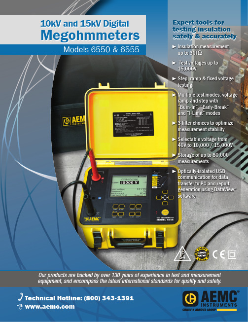
Technical Assistance (800) 343-1391 110kV and 15kV DigitalMegohmmetersModels 6550 & 6555► Insulation measurementup to 30T Ω► Test voltages up to 15,000V► Step, ramp & fixed voltagetesting► Multiple test modes: voltageramp and step with “Burn-In”, “Early-Break” and “I-Limit” modes► 3 filter choices to optimize measurement stability► Selectable voltage from40V to 10,000 / 15,000V ► Storage of up to 80,000 measurements► Optically-isolated USBcommunication for data transfer to PC and report generation using DataView ® softwareExpert tools for testing insulation safely & accuratelyIP 54Our products are backed by over 130 years of experience in test and measurement equipment, and encompass the latest international standards for quality and safety.Technical Hotline: (800) 343-13912 Technical Assistance (800) 343-1391Models 6550 & 6555HIGH-END & PORTABLEThe Megohmmeter Models 6550 and 6555 are high-end portable instruments intended for measuring a wide variety of electrical insulation resistance values oncables and devices operating at high voltage. They are packaged in a rugged case that is IP54 rated (cover closed). Test results and configuration information is provided on a graphical LCD screen, as well as exportable throughthe use of the DataView ® software provided. TheMegohmmeters can operate on battery or AC power while testing.These Megohmmeters contribute to the safety ofelectrical installations and equipment. Their operation is managed by microprocessors that acquire, process, display and store the measurements.The Model 6550 makes insulation measurements at voltages up to 10,000 V , the Model 6555 up to 15,000 V .Main Functions:• Detection and measurement of input voltage, frequency, and current prior to running a test.• Quantitative and qualitative insulation measurements.• Measurements at a fixed test voltage of 500, 1000, 2500, 5000, 10,000 or 15,000 V dc .• Measurements at an adjustable test voltagebetween 40 and 15,000 V dc preselected by the user prior to the test. Three preselected test voltages can be stored in the instrument and can be modified as needed prior to starting a test.IP 54• Ramp voltage measurements with a ramp from 40 to 10,000 V or 15,000 V , model dependent. Three ramp profiles can be stored in the instrument. Each ramp profile includes the starting and ending test voltage and the ramp time between the two.• Step voltage measurements with steps from 40 to 10,000 V or 15,000 V , model dependent.Three step voltage profiles can be stored in the instrument. Each contains up to 10 steps that include test voltage and duration.• Three test current choices: Burn-In, Early-Break and I-Limit provide qualitative analysis tools for detection breaks in insulation.• Quality ratio calculations for DAR, PI, and DD are calculated and displayed.• Temperature correction of the measured resistance to a reference temperature.• Capacitance measurement of the device tested.• Residual current measurement.Model 6555 checking insulation resistance on feed cables to a three-phase motor.Technical Assistance (800) 3►► SELECTABLE VOLTAGE FROM 40V TO 10kV / 15kV MODELSINSULATION TESTSTest VoltageAPPLICATIONS► Acceptance testing and preventive maintenance ► Test motors, cables, switchgears and wiring installations4 Technical Assistance (800) 343-1391CONTROL FEATURESFront Panel Features for Models 6550 & 6555Socket for connection to the ACpower and recharging of thebuilt-in batteriesmeasurementbuttonsUSB connector forcommunicationto a PC Seven position access to the fixed voltage, adjustable voltage,ramp and stepLarge, digital, backlit, Models 6550 and 6555 have the same front panel with differences in the display only .5Measurement Results Display AreaDisplay ofResultsTechnical Assistance (800) 5FUNCTIONSModels 6550 & 65556 Technical Assistance (800) 343-1391bargraphterminalsExample of display during measurement.resistanceresistance referred to the reference temperature.cursor Resistance versus time graph.This curve is useful primarily in the case of a measurement in V-RAMP mode.When Timed Run (test with programmed duration) or Timed Run + DD is selected, the duration of the measurement (m:s) can be set.The number of measurements that can be recorded depends on the number of samples stored for each measurement.quality ofof memory white).indicated.T est with programmed durationExample of display before measurement.FUNCTIONAL DISPLAYSSOFTWARE & ANALYSIS SCREENSEasy identification of all stored test results.Real-time display of measurement results.Step voltage set up screen.Technical Assistance (800) 7ORDERING INFORMATION M egohmmeter Model 6550 Ramp, StepV , Variable, Auto DAR/PI/DD, USB w/DataView Megohmmeter Model 6555 Ramp, StepV , Variable, Auto DAR/PI/DD, USB w/DataView AEMC ® Instruments • 15 Faraday Dr. • Dover, NH 03820 USA • (800) 343-1391•Fax(603)742-2346•E-mail:**************Export Department: +1 (603) 749-6434 x520 • Fax +1(603)742-2346•E-mail:***************© Chauvin Arnoux ®, Inc. d.b.a. AEMC ®Instruments Call the AEMC ® Instruments Technical Assistance Hotline for immediate consultation with an applications engineer: (800) 343-1391950.BR-6550-6555_0323 • Printed in the USA M u lt i-p u r p o s e C la m p -O n M e t e r s ca o tl in M E G O H MM E T E R SFo r a ll of y ou r I ns ul at io n Te st in g ne ed s...ch ni ca l H o tl in e: (800) 343-1391.a em c.co mP O W E R Q U A L I T Y Fo rA ll Y ou r Po w er Q ua li ty N ee ds ...Te 43-1391w w w ( Fo r a ll of yo ur G ro un d In te gr ity T es tin g ne ed s...G R O U N D R E S IS TA N C E T E S TE R S Te ch ni ca l H ot lin e: (800) 343-1391w w w .a em c.co mTEST & MEA SUREM ENT INSTR UMEN TSVOLUM E 23WWW.AEM TECHNICA L HOTLINE : (800) 343-1391Family of ProductsTo learn more, visit 。
GigaSPEED XL 3071E-B ETL Verified Category 6 U UTP
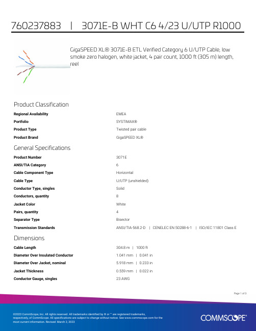
GigaSPEED XL® 3071E-B ETL Verified Category 6 U/UTP Cable, lowsmoke zero halogen, white jacket, 4 pair count, 1000 ft (305 m) length,reelProduct ClassificationRegional Availability EMEAPortfolio SYSTIMAX®Product Type Twisted pair cableProduct Brand GigaSPEED XL®General SpecificationsProduct Number3071EANSI/TIA Category6Cable Component Type HorizontalCable Type U/UTP (unshielded)Conductor Type, singles SolidConductors, quantity8Jacket Color WhitePairs, quantity4Separator Type BisectorTransmission Standards ANSI/TIA-568.2-D | CENELEC EN 50288-6-1 | ISO/IEC 11801 Class E DimensionsCable Length304.8 m | 1000 ftDiameter Over Insulated Conductor 1.041 mm | 0.041 inDiameter Over Jacket, nominal 5.918 mm | 0.233 inJacket Thickness0.559 mm | 0.022 inConductor Gauge, singles23 AWG13Page ofCross Section DrawingElectrical Specificationsdc Resistance Unbalance, maximum 5 %dc Resistance, maximum7.61 ohms/100 m | 2.32 ohms/100 ftDielectric Strength, minimum2500 VdcMutual Capacitance at Frequency 5.6 nF/100 m @ 1 kHzNominal Velocity of Propagation (NVP)70 %Operating Frequency, maximum300 MHzOperating Voltage, maximum80 VRemote Powering Fully complies with the recommendations set forth by IEEE 802.3bt (Type4) for the safe delivery of power over LAN cable when installed accordingto ISO/IEC 14763-2, CENELEC EN 50174-1, CENELEC EN 50174-2 or TIATSB-184-ASegregation Class cMaterial SpecificationsConductor Material Bare copperInsulation Material PolyolefinJacket Material Low Smoke Zero Halogen (LSZH)Separator Material PolyolefinPage of23Mechanical SpecificationsPulling Tension, maximum11.34 kg | 25 lbEnvironmental SpecificationsInstallation temperature0 °C to +60 °C (+32 °F to +140 °F)Operating Temperature-20 °C to +60 °C (-4 °F to +140 °F)Acid Gas Test Method EN 50267-2-3EN50575 CPR Cable EuroClass Fire Performance B2caEN50575 CPR Cable EuroClass Smoke Rating s1aEN50575 CPR Cable EuroClass Droplets Rating d0EN50575 CPR Cable EuroClass Acidity Rating a1Environmental Space Low Smoke Zero Halogen (LSZH)Smoke Test Method IEC 61034-2Packaging and WeightsCable weight38.097 kg/km | 25.6 lb/kftPackaging Type ReelRegulatory Compliance/CertificationsAgency ClassificationCENELEC EN 50575 compliant, Declaration of Performance (DoP) availableCHINA-ROHS Below maximum concentration valueISO 9001:2015Designed, manufactured and/or distributed under this quality management system REACH-SVHC Compliant as per SVHC revision on /ProductCompliance ROHSCompliantPage of33。
MSM6636中文资料

¡ SemiconductorMSM6636GENERAL DESCRIPTIONThe MSM6636 is a transmission controller for automotive LAN based on data communication protocol SAE-J1850. This LSI can realize a data bus topology bus LAN system with a PWM bit encoding method (41.6 K bps). In addition to a protocol control circuit, MSM6636 has an enclosed quartz oscillation circuit, host CPU interface (clock synchronous serial / UART), a transmit/receive buffer, and a bus receiver circuit that decreases the burden on the host CPU.FEATURES•Based on SAE-J1850 CLASS B DATA COMMUNICATION NETWORK INTERFACE (issued August 12, 1991)•CSMA/CD (Carrier-sense multiple access with collision detection)•Internal transmit buffer (1 frame) and receive buffer (2 frames)•Bit encoding: PWM (Pulse Width Modulation)•Transmission Speed: 41.6K bps•Multi-address setting with physical addressing: 1 type / functional addressing: 15 types •Address filter function by multi-addressing (broadcasting possible)•Automatic retransmission function by arbitration loss and non ACK •3 types of in-frame response support:q Single-byte response from a single recipientw Multi-byte response from a single recipient (with CRC code)e Single-byte response from multiple recipients (ID response as ACK)•Error detection by cyclic redundancy check (CRC)•Various communication error detections•Dual-wire bus abnormality detection by internal bus receiver and fault tolerance function •Host CPU interface is LSB first / serial, 4 modes supported q Clock synchronous serial (no parity)Normal mode:8-bit data MPC Mode:8-bit data + MPC bit (1: address / 0: data select bit)w UART (yes/no parity selectable)Normal mode: 1 start bit + 8-bit data + (parity) + 1 stop bit MPC mode: 1 start bit + 8-bit data + MPC bit + (parity) + 1 stop bit •Sleep FunctionLow current consumption mode by oscillation stop (IDS Max < 50µA)SLEEP / WAKE UP control from host CPU, WAKE UP via LAN bus •Available package 18pin DIP, 18 pin QFJ (PLCC) and 24pin SOP.¡ Semiconductor MSM6636SAE-J1850 Communication Protocol Conformity Transmission Controller for Automo-tive LANMSM6636¡ Semiconductor BLOCK DIAGRAM¡ Semiconductor MSM6636PIN CONFIGURATION (TOP VIEW)PIN DESCRIPTIONPin Name I/O FunctionAVDD 1—Analog power supply pin BO –2O LAN - BUS output –BI –3I BI +4I BO +5O AGND 9—Analog ground pin U - C 10I 0: UART1: clock synchronous serial select pinM - N 11I 0: MPC mode 1:normal mode select pinDGND 12—Digital ground pin OSC 113O Crystal oscillation output OSC 014I Crystal oscillation input A - D 15I 0: data communication 1: address communication SCLK / PAE 16I Serial clock input/Parity select pin RXD 20I Serial data input pin TXD 21O Serial data output pin INT 22O Interrupt output pin RES 23I Reset input pin DVDD24—Digital power supply pinPin #123456789101112131415161718DIP/QFJ SOP LAN - BUS input –LAN - BUS input +LAN - BUS output +18pin Plastic DIP AVDD DVDD BO–RES BI–INT BI+TXD BO+RXD AGND SCLK /PAE U-C A-D M-NOSC0DGND OSC1BI– INT BI+TXD BO+RXD AGND SCLK /PAE U-CA-DB O –M -N A V D D D G N D D V D D O SC 1R E SO S C 018pin Plastic QFJ AVDD DVDD BO–RES BI–INT BI+TXD BO+RXD NC NC NC NC NC NCAGND SCLK/PAE U-C A-D M-N OSC0DGNDOSC124pin Plastic SOPNC: No Connection123456789876543210111111*********891011345671615141312123456789101112242322212019181716151413MSM6636¡ SemiconductorABSOLUTE MAXIMUM RATINGSParameter Symbol ConditionRated Value Unit Power Supply VoltageDVDD, AVDD-0.3~7.0V Input Voltage V I -0.3~DVDD+0.3V Output Voltage V O -0.3~DVDD+0.3V P D(DIP)*1Ta = 25°C 860mW Storage TemperatureT STG-55~150°CDGND = AGND = 0VAVDD = DVDD AVDD = DVDD Power Dissipation P D(QFJ)*2Ta = 25°C 960mW P D(SOP)*3Ta = 25°C 830mW P D(DIP)*1:18PIN DIP package power dissipation P D(QFJ)*2:18PIN QFJ package power dissipation PD(SOP)*3:24PIN SOP package power dissipation Power Dissipation Curve1000860500-4025125150Ambient temperature Ta (°C)P o w e r d i s s i p a t i o n P D (D I P) [m W ]1000960500-4025125150Ambient temperature Ta (°C)P o w e r d i s s i p a t i o n P D (Q F J ) [m W ]1000830500-4025125150Ambient temperature Ta (°C)P o w e r d i s s i p a t i o n P D (S O P ) [m W ]< 24PIN SOP package >< 18PIN DIP package >< 18PIN QFJ package >¡ Semiconductor MSM6636 OPERATION RANGEParameter Symbol Condition Rated Value Unit Power Supply Voltage DVDD, AVDD AVDD = DVDD 4.5~5.5VOperating Frequency f OSC DVDD = AVDD = 5V±10%2~16MHzOperating Temperature Ta-40~+125°CDGND = AGND = 0VELECTRICAL CHARACTERISTICSDC CharacteristicsH Level Input Voltage V IH1—A DVDD ¥ 0.8—DVDD + 0.3VParameter Symbol Condition Application MIN TYP MAX Unit L Level Input Voltage V IL1—A DGND - 0.3—DVDD ¥ 0.2VH Level Input Current I IH1V I = V DD B——+1µAL Level Input Current I IL1V I = 0V B——- 1µAH Level Input Current I IH2V I = V DD C——+1µAL Level Input Current I IL2V I = 0V C——- 100µAH Level Input Current I IH3V I = V DD BI (+)——+ 100µAL Level Input Current I IL3V I = 0V BI (-)——- 100µAH Level Output Voltage V OH1I O = -400µA D DVDD - 0.4——VL Level Output Voltage V OL1I O = +3.2mA D——DGND + 0.4VH Level Output Voltage V OH2I O = -4.0mA E DVDD - 0.4——VL Level Output Voltage V OL2I O = +4.0mA E——DGND + 0.4VCurrent Consumption 1I DS During sleep——50µACurrent Consumption 2I DD f = 16MHz,no load——10mA DVDD = AVDD = 5V±10%, DGND = AGND = 0V, Ta = -40 ~ +125°CH Level Input Voltage V IH2—F DVDD - 2.0—DVDD + 1.0VL Level Input Voltage V IL2—F DGND - 1.0—DGND + 2.0V Receiver Hysteresis Width V H—F100—400mVGND Offset Voltage V OFF——±1V————A: RES, SCLK/PAE, RXD, U-C, M-N, A-D, OSC0B: SCLK/PAE, RXD, U-C, M-N, A-DC: RESD: TXD, INTE: BO-, BO+F: BI-, BI+MSM6636¡ SemiconductorAC Chacteristics PWM Bit Timingmin typ max min max Bit Length TP123.6424.0024.3621.0028.00µs Parameter Symbol TransmitReceive Unit "1" Dominant Width TP2 6.907.007.11 5.0012.00µs "0" Dominant Width TP314.8715.0015.2313.0020.00µs "SOF" Dominant Width TP430.5431.0031.4729.0036.00µs "SOF,BRK" Length TP547.2848.0048.7245.0052.00µs "BRK" Dominant Width TP638.4239.0039.5937.0044.00µs "EOD" + Bit Length TP747.2848.0048.7243.0051.00µs "EOF" + Bit Length TP870.9272.00—69.0076.00µs "0" Passive WidthTP108.869.009.144.0015.00µs"EOF + IFS" + Bit Length TP994.5696.00—86.00—µs Note:DVDD = AVDD = 5 V ± 10%, Ta = -40 ~ +125˚C, In setting 41.6 K bpsDominantPassive " 1 "DominantPassive" 0 "DominantPassive" SOF "" EOD "DominantPassiveDominantPassive" BRK "" EOF "" IFS "Dominant Passive¡ Semiconductor MSM6636CPU Serial Interface Timing m Clock synchronous SerialOSCO (source oscillation) Pulse Cycle tø62500ns ParameterSymbol Min Typ Max Unit SCLK-L Interval Width t CKLW 8tø—ns SCLK-H Interval Width t CKHW 8tø—ns SCLK ≠ - RXD Setup Time t SRS 4tø—ns SCLK ≠ - RXD Hold Time t SRH 4tø—ns SCLK ≠ - TXD Output Delay Time t STD 4tø6tø + 100ns A-D - SCLK ≠ Setup Time t AS 0—ns SCLK ≠ - A-D Hold Time t AH 8tø—ns SCLK Frame Interval Time *1t INT18tø—ns SCLK Frame Interval Time *2t INT216tø—nsDVDD=AVDD=5V±10%, Ta =-40~+125°C——————————SCLK Frame Interval Time *1Between “Communication type (WR) and address setting” frame and “WR data” frame.Between “WR data” frame and “WR data” frame during continuous WR.SCLK Frame Interval Time *2Between “Communication type (RD) and address setting” frame and “RD data” frame.Between “RD data” frame and “RD data” frame during continuous RD.MSM6636¡ Semiconductorm UARTA-D - STOP bit ≠ Setup Time t UAS 0—ns ParameterSymbol Min Typ Max Unit STOP bit Ø – A-D Hold Time t UAH 0—ns START bit Ø – TXD Output Delay Time t UTD 48tø50tø + 100ns Write Frame Interval Time *3t INT30—ns Read Frame Interval Time *4t INT410tø—nsDVDD=AVDD=5V±10%, Ta =-40~+125°C—————Write Frame Interval Time *3Between “Communication type (WR) and address setting” frame and “WR data” frame.Between “WR data” frame and “WR data” frame during continuous WR.Read Frame Interval Time *4Between “Communication type (RD) and address setting” frame and “RD data” frame.¡ Semiconductor MSM6636Wakeup Input SignalLAN bus Passive Æ Dominant Change Pulse Width t WD 7—µs ParameterSymbol Min Typ Max Unit RXD Terminal Input Pulse Width t WR 300—ns Bus Receiver Stable Time *5t RS1—µsDVDD=AVDD=5V±10%, Ta =-40~+125°C———OSC0A-D RXDTXDNote: The time chart shows the wakeup input signals from each sleep status Bus Receiver Stable Time *5The stable time of the bus receiver is from just after wakeup to the restart of message trans-mission and reception. However, the clock oscillation source should use an external clock.(A clock is input even in the sleep status.)MSM6636¡ SemiconductorFault Tolerant Function Operation ConditionsLAN bus (+) GND Short Circuit Detection Pulse Width t PG5—µs ParameterSymbol Min Typ Max Unit LAN bus (+) VDD Short Circuit Detection Pulse Width t PV 48—µs LAN bus (-) VDD Short Circuit Detection Pulse Widtht NV5—µsDVDD=AVDD=5V±10%, Ta =-40~+125°C, In setting 41.6Kbps———LAN bus (-) GND Short Circuit Detection Pulse Width t NG 48—µs —BUS(+)BUS(-)BUS(+)BUS(-)Reset Input Pulse WidthReset Input Pulse Widtht RES0.1—µsParameterSymbol Min Typ Max Unit DVDD=AVDD=5V±10%, Ta=–40~+125°C—RES¡ Semiconductor MSM6636 APPLICATION EXAMPLEHost CPU and LAN bus Connection ExampleHost CPU and LAN bus connection example of MSM6636 is shown below.The above connection example is when "UART, MPC and parity no mode" was used as the "host CPU interface, and when CLKOUT output of the host CPU" was used as the clock for MSM6636.Depending on the control target, an optimum host CPU (number of ports, A/D converter yes / no) can be selected, and an optimum system can be constructed.11。
Mare Nostrum SP液体说明书

Mare Nostrum SP液体。
产品名称产品类型应急咨询电话(带值班时间):::企业标识:化学品的推荐用途和限制用途产品代码:8080游艇全效自抛光防污漆产品描述:油漆。
用于涂料 - Consumer use: 本产品的使用必须符合标签说明。
用于涂料 - 用于专业领域佐敦涂料(张家港)有限公司中国江苏扬子江国际化学工业园南海路39号 215634电话: +86 512 58937988传真: +86 512 58937986Jotun Coatings (Zhangjiagang) Co. LtdNO.39 Nanhai Road Jiangsu Yangtze River International Chemical Industry Park,Jiangsu Province 215634 China Tel: +86 512 58937988Fax: +86 512 58937986中远佐敦船舶涂料(青岛)有限公司中国山东省青岛市高新区春阳路800号总机电话: +86-532-68689888总机传真: +86-532-66726750Jotun COSCO Marine Coatings (Qingdao) Co. Ltd.No. 800, Chunyang Road, High-tech Zone, Qingdao, P. R. China Tel: +86-532-68689888Fax: +86-532-66726750******************中国化学事故应急服务 Tel: +86 532 83889090易燃液体 - 类别 3急性毒性 (口服) - 类别 5皮肤腐蚀/刺激 - 类别 3严重眼损伤/眼刺激 - 类别 1皮肤致敏物 - 类别 1致癌性 - 类别 2特异性靶器官毒性 一次接触 (呼吸道刺激) - 类别 3特异性靶器官毒性 一次接触 (麻醉效应) - 类别 3危害水生环境一急性危险 - 类别 1危害水生环境一长期危险 - 类别 1GHS危险性类别:物质或混合物的分类根据 GB13690-2009 和 GB30000-2013警示词:危险.危险性说明:H226 - 易燃液体和蒸气。
扬子石化—巴斯夫有限责任公司 Diethylenetriamine 说明书
安全技术说明书页: 1/11 扬子石化—巴斯夫有限责任公司安全技术说明书日期 / 修订: 09.09.2010版本: 7.1产品: Diethylenetriamine(30036876/SDS_GEN_CN/ZH)印刷日期 02.06.20111. 物质/制剂及公司信息Diethylenetriamine推荐用途和限制用途: 工业化学品公司:扬子石化—巴斯夫有限责任公司江苏省南京市六合区新华东路8号邮政编码 210048电话: +86 25 5773-6769传真号: +86 25 5856-9278E-mail地址: ******************.cn紧急联络信息:扬子石化—巴斯夫有限责任公司紧急响应中心(中国, 南京)电话: +86 25 5856-2402传真号: +86 25 5856-9077Company:BASF-YPC Company LimitedLuhe District,Nanjing,JiangsuPostal Code:210048, CHINA Telephone: +86 25 5773-6769 Telefax number: +86 25 5856-9278E-mail address: ******************.cnEmergency information:BYC ERC(China,Nanjing) Telephone: +86 25 5856-2402 Telefax number: +86 25 5856-90772. 危险性识别纯物质和混合物的分类:急性毒性: 分类4 (口服)急性毒性: 分类3 (皮肤接触)皮肤腐蚀/刺激: 分类1B皮肤致敏物: 分类1对水环境的急性危害: 分类3扬子石化—巴斯夫有限责任公司安全技术说明书日期 / 修订: 09.09.2010版本: 7.1产品: Diethylenetriamine(30036876/SDS_GEN_CN/ZH)印刷日期 02.06.2011标签要素和警示性说明:警示词:危险危险性说明:可导致严重的皮肤灼伤及眼睛损伤。
UL2556中文翻译

UL2556 2011译版通过UL UL安全标准的保护。
既不是一个标准的打印副本,也分布一个标准的软盘和分布软盘上的标准文件的软盘应以任何方式改变。
所有UL的标准和所有,所有权,和权利有关这些标准应保持了UL的唯一和排他性的财产。
保留所有权利。
本出版物的任何部分进行复制,存储在检索系统中,或任何形式的任何手段,电子,机械复印,录音,或以其他方式传播未经事先批准的UL。
UL安全标准的修订,不时发出。
一个是最新的UL安全标准只有当它采用了最近通过的修订。
UL提供本标准平方米²,没有任何形式的的担保,明示或暗示,包括但不限于对适销性或为任何目的的隐含担保。
在任何情况下,UL认证的任何特殊,偶然,必然,间接或类似的损害承担责任,包括利润损失,储蓄损失,数据丢失,或任何因使用或其他损害无法使用这个标准,即使UL或授权的UL代表的建议这种损害的可能性。
在任何情况下,UL的任何损害赔偿责任,不断超过支付的价格这个标准,无论索赔的形式。
UL将尝试回答有关其标准的电子版本的支持请求。
然而,这支持服务是提供一个合理的努力的基础上,和UL未必能解决所有支持请求。
只有他们正在使用的UL认证支持其标准的电子版本条件和操作系统,它的目的是。
UL的扶持政策可能会改变时间到时,恕不另行通知。
UL保留权利更改的格式,简报,文件类型和格式,交货方式和格式,和它的印刷版和电子标准,恕不另行通知。
UL安全标准的电子版本,买方同意维护,保障,并举行UL认证无害和反对任何损失,费用,责任,损失,索赔,或判决(包括合理的律师费)引入任何错误或偏差造成的,而买方存储购买者的计算机系统上的电子标准。
如果购买一个单用户版电子标准,本标准的一个副本可以存储在一台个人计算机的硬盘,或在一个单一的局域网的文件服务器或永久存储在这种方式的多用户电脑设备,这一标准只能由一个用户访问的时间和为没有多个并发访问的可能性。
如果多用户版电子标准购买,可以存储在一个标准的副本一个单一的局域网文件服务器,或在多用户计算机的永久性存储设备,或Intranet 服务器。
5082-3353-CC000中文资料

Features• Low Power Consumption • Industry Standard Size• Industry Standard Pinout • Choice of Character Size7.6 mm (0.30 in), 10 mm (0.40 in), 10.9 mm (0.43 in), 14.2 mm (0.56 in), 20 mm (0.80 in)• Choice of ColorsAlGaAs Red, High Efficiency Red (HER), Yellow, Green• Excellent Appearance Evenly Lighted Segments±50° Viewing Angle• Design FlexibilityCommon Anode or Common CathodeSingle and Dual DigitLeft and Right Hand Decimal Points±1. Overflow Character• Categorized for Luminous IntensityYellow and Green Categorized for ColorUse of Like Categories Yields a Uniform Display• Excellent for Long Digit String Multiplexing DescriptionThese low current seven segment displays are designed for applica-tions requiring low power consumption. They are tested and selected for their excellent low current characteristics to ensure that the segments are matched at low currents. Drive currents as low as 1 mA per segment are available.Pin for pin equivalent displays are also available in a standard current or high light ambient design. The standard current displays are available in all colors and are ideal for most applica-tions. The high light ambient displays are ideal for sunlight ambients or long string lengths. For additional information see the 7.6 mm Micro Bright Seven Segment Displays, 10 mm Seven Segment Displays, 7.6 mm/10.9 mm Seven Segment Displays, 14.2 mm Seven Segment Displays, 20 mm Seven Segment Displays, or High Light Ambient Seven Segment Displays data sheets.Low Current Seven SegmentDisplays Technical Data HDSP-335x SeriesHDSP-555x SeriesHDSP-751x SeriesHDSP-A10x Series HDSP-A80x Series HDSP-A90x Series HDSP-E10x Series HDSP-F10x Series HDSP-G10x Series HDSP-H10x Series HDSP-K12x, K70x Series HDSP-N10x SeriesHDSP-N40x SeriesDevicesAlGaAs HER Yellow Green Package HDSP-HDSP-HDSP-HDSP-Description Drawing A1017511A801A9017.6 mm Common Anode Right Hand Decimal A A1037513A803A9037.6 mm Common Cathode Right Hand Decimal B A1077517A807A9077.6 mm Common Anode ±1. Overflow C A1087518A808A9087.6 mm Common Cathode ±1. Overflow D F10110 mm Common Anode Right Hand Decimal E F10310 mm Common Cathode Right Hand Decimal F F10710 mm Common Anode ±1. Overflow G F10810 mm Common Cathode ±1. Overflow H G10110 mm Two Digit Common Anode Right Hand Decimal X G10310 mm Two Digit Common Cathode Right Hand Decimal Y E100335010.9 mm Common Anode Left Hand Decimal I E101335110.9 mm Common Anode Right Hand Decimal J E103335310.9 mm Common Cathode Right Hand Decimal K E106335610.9 mm Universal ±1. Overflow[1]L H101555114.2 mm Common Anode Right Hand Decimal M H103555314.2 mm Common Cathode Right Hand Decimal N H107555714.2 mm Common Anode ±1. Overflow O H108555814.2 mm Common Cathode ±1. Overflow P K121K70114.2 mm Two Digit Common Anode Right Hand Decimal R K123K70314.2 mm Two Digit Common Cathode Right Hand Decimal S N10020 mm Common Anode Left Hand Decimal Q N101N40120 mm Common Anode Right Hand Decimal T N103N40320 mm Common Cathode Right Hand Decimal U N10520 mm Common Cathode Left Hand Decimal V N106N40620 mm Universal ±1. Overflow[1]W Note:1. Universal pinout brings the anode and cathode of each segment’s LED out to separate pins. See internal diagrams L or W.Part Numbering System5082-x xx x-x x x xxHDSP-x xx x-x x x xxMechanical Options[1]00: No mechanical optionColor Bin Options[1,2]0: No color bin limitationMaximum Intensity Bin[1,2]0: No maximum intensity bin limitationMinimum Intensity Bin[1,2]0: No minimum intensity bin limitationDevice Configuration/Color[1]G: GreenDevice Specific Configuration[1]Refer to respective datasheetPackage[1]Refer to Respective datasheetNotes:1. For codes not listed in the figure above, please refer to the respective datasheet or contact your nearest Agilent representative fordetails.2. Bin options refer to shippable bins for a part-number. Color and Intensity Bins are typically restricted to 1 bin per tube (excep-tions may apply). Please refer to respective datasheet for specific bin limit information.Package DimensionsPackage Dimensions (cont.)Package Dimensions (cont.)*The Side View of package indicates Country of Origin.Package Dimensions (cont.)Package Dimensions (cont.)Package Dimensions (cont.)Internal Circuit DiagramInternal Circuit Diagram (cont.)Absolute Maximum RatingsAlGaAs Red - HDSP-HERA10X/E10X/H10X HDSP-751X/Yellow GreenK12X/N10X/N40X335X/555X/HDSP-A80X HDSP-A90X Description F10X, G10X Series K70X Series Series Series Units Average Power per Segment or DP375264mW Peak Forward Current per 45mA Segment or DPDC Forward Current per15[1]15[2]mA Segment or DPOperating Temperature Range-20 to +100-40 to +100°C Storage Temperature Range -55 to +100°C Reverse Voltage per Segment 3.0V or DPWave Soldering Temperature for 3Seconds (1.60 mm [0.063 in.] below 250°C seating body)Notes:1. Derate above 91°C at 0.53 mA/°C.2. Derate HER/Yellow above 80°C at 0.38 mA/°C and Green above 71°C at 0.31 mA/°C.Electrical/Optical Characteristics at T A = 25°CAlGaAs RedDeviceSeriesHDSP-Parameter Symbol Min.Typ.Max.Units Test Conditions315600I F = 1 mA A10x3600I F = 5 mA330650I F = 1 mAF10x, G10x3900I F = 5 mA390650I F = 1 mA E10x Luminous Intensity/Segment[1,2]I Vµcd(Digit Average)3900I F = 5 mA400700I F = 1 mAH10x, K12x4200I F = 5 mA270590I F = 1 mAN10x, N40x3500I F = 5 mA1.6I F = 1 mAForward Voltage/Segment or DP V F 1.7V I F = 5 mA1.82.2I F = 20 mA PkAll Devices Peak WavelengthλPEAK645nmDominant Wavelength[3]λd637nmReverse Voltage/Segment or DP[4]V R 3.015V I R = 100 µATemperature Coefficient of∆V F/°C-2 mV mV/°CV F/Segment or DPA10x255F10x, G10x320E10x340Thermal Resistance LED RθJ-PIN°C/W/SegH10x, K12x Junction-to-Pin400N10x, N40x430High Efficiency RedDeviceSeriesHDSP-Parameter Symbol Min.Typ.Max.Units Test Conditions160270I F = 2 mA 751x1050I F = 5 mA200300I F = 2 mA Luminous Intensity/Segment[1,2]I V mcd(Digit Average)1200I F = 5 mA335x, 555x,K70x270370I F = 2 mA1480I F = 5 mA1.6I F = 2 mAForward Voltage/Segment or DP V F 1.7V I F = 5 mA2.1 2.5I F = 20 mA Pk All Devices Peak WavelengthλPEAK635nmDominant Wavelength[3]λd626nmReverse Voltage/Segment or DP[4]V R 3.030V I R = 100 µATemperature Coefficient of∆V F/°C-2mV/°CV F/Segment or DP751x200335x Thermal Resistance LED RθJ-PIN280°C/WJunction-to-Pin555x, K70x345YellowDeviceSeriesHDSP-Parameter Symbol Min.Typ.Max.Units Test Conditions Luminous Intensity/Segment[1,2]250420I F = 4 mA(Digit Average)I V mcd1300I F = 10 mA1.7I F = 4 mAForward Voltage/Segment or DP V F 1.8V I F = 5 mA A80x2.1 2.5I F = 20 mA PkPeak WavelengthλPEAK583nmDominant Wavelength[3,5]λd581.5585592.5nmReverse Voltage/Segment or DP[4]V R 3.030V I R = 100 µATemperature Coefficient of∆V F/°C-2mV/°CV F/Segment or DPThermal Resistance LED RθJ-PIN200°C/WJunction-to-PinGreenDeviceSeriesHDSP-Parameter Symbol Min.Typ.Max.Units Test Conditions Luminous Intensity/Segment[1,2]250475I F = 4 mA(Digit Average)I V mcd1500I F = 10 mA1.9I F = 4 mAForward Voltage/Segment or DP V F 2.0V I F = 10 mA A90x2.1 2.5I F = 20 mA PkPeak WavelengthλPEAK566nmDominant Wavelength[3,5]λd571577nmReverse Voltage/Segment or DP[4]V R 3.030V I R = 100 µATemperature Coefficient of∆V F/°C-2mV/°CV F/Segment or DPThermal Resistance LED RθJ-PIN200°C/WJunction-to-PinNotes:1. Device case temperature is 25°C prior to the intensity measurement.2. The digits are categorized for luminous intensity. The intensity category is designated by a letter on the side of the package.3. The dominant wavelength, λd, is derived from the CIE chromaticity diagram and is the single wavelength which defines the color of thedevice.4. Typical specification for reference only. Do not exceed absolute maximum ratings.5. The yellow (HDSP-A800) and Green (HDSP-A900) displays are categorized for dominant wavelength. The category is designated by anumber adjacent to the luminous intensity category letter.AlGaAs RedIntensity Bin Limits (mcd)AlGaAs RedHDSP-A10xIV Bin Category Min.Max.E0.3150.520F0.4280.759G0.621 1.16H0.945 1.71I 1.40 2.56J 2.10 3.84K 3.14 5.75L 4.708.55HDSP-E10x/F10x/G10xIV Bin Category Min.Max.D0.3910.650E0.5320.923F0.755 1.39G 1.13 2.08H 1.70 3.14HDSP-H10x/K12xIV Bin Category Min.Max.C0.4150.690D0.5650.990E0.810 1.50F 1.20 2.20G 1.80 3.30H 2.73 5.00I 4.097.50HDSP-N10xIV Bin Category Min.Max.A0.2700.400B0.3250.500C0.4150.690D0.5650.990E0.810 1.50F 1.20 2.20G 1.80 3.30H 2.73 5.00I 4.097.50Intensity Bin Limits (mcd), continued HERHDSP-751xIV Bin Category Min.Max.B0.1600.240C0.2000.300D0.2500.385E0.3150.520F0.4280.759G0.621 1.16HDSP-751xIV Bin Category Min.Max.B0.2400.366C0.3000.477D0.3910.650E0.5320.923F0.755 1.39G 1.13 2.08H 1.70 3.14HDSP-555x/K70xIV Bin Category Min.Max.A0.2700.400B0.3250.500C0.4150.690D0.5650.990E0.810 1.50F 1.20 2.20G 1.80 3.30H 2.73 5.00I 4.097.50Intensity Bin Limits (mcd), continued YellowHDSP-A80xIV Bin Category Min.Max.D0.2500.385E0.3150.520F0.4250.760G0.625 1.14H0.940 1.70I 1.40 2.56J 2.10 3.84K 3.14 5.76L 4.718.64M7.0713.00N10.6019.40O15.9029.20P23.9043.80Q35.8065.60GreenHDSP-A90xIV Bin Category Min.Max.E0.3150.520F0.4250.760G0.625 1.14H0.940 1.70I 1.40 2.56J 2.10 3.84K 3.14 5.76L 4.718.64M7.0713.00N10.6019.40O15.9029.20P23.9043.80Q35.8065.60Electrical/OpticalFor more information on electrical/optical characteristics, please see Application Note 1005.Contrast Enhancement For information on contrast enhancement, please see Application Note 1015.Soldering/Cleaning Cleaning agents from the ketone family (acetone, methyl ethyl ketone, etc.) and from the chorinated hydrocarbon family (methylene chloride, trichloro-ethylene, carbon tetrachloride, etc.) are not recommended for cleaning LED parts. All of these various solvents attack or dissolve the encapsulating epoxies used to form the package of plastic LED parts.For information on soldering LEDs, please refer to Application Note 1027.Note:All categories are established for classification of products. Productsmay not be available in all categories. Please contact your localAgilent representatives for further clarification/information.Color Categories/semiconductorsFor product information and a complete list ofdistributors, please go to our web site.For technical assistance call:Americas/Canada: +1 (800) 235-0312 or(916) 788 6763Europe: +49 (0) 6441 92460China: 10800 650 0017Hong Kong: (+65) 6271 2451India, Australia, New Zealand: (+65) 6271 2394Japan: (+81 3) 3335-8152(Domestic/International), or0120-61-1280(Domestic Only)Korea: (+65) 6271 2194Malaysia, Singapore: (+65) 6271 2054Taiwan: (+65) 6271 2654Data subject to change.Copyright © 2005 Agilent Technologies, Inc.Obsoletes 5988-8412ENJanuary 19, 20055989-0080EN。