08_High-Aspect-Ratio Copper-Via-Filling for Three-Dimensional Chip Stacking_ECS2005
Plated and filled Via-in-Pad

A p p l i c a t i o n N o t eP l a t e d a n d F i l l e d V i a-I n-P a d,a n d o t h e rV i a C a p p i n g M e t h o d sIncreases in printed circuit board density and the need for higher electrical performance have resulted in several design challenges. Some of these challenges are related to the proximity of the vias to the surface mount (SMT) and ball grid array (BGA) lands. To reduce inductance, increase density or employ finer pitch array packages, via pads are being placed close to the SMT/BGA lands. Increases in board thickness, due to higher I/O array packages complicate these issues as larger holes and pads may be required to maintain through-hole reliability. Other design factors such as placing passive devices directly under packages have led for the need for improved Via-in-Pad technology. Many designers are searching for solutions to these complex issues.This application note will cover new approaches such as plated and filled Via-in-Pad along with the more common methods used to reduce the SMT/BGA land to via pad distance while reducing the risk of solder loss down the via during printed circuit assembly. These methods are also used on some designs to reduce solder shorts at assembly as well as improve vacuum hold down during in-circuit test (ICT). Various materials will be discussed as well as industry common practices using these materials. The intent is to arm the reader with the information necessary to determine which method is appropriate for their application.Figure 1: Via Cap on Standard Fan Out (left) and Plated and Filled Via-in-Pad (right)Via Fill: Refers to the filling of a via with a conductive or non-conductive fill material. The intent is to completely fill the via with a material with essentially no voids such that the surfaces are nearly flat. This material is usually plated over with copper during the through hole plating process for the non-filled holes. There are 2 main categories of materials used for the filling: conductive and non-conductive (See Figure 2). In most applications the non-conductive material will meet the needs of the application and is less expensive than the materials filled with silver or gold. Via Fill can be used for blind and buried vias as well as plated through holes. Filled blind vias and filled plated through holes can be placed within the SMT or BGA land (referred to as Via-In-Pad , see below). (For more information, see the Via Fill application note).The initial non-conductive materials used for Via Fill did not contain enough solids to prevent shrinkage during the cure process. Some conductive via fill materials like DuPont CB100, meet the needs of some designs. This material has a limitation of 6:1 aspect ratio to remain void free. Newer board designs are above 10:1 aspect ratio so the conductive materials will have voids in the hole if it is used in these applications. There are newer processing methods being investigated that may improve the aspect ratio capability of the conductive materials.Newer non-conductive materials have been developed that are 100% solids and have a very high aspect ratio filling capability near 14:1. These materials work well in high aspect ratio designs and have essentially no voids. The “conductive” fill materials are conductive when compared to pure epoxy. However when compared with copper, the conductive materials are orders of magnitude lower (thermally and electrically) than copper. The majority of the current and heat is conducted through the copper. So by adding another 0.1 mil of copper thickness in the barrell, a via filled with non-conductive material will carry more heat and current than a conductive filled via.Figure 2: Via Fill examples. Non-conductive (left), Conductive (right).A large benefit of Via Fill is that the primary soldermask can now be flooded over the vias without the reduced reliability. The soldermask is basically just covering a small depression in the copper. It also reduces the registration requirements for the primary soldermask. This will reduce the height of the soldermask under the BGA increasing assembly yields. The solderpaste stencil will sit lower on the board since the flooded soldermask is thinner than Via Cap.When the BGAs have Via Fill and Via-In-Pad, the need for dogbones between the via pads and the BGA land is removed (See Figure 1). In addition, 0402 passives can be placed directly over the vias on the bottom side of the BGA reducing inductance rather than outside the perimeter of the BGA (See Figure 3). A small increase in density is realized by being able to rout a few signals out on the surface as well.Figure 3: Via-In-Pad. Microvia in pad (left), Filled plated-through via bottom of 1mm pitch BGA (right).Via-In-Pad – generically means that the BGA or SMT pad has a via within the land for the component. It can refer to microvias, blind vias, or through vias in the lands. It does not imply any filling of the vias with any material. If the desire is to have the vias filled to prevent solder drain, then the filling method needs to be defined.Via-In-Pad is used to increase density on the external layers as well as reduce the inductance of the net. Microvias in SMT lands are very common, but less common in BGA lands. On some designs, which employ Type 2 microvias (single depth microvias with a buried via from layer 2 to n-1), a less costly approach would be filled through vias. Filled Via-In-Pad is a way to get intermediatedensity with an intermediate cost. On 0.5mm pitch BGAs, microvia in the BGA land in the most common approach as the pads are not typically large enough to allow plated through vias.It is recommended to use microvias or Via Fill when employing Via-In-Pad technology. Some other methods for Via-In-Pad cause issues at assembly and reliability concerns. Placing standard through vias (no soldermask coverage) in a solderable pad leads to solder loss down the via resulting in a starved solder joint. If the top of the via is in a solderable land and the bottom in a test pad, the lost solder creates a bump that will cause false opens during ICT. If the through vias are capped or flooded with soldermask, then air will be trapped inside the via with soldermask on one side and solder paste on the other. During IR reflow, the air will expand and create a “blow hole” in the solder joint or blow the soldermask off the other side. Either option creates challenges in assembly as will using deep blind in solderable lands. Using Via Fill with Via-In-Pad results in no entrapped air during assembly. No additional information is required to communicate Via-In-Pad. Just put the vias in the pads and follow the communication requirements concerning encroachment, via fill, via cap, etc.The preferred method to communicate the requirements for Via Fill is:1.The primary soldermask (top & bottom) data files should contain:•Features to be uncovered (lands, ICT pads, etc.): Aperture same size as external layer pad or desired opening.•Via pads to be encroached by primary soldermask: Aperture same size as FHS (smaller than external layer pad).•Vias to be filled: No aperture in the data if covered or aperture same size as external layer pad if left open.2.The Via Fill data file should contain:•Aperture the same size as FHS or external layer pad in the same location as the vias to be filled.Only one file is required as viewed from the top side of the board.3.The fabrication drawing should contain notes similar to:•Soldermask apertures equal to the FHS are to have the primary soldermask encroached onto the via pad. Soldermask apertures equal to the external layer pads shall be left open (standard fabrication compensation). Cap vias with secondary soldermask from the top side per (viacap.top) file and from the bottom side per (viacap.bot) file.•Via Fill is required: Vias identified in the (viafill.top) file must be completely filled with Peters PP-2795 or equivalent 100% solids fill material, planarized, and plated over with copper and surface finish. The plated cap must adhere to the fill material after 1x550F solder shock.Note: The naming of the files is arbitrary, but all files in the data set should be listed in the Readme.txt file with a description of what each file is to be used for. (See Guidelines for Tooling Interface).Via Fill and Cap MaterialsThe ability to place a via closer to the SMT/BGA land is generally a function of the soldermask and filling materials and their associated processes. This section will briefly describe the common materials used for soldermask, via plugging or capping, and via filling.Primary Soldermask: The primary soldermask is the first application of liquid photoimageable (LPI) soldermask to the PCB generally applied by flood, roller, or curtain coat. It is later photo printed (exposed), developed, and cured. It usually covers the entire board surface except for holes, lands and grounding rails. This soldermask material contains about 60-75% solids (non-volatiles) when applied to the PCB. Some shrinkage & thinning is expected during the curing process. Merix uses Enthone DSR-3241CRI for LPI soldermask.Secondary Soldermask: The second application of soldermask is usually processed by using an imaged screen mesh. The soldermask is applied to selective areas on the PCB usually to cover open vias that are non-ICT points. This soldermask material contains about 75-90% solids when applied to the PCB. It has more solids than LPI soldermask, however is still expected to shrink during the curing process. Merix currently uses PC-401 and USR-7G depending on the surface finish of the board.Non-conductive Fill Material: Via Fill materials contain 99-100% solids and are designed to completely fill the via and undergo little to no shrinkage during curing. They usually have a lower CTE than PCB resin making them useful for pre-filling blind and buried vias prior to sequential lamination. These materials have a much better ability to fill high aspect ratio vias (up to 14:1 aspect ratio) compared to the conductive fill materials (limited to 6:1 aspect ratio). This also makes them useful for filling plated-through vias as well. Merix currently uses Peters PP-2795 for non-conductive via fill which has a CTE of 40 ppm/degree C.Conductive Fill Material: Conductive fill material is generally loaded with a combination of copper, silver, and/or gold. It is intended to provide electrical conductivity through the hole as well as an improved thermal conductivity over that of the PCB material. However, the thermal benefit of Silver filled epoxy (CB-100) is minimal. They generally have a lower CTE than the PCB resin. Limited to 6:1 aspect ratio (based on FHS) to fill with essentially no voids. The conductive materials usually have a much higher cost than non-conductive materials. Merix currently uses DuPont CB-100 series materials for conductive via fill which has a CTE of about 78 ppm/ degree C.Methods:IPC-T-50 does not cover the definitions of plugging, capping, or filling of vias. It is our experience that different companies have their own terminology for these processes. One company’s definition of plugging may be a secondary coating of soldermask while another company’s definition is to fill the via completely and plate over the top. This section will use the most common terminology in the industry. Regardless of the term used, it is very important to communicate in detail your expectation to the fabricator so there is no misunderstanding.Via Plug: Via plugging is one of the most commonly used terms on fabrication drawings when vias need to be partially or fully filled with some type of material. Most often this term is interpreted as Via Cap (see below). Via Plug has been used in connection by various designers for all of the plugging/filling methods. Therefore we recommend using one of the following terms and/or clearly define in a customer specification or on the fabrication drawing what is required.ICT padEncroach EncroachFigure 4: Via Encroachment. Top side of BGA (left), Bottom side of BGA (right).Soldermask Encroachment: Soldermask encroachment is when the primary soldermask (LPI) has an opening for a via that is larger than the FHS (finished hole size), however smaller than the via pad diameter (See Figure 4). This is commonly used to reduce the amount of solder shorts during assembly. It is the least expensive alternative as it only affects the primary soldermask artwork. No secondary soldermask or other filling material is required. There are many designs where soldermask encroachment without via plugging is sufficient for high yields during assembly.Merix standard via encroachment is an opening in the soldermask that is 0.006” (150 micron) larger than the drill diameter. This allows for some coverage of the via pad, however does not put primary soldermask in the via hole. It also allows soldermask registration to be focused on the lands and not the holes.The preferred method to communicate the requirements for soldermask encroachment is:1.The primary soldermask (top & bottom) data files should contain:•Features to be left uncovered (lands, ICT pads, etc.): Aperture same size as external layer pad or desired opening (also called “master pad”).•Via pads to be encroached by primary soldermask: Aperture same size as FHS (smaller than external layer pad).2.The fabrication drawing should contain a note similar to:•Soldermask apertures equal to the FHS are to have the primary soldermask encroached onto the via pad. Soldermask apertures equal to the external layer pads shall be left open (standard fabrication compensation).Figure 5: Cross Section and surface view of standard Via Cap process. Notice that the primary soldermask is encroached onto the pad and the Via Cap is larger than the soldermask encroachment.Via Cap: A secondary soldermask application that covers vias and via pads on top or bottom sides of the board (not both) after the conductor surface finish is applied. It only puts a small amount of soldermask in the barrel of the hole (See Figure 5). It is intended to cover the via pad and most of the vias will have soldermask spanning the opening of the hole. Since the coating must be thin to prevent the solder-paste stencil from standing off from the lands, a small percentage of the caps may be broken. The soldermask will still coat the pad and top portion of the hole barrel, however may allow some air to pass through on a small percentage of vias (<5%). The smaller the via diameter, the higher the percentage of vias will remain fully capped.It is most common to Via Cap the vias on the BGA or component attachment side of the board. Designs that have BGAs on both sides of the board may have Via Capping on both sides (however not on the same via). The vias associated with the top side BGA may be capped on the top side while the vias for bottom side BGA may be capped on the bottom side of the board. If there are vias in common to both BGAs, then select only one side to cap. The primary soldermask will be encroached on the via cap side of the board. The other side of the board will either be encroached or left open depending on the aperture size in the data. If the aperture is less than the external layer pad, then it will be encroached. If the aperture is equal to or larger than the external layer pad, then it will be left uncovered.In-circuit test (ICT) points should contain an opening in the soldermask the same size or larger then the via pad. Most boards requiring Via Cap do not cover all vias on either side of the board. For this reason it is recommended to supply a Via Cap layer in the data files. If Via Capping is done on both sides of the board, a file for each side should be included in the data.Via Capping should be done after the final surface finish. There is a long-term reliability risk for developing opens in the vias if the capping is done prior to surface finish (HASL, OSP, Immersion Silver, etc. (Contact Merix Applications Engineering for more information).The preferred method to communicate the requirements for via capping is:1.The primary soldermask (top & bottom) data files should contain:•Features to be uncovered (lands, ICT pads, etc.): Aperture same size as external layer pad or desired opening (master pad).•Via pads to be encroached by primary soldermask: Aperture same size as FHS (smaller than external layer pad).•Vias to be capped: No aperture in the data. (can also be encroached if via cap file is supplied)2.The via cap data file(s) should contain:•Aperture the same size as FHS (or external layer pad) in the same location as the vias to be capped.One file is required if capping is done on one side of the board only.•Two files are required if some vias are capped on the top side and others capped on the bottom side of the board. The vias to be capped from the top should be contained in the top side via cap file. The vias to be capped from the bottom should be contained in the bottom side via cap file. No vias should exist in both files.3.The fabrication drawing should contain a note similar to:•Soldermask apertures equal to the FHS are to have the primary soldermask encroached onto the via pad. Soldermask apertures equal to the external layer pads shall be left open (standard fabrication compensation). Cap vias with secondary soldermask from the top side per (viacap.top) file and from the bottom side per (viacap.bot) file.Note: The naming of the files is arbitrary, but all data files should be listed in the Readme.txt file with a description of what each file is to be used for. (See Guidelines for Tooling Interface).Figure 6: Flooding / Tenting with LPI soldermask. Not recommended.Flooded or Tented Vias: This method provides no aperture in the primary soldermask for the vias on the top and/or bottom side of the board. The vias are neither capped nor encroached during primary soldermask application (See Figure 6). Since the LPI soldermask has a relatively low percentage of solids, it will shrink and crack during the cure process providing a location to entrap chemistry and fluxes. Merix does not recommend this process for most applications due to reliability and assembly issues. The reliability issues are reduced when the surface finish is nickel/gold and the LPI is put on after the nickel/gold surface finish. (Contact Merix Applications Engineering for more information).Conclusion:This application note covered several soldermask plugging methods relative to vias and how they are treated during various soldermask and via filling processes. The advantages of most methods are improved assembly yields, reduced inductance, higher component density, and improved reliability. Via-In-Pad works better with microvias and Via Fill than it does for the other methods. When performing Via Fill, the reliability of the vias is dependent of the quality of the filling material. The new 100% solids materials are better than the old non-conductive fill materials. Plugging vias with LPI or secondary soldermask prior to surface finish results in reduced reliability.The goal should be to design a PCB with the highest quality and lowest system cost while meeting the reliability, and performance (thermal, mechanical, electrical, etc.) objectives. Soldermask encroachment of the via is the least expensive method to reduce solder shorts in assembly. The most common method is Via Cap as it covers the vias and prevents solder from coming to the top side of the board during wave soldering. It also plugs the holes which assists in vacuum hold down of the board during ICT. Via Cap has a small cost increase over a board with encroachment only. The highest cost alternative is Via Fill with a conductive fill material. This method has limited capability with respect to aspect ratio, but works well in some applications. An intermediate cost alternative is Via Fill with a non-conductive material which results in higher circuit density (Via-In-Pad), higher assembly yields, and lower inductance.Select the filling or soldermask plugging alternative that works best in your application. Communicate your requirements clearly to ensure that the board is fabricated the way you expect. If you have any additional questions, contact your Merix Field Applications Engineer.(1)Technical Information: “Plugging Processes,...”, www.peters.de, TI 15/15, Lackwerke Peters.(2)DuPont CB100 Datasheet。
MAX890L 智能低压 P-通道 MOSFET 电源开关说明书

General DescriptionThe MAX890L smart, low-voltage, P-channel, MOSF ET power switch is intended for high-side load-switching applications. This switch operates with inputs from +2.7V to +5.5V, making it ideal for both +3V and +5V systems. Internal current-limiting circuitry protects the input supply against overload. Thermal-overload pro-tection limits power dissipation and junction tempera-tures.The MAX890L’s maximum current limit is 1.2A. The cur-rent limit through the switch is programmed with a resistor from SET to ground. The quiescent supply cur-rent is a low 10µA. When the switch is off, the supply current decreases to 0.1µA.The MAX890L is available in an 8-pin SO package.ApplicationsPCMCIA Slots Access Bus Slots Portable EquipmentFeatures♦+2.7V to +5.5V Input Range ♦Programmable Current Limit ♦Low Quiescent Current10µA (typ) at V IN = +3.3V 0.1µA (typ) with Switch Off ♦Thermal Shutdown ♦FAULT Indicator Output ♦0.09Ω(typ) On-ResistanceMAX890L1.2A, Current-Limited, High-SideP-Channel Switch with Thermal Shutdown________________________________________________________________Maxim Integrated Products 1Pin ConfigurationTypical Operating Circuit 19-1146; Rev 4; 4/11*To order this unit in tape and reel, add (T) to the end of thepart number.**Dice are tested at T A = +25°C.+Denotes a lead(Pb)-free/RoHS-compliant package./V denotes an automotive qualified part.For pricing, delivery, and ordering information,please contact Maxim Direct at 1-888-629-4642,or visit Maxim’s website at .M A X 890L1.2A, Current-Limited, High-SideP-Channel Switch with Thermal Shutdown 2_______________________________________________________________________________________ABSOLUTE MAXIMUM RATINGSELECTRICAL CHARACTERISTICS(V IN = +3V,T A = 0°C to +85°C,unless otherwise noted. Typical values are at T A = +25°C.)Stresses beyond those listed under “Absolute Maximum Ratings” may cause permanent damage to the device. These are stress ratings only, and functional operation of the device at these or any other conditions beyond those indicated in the operational sections of the specifications is not implied. Exposure to absolute maximum rating conditions for extended periods may affect device reliability.IN to GND ................................................................-0.3V to +6V ON , FAULT to GND .................................................-0.3V to +6V SET, OUT to GND ......................................-0.3V to (V IN + 0.3V)Maximum Continuous Switch Current ..................................1.5A Continuous Power Dissipation (T A = +70°C)SO (derate 5.88mW/°C above +70°C) ..........................471mWOperating Temperature RangeMAX890LESA ....................................................-40°C to +85°C Storage Temperature Range ...........................-65°C to +150°C Lead Temperature (soldering, 10s) ................................+300°C Soldering Temperature (reflow).......................................+260°CMAX890L1.2A, Current-Limited, High-SideP-Channel Switch with Thermal Shutdown_______________________________________________________________________________________3Note 1:Tested with I OUT = 100mA and V SET raised until V IN - V OUT ≥0.8V.Note 2:Specifications to -40°C are guaranteed by design; not production tested.ELECTRICAL CHARACTERISTICS(V IN = +3V, T A = -40°C to +85°C,unless otherwise noted.) (Note 2)M A X 890L1.2A, Current-Limited, High-SideP-Channel Switch with Thermal Shutdown 4_______________________________________________________________________________________OFF-SWITCH CURRENT vs. TEMPERATUREO F F -S W I T C H C U R R E N T (n A)10000.011100.1100NORMALIZED ON-RESISTANCEvs. TEMPERATUREI OUT /I SET RATIO vs. I LIMIT00.20.40.60.81.01.2OUTPUT VOLTAGE (V)N O R M A L I Z E D O U T P U T C U R R E N T123456TEMPERATURE (°C)-40-20402010006080TEMPERATURE (°C)-40-2040201006080__________________________________________Typical Operating Characteristics(T A = +25°C, unless otherwise noted.)024********QUIESCENT CURRENT vs. INPUT VOLTAGEINPUT VOLTAGE (V)0123456Q U I E S C E N T C U R R E N T (μA )7-40-204020100QUIESCENT CURRENT vs. TEMPERATURE9TEMPERATURE (°C)Q U I E S C E N T C U R R E N T (μA )06080131181412101000.01-40-2020604080100OFF-SUPPLY CURRENT vs. TEMPERATURE0.1M A X 890 t o c 03TEMPERATURE (°C)O F F -S U P P L Y C U R R E N T (n A )110V IN = 5V A: I OUT = 0mA TO 750mA, 0.5A/divLOAD-TRANSIENT RESPONSEA B0A0V 5ms/divB: V OUT RIPPLE, 200mV/div, AC COUPLED MAX890 toc12V IN = 5V, I OUT = I LIMIT A: V ON , 2V/div B: V OUT , 2V/divSWITCH TURN-ON TIMEAB20μs/divMAX890 toc13C IN = 100μF, C OUT = 0.1μF A: V IN , 1V/div, AC-COUPLEDOUTPUT SHORT-CIRCUIT (FAST LOOP RESPONSE)A 5VBC 0V2μs/div0AB: I OUT , 5A/div C: V OUT , 2V/divMAX890 toc11C IN = 100μF, C OUT = 0.1μF A: V IN , 1V/div, AC-COUPLEDOUTPUT OVERLOAD (SLOW LOOP RESPONSE)A 5VBC 0V, 0A2μs/divB: I OUT , 1A/div C: V OUT , 2V/divMAX890 toc10MAX890L1.2A, Current-Limited, High-SideP-Channel Switch with Thermal Shutdown_______________________________________________________________________________________5____________________________Typical Operating Characteristics (continued)(T A = +25°C, unless otherwise noted.)SWITCH TURN-OFF TIMEAB0V0V2μs/divV IN = 5V, I OUT = I LIMIT A: V ON , 2V/div B: V OUT , 2V/divMAX890 toc14M A X 890L1.2A, Current-Limited, High-SideP-Channel Switch with Thermal Shutdown 6_______________________________________________________________________________________Pin DescriptionSwitch Output. P-channel MOSFET drain. Bypass OUT with a 0.1μF capacitor to ground.OUT 6, 7Fault-Indicator Output. This open-drain output goes low when in current limit or when the die temperature exceeds +135°C.FAULT8Set Current-Limit Input. A resistor from SET to ground sets the current limit for the switch. R SET = 1.38 x 10³/I LIMIT,where I LIMIT is the desired current limit in amperes.SET 5GroundGND 4PIN Active-Low Switch On Input. A logic low turns the switch on.ON 3Input. P-channel MOSFET source. Bypass IN with a 1μF capacitor to ground.IN 1, 2FUNCTIONNAME Detailed DescriptionThe MAX890L P-channel MOSF ET power switch limits output current to a programmed level. When the output current is increased beyond the programmed current limit, or 1.2A (I MAX ), the current also increases through the replica switch (I OUT /1110) and through R SET (F igure 1). The current-limit error amplifier compares the voltage across R SET to the internal +1.24V refer-ence and regulates the current back to the lesser of the programmed limit (I LIMIT ) or 1.2A.This switch is not bidirectional; therefore, the input volt-age must be higher than the output voltage.Setting the Current LimitThe MAX890L features internal current-limiting circuitry with a maximum programmable value (I MAX ) of 1.2A.F or best performance, set the current limit (I LIMIT )between 0.2 I MAX ≤I LIMIT ≤I MAX . This current limit remains in effect throughout the input supply-voltage range.Program the current limit with a resistor (R SET ) from SET to ground (Figure 2) as follows:I SET = I LIMIT / 1110R SET = 1.24V / I 8 = 1.38 x 10³/ I LIMITwhere I LIMIT is the desired current limit.Short-Circuit ProtectionThe MAX890L is a short-circuit-protected switch. In the event of an output short circuit or current-overload con-dition, the current through the switch is limited by the internal current-limiting error amplifier to 1.5 x I LIMIT .When the fault condition is removed, the replica error amplifier sets the current limit back to I LIMIT .F or a high dV DS /dt during an output short-circuit condi-tion, the switch turns off and disconnects the input supply from the output. The current-limiting amplifier then slow-ly turns the switch on with the output current limited to 1.5 x I LIMIT . When the fault condition is removed, the current limit is set back to I LIMIT . Refer to the Output Short-Circuit Fast-Loop Response and Output Overload Slow-Loop Response in the Typical Operating Characteristics .Figure 1. Functional DiagramMAX890L1.2A, Current-Limited, High-SideP-Channel Switch with Thermal Shutdown_______________________________________________________________________________________7Thermal ShutdownThe MAX890L features thermal shutdown. The switch turns off when the junction temperature exceeds +135°C. Once the device cools by 10°C, the switch turns back on. If the fault short-circuit condition is not removed, the switch cycles on and off, resulting in a pulsed output.Fault IndicatorThe MAX890L provides a fault output (FAULT ). This open-drain output goes low when in current limit or when the die temperature exceeds +135°C. A 100k Ωpull-up resistor from FAULT to IN provides a logic-control signal.Applications InformationInput CapacitorTo limit the input voltage drop during momentary output short-circuit conditions, connect a capacitor from IN to GND. A 1µF ceramic capacitor is adequate for mostapplications; however, higher capacitor values further reduce the voltage drop at the input.Output CapacitorConnect a 0.1µF capacitor from OUT to GND. One function of this capacitor is to prevent inductive para-sitics from pulling OUT negative during turn-off.Layout and Thermal-DissipationConsiderationTo take full advantage of the switch-response time to output short-circuit conditions, it is very important to keep all traces as short as possible to reduce the effect of undesirable parasitic inductance. Place input and output capacitors as close as possible to the device (no more than 5mm).Under normal operating conditions, the package can dissipate and channel heat away. Calculate the maxi-mum power as follows:P = I 2LIMIT x R ON where R ON is the on-resistance of the switch.When the output is short circuited, the voltage drop across the switch equals the input supply. Hence, the power dissipated across the switch increases, as does the die temperature. If the fault condition is not removed, the thermal-overload-protection circuitry turns the switch off until the die temperature falls by 10°C. A ground plane in contact with the device helps dissipate additional heat.Package InformationF or the latest package outline information and land patterns (footprints), go to /packages . Note that a “+”, “#”, or “-” in the package code indicates RoHS status only.Package drawings may show a different suffix character, but the drawing pertains to the package regardless of RoHS status.Figure 2. Setting the Current LimitM A X 890L1.2A, Current-Limited, High-SideP-Channel Switch with Thermal Shutdown Maxim cannot assume responsibility for use of any circuitry other than circuitry entirely embodied in a Maxim product. No circuit patent licenses are implied. Maxim reserves the right to change the circuitry and specifications without notice at any time.8_____________________Maxim Integrated Products, 120 San Gabriel Drive, Sunnyvale, CA 94086 408-737-7600©2011 Maxim Integrated ProductsMaxim is a registered trademark of Maxim Integrated Products, Inc.。
Plated and Filled Via

Filled, Plugged, Plated Via‐In‐Pad, and … IPC 4761John Steinar Johnsen,‐ Josse‐, November 2010Increasing use of High Density Interconnect Printed Circuit Boards (HDI PCBs), the plugging of microvias has become an inevitable subject for many manufacturers of PCBs. And it is as always the component pitch and rapid growth of HDI design, that is the main reason for developing this and other related processes. Further increased area for IC packaging, via in pad, landless designs and planarity of the via for dielectric formation are also main drivers. Uniform dielectric spacing between layers and the ability to metallize the dielectric as well as achieve plating adhesion is critical.Holes in general can be filled and plugged using special filling pastes, resin from the prepreg and conventional soldermask (LPI). The special filling pastes can have special characteristics as good heat transportation. The following information is mainly based on the technology used by our manufacturers in Europe and Asia.Via samples from IPC.Via PluggingThe standard LPI soldermask process cannot tent or fill vias without the risk of exposed copper inside the hole barrel. Typically, a secondary screen print operation is used that deposits UV or thermally curable epoxy soldermask into the holes to plug them. This is called via plugging. Via plugging is used to plug via holes with a solder resist material to prevent air leakage during In Circuit Test (ICT), or to prevent shorting from components that are close to the board surface. Typically only one side of the via can be plugged. There is a high probability that one side of the plug will be blown off during soldering if both sides of the same via are plugged.This is a result of entrapped gases between the plugs.100% Via PluggingThis requirement uses a process similar to the above described, but the entire hole barrel is filled with a non‐conductive material. The exact hole fill percentage is dependent on the hole size and board thickness. It will generally fill 80 – 90% of the volume.If present, this requirement should be indicated on the fabrication drawing with a note stating: Via Plug > 80% of the hole barrel volume for the 0.0xx mm holes.BGA Device Via PluggingBGA devices require special consideration in via plugging due to their tight spacing. The surface finish we see for most BGA device applications is ENIG. Other solutions are Immersion Silver, Immersion Tin or OSP. Via plugging should not be used with the Immersion Silver surface finish, if the via plug used is a thermal cure process type. The via plug is added after the surface finish, and the surface finish can be tarnished and may affect solderability. Vias should be 100% plugged or left open (left open is preferred).Capped or Plated Over Blind or Through‐hole ViasThis process "fills" the via hole with a conductive or nonconductive material and then the via surface is plated over (“capped”) to provide a smooth flat solderable surface. These are used for Via‐In‐Pad designs where component may be mounted over the via,or a solder joint will extend over the via connection.Typical filled and plated‐over via design rules from one of our manufacturers. Variations between manufacturers will occur.• Minimum drilled hole size is 0.25mm, maximum 7:1 aspect‐ratio.• Maximum drilled‐hole‐size is 0.45mm• Aspect ratio Min: 2:1, Max: 7:1• Max board thickness is 2.16mm• Via filling process can be performed from one side only• The plating may extend up to 0.0127mm above or 0.0762 below the pad surfaceIf conductive filled holes are present, this should be indicated on the fabrication drawing with a note.MicroVias and Via in PadAccording to IPC, a microvia is a hole with a diameter of < 150um. It can be a through viahole (with all respect to aspect ratio), but wenormally see them as blind vias between 2 layers. Mostly “drilled” by laser, but some manufacturers are also drilling microvias with a mechanical drill bit. It is slower, but the holes have a clean and nice cut.We normally recommend to use fan out vias where possible, but components with a increased pitch and pad size forces the via to be part of the component pad. These vias shall be filled and over plated. Filling can be by paste, but also cu‐filling is requested and available.The microvia copper fill process is an electrochemical deposition process applied in the manufacturing of multilayer process. The process chemistry is complex, including the interactions of several additive chemicals in addition to the underlying basic electrochemical processes of copper electrodeposition.Cross‐section profile images of microvia samples plated for (a)15, (b)30, (c)45, (d)60, (e)75, (f)90 minutes. The pictures are taken with an optical microscope, with a 500x magnification. The plating has been performed in a laboratory process line.A successfully electroplated microvia is filled completely but not excessively, thereby leaving a smooth surface for stacked vias to be added, or for a component to be soldered.A cross‐section image of a successfully filled microvia. Partially filled microviaThe picture is taken with a scanning electron microscope.Copper filling of microvias is available from most manufacturers that are capable of producing HDI boards.If possible, keep it simple:It will be very cost effective if your PCB do not need any plugging, filling or over plating.Assuming you will have ENIG surface finish, leave an opening in soldermask for the through hole vias that is 0.2mm bigger than the nominal hole. You will have an open via hole with a clean and nice ENIG barrel without any risk for entrapped residues.This solution can work for most PCBs unless you are to wave solder.IPC 4761 Design Guide for Protection of Printed Board Via StructuresIPC has recently released a “Design Guide for Protection of Printed Board Via Structures” IPC 4761 that is showing and describing via tenting/plugging Type I – VII. Just bear in mind that this is no standard, but a guideline.Elmatica has used IPC 4761, added Elmatica requirements and harmonized it with Elmatica former plugging class 1,2 and 3. This updated routine has been added as part of the latest issue of Elmatica Supplier Handbook (ESH), and is acknowledged by IPC.The ESH is accepted by approved manufacturers, and are in use for all parts delivered to our customers.Overview: Harmonizing with Elmatica former specification.Class 1: Partially filled ‐ flood coated via.Class 2: Type IV ‐Plugged and covered via.Class 3: Type VI ‐ Filled and covered viaIPC Copyright and acknowledgementAll Images in the following are copyright IPC, used by permission. For additional guidance on the benefits and disadvantages of each via protection type, the fabricator and user is encouraged to review the IPC‐4761 design guideline. IPC4761 can be purchased at IPC 4761 Type I: Tented vias (Dryfilm Soldermask)Specification A via with a dry film mask material applied bridging over the via wherein noadditional materials are in the hole. It may be applied to one side (Type I-a) orboth sides (Type I-b) of the via structureRequirements Pads, hole knee and hole shall be covered with Dryfilm soldermask.Punctured tenting is not acceptable and will be subject to rejection.IllustrationIPC 4761 Type II: Tented and covered vias (Dryfilm Soldermask)Specification A Type I via with a secondary covering of mask material applied over the tented via. The material may be applied to one side (Type II-a) or both sides (Type II-b) of the via struc-tureRequirements Pads, holes knee and holes shall be covered with Dryfilm soldermask.Punctured tenting is not acceptable and will be subject to rejection.IllustrationIPC 4761 Type III: Plugged viaSpecificationA via with material applied allowing partial penetration into the via. The plugmaterial may be applied from either one side (Type III-a) or both sides(Type III-b) of the via structure.Requirements All via holes shall be blocked and hole wall shall be covered with soldermask or solderable surface finish. Any boards with exposed copper inside the via holes can be rejected.Acceptable result: hole plugged form one side – rest of wall covered with surface finish.Holes plugged from two sides shall not have voids uncovering holewall.IllustrationIPC 4761 Type IV: Plugged and covered viaSpecification A Type III via with a secondary covering of material applied over the via. The plug and secondary covering material may be applied from either one side (Type IV-a) or both sides (Type I V-b) of the via structure.Requirements All via holes shall be blocked and hole wall shall be covered with soldermask or solderable surface finish. Any boards with exposed copper inside the via holes can be rejected.Acceptable result: hole plugged from one side – rest of wall covered with surface finish.Holes plugged from two sides shall not have voids uncovering holewall.IllustrationIPC 4761 Type V: Filled viaSpecification A via with material applied into the via targeting a full penetration and encapsulation of the hole.Requirements All holes shall be blocked and hole wall shall be 100% covered with soldermaskDents are acceptable as long as the hole‐wall is covered with soldermask or plugging inkBoards with exposed copper or surface finish inside via holes could be rejected.To secure 100 % covering of hole‐wall the filling level should be minimum 70%IllustrationIPC 4761 Type VI: Filled and covered viaSpecification A Type V via with a secondary covering of material applied over the via (illustration).The covering material may be applied from either one side (Type VI-a) or both sides(Type VI-b) of the via structureRequirements All holes shall be blocked and hole wall shall be 100% covered with soldermaskDents are acceptable as long as the hole wall is covered with soldermask or plugging inkBoards with exposed copper or surface finish inside via holes can be rejected.To secure 100 % covering of hole wall the filling level should be minimum 70%IllustrationIPC 4761 Type VII: Filled and capped viaSpecification A Type V via with a metalized coating applied over the via (illustration). The metalized capping shall be applied from both sides.Requirements Thickness of copper plating inside via shall meet the requirement for normal through via according to IPC class 2 unless a stricter requirement is specified in the procurement documentation.Capplating shall be in accordance to IPC 6012C ‐ 3.6.2.11.2 Fig 3.16 and table 3‐10 class 3:Copper thickness: Minimum 12 um-Dimples over resin filling maxium 76um-Bumps/protrusion over resin filling maximum 50 umIllustration。
pcb专业术语9
1. Warp 与Fill : 经向(Warp),指大料(或Prepreg)的短方向,纬向(Fill)指大料(或Prepreg)的长方向。
2.横料与直料: 多层板开料时将Panel 长方向与大料长方向一致的称为直料;将Panel 长方向与大料短方向一致的称为横料;3. Material Thickness(Board Thickness): 客户图纸或Spec 无特别说明的均指成品厚度(Finished Thickness),Material Thickness 无Tolerance 要求时, 选用厚度最接近的板料;4. Copper Thickness : 客户图纸或Spec 无特别说明情况下,均指成品线路铜厚度;5. Pitch :节距,相邻导体中心之间的距离;6. Solder Mask Clearance :绿油开窗的直径;7.LPI 阻焊油: Liquid Photo-Imaging 液态感光成像阻焊油,俗称湿绿油;8.SMOBC : Solder Mask On Bare Copper 绿油丝印在光铜面上,一般有 SMOBC+HAL/Entek/ENIG 等工艺;9.BGA : Ball Grid Array (BGA 球栅列阵):集成电路的封装形式,其输入输出点是在元件底面上按栅格样式排列的锡球;10. Blind via(盲孔):PCB 的外层与内层之间的导电连接,不继续通到板的另一面;Buried via(埋孔):PCB 的两个或多个内层之间的导电连接(即从外层看不见的);11. Positive Pattern :正像图形、正片、照相原版、生产底版上的导电图形为不透明时的图形;12. Negative Pattern :负像图形,负片,照相原版、生产底版上的导电图形是透明时的图形。
我们一般称直蚀线路菲林、绿油挡墨菲林、干/UV 绿油菲林为负片菲林;需要电镀线路菲林、湿绿油菲林、字符菲林、碳油菲林、兰胶菲林称为正片菲林;13. FPT : Fine-Pitch Technology 精细节距技术, 表面贴片元件包装的引角中心间隔距离为0.025”(0.0635mm)或更少;14. Lead Free :无铅;15. Halogen Free :无卤素,指环保型材料;16. RoHS :Restriction of Use of Hazardous Substances 危险物质的限制使用,禁铅、禁汞、禁镉(Cadmium )、禁六价铬(Hexavalent Chromium )与禁溴耐燃剂(Flame Retardents );17. OSP : Organic Solderability Protector 防氧化;P CB 专业术语启程C AM 培训18. CTI : Comparative Tracking Index 相对漏电起痕指数,即材料表面能经受住50滴电解液而没有形成漏电痕迹的最高电压值;19. PTI : Proof Tracking Index 耐漏电起痕指数,即材料表面能经受住50滴电解液而没有形成漏电痕迹的耐电压值用V 表示;20. Tg : Glass Transition temperature 玻璃态转化温度;21.试孔纸:将各测试点、管位、 以1:1打印出来的图纸;22.测试点:一般指独立的PTH 孔、SMT PAD 、金手指、Bonding 手指、IC 手指、BGA 焊接点、以及客户于插件后测试的测试点;23.测试端点:线路网络中不能再向前延伸的测试点。
AD8253ARMZ-R7,AD8253ARMZ-R7,AD8253ARMZ-R7,AD8253ARMZ-RL,AD8253ARMZ, 规格书,Datasheet 资料
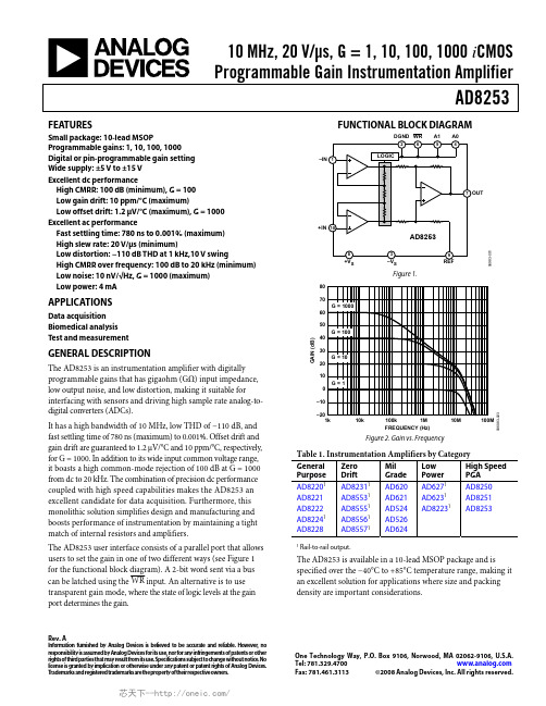
10 MHz, 20 V/μs, G = 1, 10, 100, 1000 i CMOSProgrammable Gain Instrumentation AmplifierAD8253 Rev. AInformation furnished by Analog Devices is believed to be accurate and reliable. However, noresponsibility is assumed by Analog Devices for its use, nor for any infringements of patents or other rights of third parties that may result from its use. Specifications subject to change without notice. No license is granted by implication or otherwise under any patent or patent rights of Analog Devices. T rademarks and registered trademarks are the property of their respective owners. One Technology Way, P.O. Box 9106, Norwood, M A 02062-9106, U.S.A. Tel: 781.329.4700 Fax: 781.461.3113 ©2008 Analog Devices, Inc. All rights reserved.FEATURESSmall package: 10-lead MSOPProgrammable gains: 1, 10, 100, 1000Digital or pin-programmable gain settingWide supply: ±5 V to ±15 VExcellent dc performanceHigh CMRR: 100 dB (minimum), G = 100Low gain drift: 10 ppm/°C (maximum)Low offset drift: 1.2 μV/°C (maximum), G = 1000 Excellent ac performanceFast settling time: 780 ns to 0.001% (maximum)High slew rate: 20 V/μs (minimum)Low distortion: −110 dB THD at 1 kHz,10 V swingHigh CMRR over frequency: 100 dB to 20 kHz (minimum) Low noise: 10 nV/√Hz, G = 1000 (maximum)Low power: 4 mAAPPLICATIONSData acquisitionBiomedical analysisTest and measurementGENERAL DESCRIPTIONThe AD8253 is an instrumentation amplifier with digitally programmable gains that has gigaohm (GΩ) input impedance, low output noise, and low distortion, making it suitable for interfacing with sensors and driving high sample rate analog-to-digital converters (ADCs).It has a high bandwidth of 10 MHz, low THD of −110 dB, and fast settling time of 780 ns (maximum) to 0.001%. Offset drift and gain drift are guaranteed to 1.2 μV/°C and 10 ppm/°C, respectively, for G = 1000. In addition to its wide input common voltage range, it boasts a high common-mode rejection of 100 dB at G = 1000 from dc to 20 kHz. The combination of precision dc performance coupled with high speed capabilities makes the AD8253 an excellent candidate for data acquisition. Furthermore, this monolithic solution simplifies design and manufacturing and boosts performance of instrumentation by maintaining a tight match of internal resistors and amplifiers.The AD8253 user interface consists of a parallel port that allows users to set the gain in one of two different ways (see Figure 1 for the functional block diagram). A 2-bit word sent via a bus can be latched using the WR input. An alternative is to use transparent gain mode, where the state of logic levels at the gain port determines the gain.FUNCTIONAL BLOCK DIAGRAMS S+IN6983-1Figure 1.8070605040302010–10–201k10k100k1M10M100MFREQUENCY (Hz)GAIN(dB)6983-23Figure 2. Gain vs. FrequencyTable 1. Instrumentation Amplifiers by CategoryGeneralPurposeZeroDriftMilGradeLowPowerHigh SpeedPGAAD82201AD82311AD620AD6271AD8250AD8221AD85531AD621AD6231AD8251AD8222AD85551AD524AD82231AD8253AD82241AD85561AD526AD8228AD85571AD6241 Rail-to-rail output.The AD8253 is available in a 10-lead MSOP package and is specified over the −40°C to +85°C temperature range, making it an excellent solution for applications where size and packing density are important considerations.AD8253Rev. A | Page 2 of 24TABLE OF CONTENTSFeatures .............................................................................................. 1 Applications ....................................................................................... 1 General Description ......................................................................... 1 Functional Block Diagram .............................................................. 1 Revision History ............................................................................... 2 Specifications ..................................................................................... 3 Timing Diagram ........................................................................... 5 Absolute Maximum Ratings ............................................................ 6 Maximum Power Dissipation ..................................................... 6 ESD Caution .................................................................................. 6 Pin Configuration and Function Descriptions ............................. 7 Typical Performance Characteristics ............................................. 8 Theory of Operation ...................................................................... 16 Gain Selection ............................................................................. 16 Power Supply Regulation and Bypassing ................................ 18 Input Bias Current Return Path ............................................... 18 Input Protection ......................................................................... 18 Reference Terminal .................................................................... 19 Common-Mode Input Voltage Range ..................................... 19 Layout .......................................................................................... 19 RF Interference ........................................................................... 19 Driving an Analog-to-Digital Converter ................................ 20 Applications Information .............................................................. 21 Differential Output .................................................................... 21 Setting Gains with a Microcontroller ...................................... 21 Data Acquisition ......................................................................... 22 Outline Dimensions ....................................................................... 23 Ordering Guide .. (23)REVISION HISTORY8/08—Rev. 0 to Rev. AChanges to Ordering Guide (23)7/08—Revision 0: Initial VersionAD8253SPECIFICATIONS+V S = +15 V, −V S = −15 V, V REF = 0 V @ T A = 25°C, G = 1, R L = 2 kΩ, unless otherwise noted.Table 2.Parameter Conditions Min Typ Max Unit COMMON-MODE REJECTION RATIO (CMRR)CMRR to 60 Hz with 1 kΩ Source Imbalance +IN = −IN = −10 V to +10 VG = 1 80 100 dBG = 10 96 120 dBG = 100 100 120 dBG = 1000 100 120 dB CMRR to 20 kHz1+IN = −IN = −10 V to +10 VG = 1 80 dBG = 10 96 dBG = 100 100 dBG = 1000 100 dB NOISEVoltage Noise, 1 kHz, RTIG = 1 45 nV/√HzG = 10 12 nV/√HzG = 100 11 nV/√HzG = 1000 10 nV/√Hz0.1 Hz to 10 Hz, RTIG = 1 2.5 μV p-pG = 10 1 μV p-pG = 100 0.5 μV p-pG = 1000 0.5 μV p-p Current Noise, 1 kHz 5 pA/√Hz Current Noise, 0.1 Hz to 10 Hz 60 pA p-p VOLTAGE OFFSETOffset RTI V OS G = 1, 10, 100, 1000 ±150 + 900/G μV Over Temperature T = −40°C to +85°C ±210 + 900/G μV Average TC T = −40°C to +85°C ±1.2 + 5/G μV/°C Offset Referred to the Input vs. Supply (PSR) V S = ±5 V to ±15 V ±5 + 25/G μV/V INPUT CURRENTInput Bias Current 5 50 nA Over Temperature2T = −40°C to +85°C 40 60 nA Average TC T = −40°C to +85°C 400 pA/°C Input Offset Current 5 40 nA Over Temperature T = −40°C to +85°C 40 nA Average TC T = −40°C to +85°C 160 pA/°C DYNAMIC RESPONSESmall-Signal −3 dB BandwidthG = 1 10 MHzG = 10 4 MHzG = 100 550 kHzG = 1000 60 kHz Settling Time 0.01% ΔOUT = 10 V stepG = 1 700 nsG = 10 680 nsG = 100 1.5 μsG = 1000 14 μsRev. A | Page 3 of 24AD8253Rev. A | Page 4 of 24AD8253Rev. A | Page 5 of 24Parameter Conditions Min Typ Max UnitPOWER SUPPLY Operating Range±5 ±15 V Quiescent Current, +I S 4.6 5.3 mA Quiescent Current, −I S 4.5 5.3mA Over Temperature T = −40°C to +85°C 6 mA TEMPERATURE RANGE Specified Performance−40 +85 °C1 See Figure 20 for CMRR vs. frequency for more information on typical performance over frequency.2Input bias current over temperature: minimum at hot and maximum at cold. 3See Figure 30 for input voltage limit vs. supply voltage and temperature. 4See Figure 32, Figure 33, and Figure 34 for output voltage swing vs. supply voltage and temperature for various loads. 5Add time for the output to slew and settle to calculate the total time for a gain change.TIMING DIAGRAMA0, A1WR06983-003Figure 3. Timing Diagram for Latched Gain Mode (See the Timing for Latched Gain Mode Section)AD8253Rev. A | Page 6 of 24ABSOLUTE MAXIMUM RATINGSTable 3.Parameter RatingSupply Voltage ±17 VPower Dissipation See Figure 4Output Short-Circuit CurrentIndefinite 1 Common-Mode Input Voltage ±V S Differential Input Voltage ±V S Digital Logic Inputs±V SStorage Temperature Range –65°C to +125°C Operating Temperature Range 2–40°C to +85°C Lead Temperature (Soldering 10 sec) 300°C Junction Temperature140°C θJA (4-Layer JEDEC Standard Board) 112°C/W Package Glass Transition Temperature140°C1 Assumes the load is referenced to midsupply.2Temperature for specified performance is −40°C to +85°C. For performance to +125°C, see the Typical Performance Characteristics section.Stresses above those listed under Absolute Maximum Ratings may cause permanent damage to the device. This is a stress rating only; functional operation of the device at these or any other conditions above those indicated in the operationalsection of this specification is not implied. Exposure to absolute maximum rating conditions for extended periods may affect device reliability.MAXIMUM POWER DISSIPATIONThe maximum safe power dissipation in the AD8253 package is limited by the associated rise in junction temperature (T J ) on the die. The plastic encapsulating the die locally reaches the junction temperature. At approximately 140°C, which is the glass transition temperature, the plastic changes its properties. Even temporarily exceeding this temperature limit can change the stresses that the package exerts on the die, permanently shifting the parametric performance of the AD8253. Exceeding a junction temperature of 140°C for an extended period can result in changes in silicon devices, potentially causing failure. The still-air thermal properties of the package and PCB (θJA ), the ambient temperature (T A ), and the total power dissipated in the package (P D ) determine the junction temperature of the die. The junction temperature is calculated as()JA D A J θP T T ×+=The power dissipated in the package (P D ) is the sum of the quiescent power dissipation and the power dissipated in the package due to the load drive for all outputs. The quiescent power is the voltage between the supply pins (V S ) times the quiescent current (I S ). Assuming the load (R L ) is referenced tomidsupply, the total drive power is V S /2 × I OUT , some of which isdissipated in the package and some of which is dissipated in theload (V OUT × I OUT ). The difference between the total drive power and the load power is the drive power dissipated in the package.P D = Quiescent Power + (Total Drive Power − Load Power )()L 2OUT L OUTS S S D R V –R V2V I V P ⎟⎟⎠⎞⎜⎜⎝⎛×+×= In single-supply operation with R L referenced to −V S , the worstcase is V OUT = V S /2.Airflow increases heat dissipation, effectively reducing θJA . In addition, more metal directly in contact with the package leads from metal traces through holes, ground, and power planes reduces the θJA .Figure 4 shows the maximum safe power dissipation in the package vs. the ambient temperature on a 4-layer JEDEC standard board.2.001.751.501.251.000.750.500.250–40–20120100806040200M A X I M U M P O W E R D I S S I P A T I O N (W )AMBIENT TEMPERATURE (°C)06983-004Figure 4. Maximum Power Dissipation vs. Ambient TemperatureESD CAUTIONAD8253Rev. A | Page 7 of 24PIN CONFIGURATION AND FUNCTION DESCRIPTIONS–IN DGND –V S A0A1+INREF+V S OUT WRAD8253TOP VIEW(Not to Scale)1234510987606983-005Figure 5. 10-Lead MSOP (RM-10) Pin ConfigurationAD8253Rev. A | Page 8 of 24TYPICAL PERFORMANCE CHARACTERISTICST A @ 25°C, +V S = +15 V , −V S = −15 V , R L = 10 kΩ, unless otherwise noted.CMRR (µV/V)21006983-006N U M B E R O F U N I T S180150120906030–60–40–20020INPUT OFFSET CURRENT (nA)240120180601502109030604020006983-009N U M B E R O F U N I T S–60–20–40Figure 6. Typical Distribution of CMRR, G = 1 Figure 9. Typical Distribution of Input Offset CurrentINPUT OFFSET VOLTAGE, V OSI , RTI (µV)180120150200100006983-007N U M B E R O F U N I T S–200–10006983-0101100kFREQUENCY (Hz)N O I S E (n V /√H z )101001k10k8070605040302010Figure 10. Voltage Spectral Density Noise vs. FrequencyFigure 7. Typical Distribution of Offset Voltage, V OSI 06983-011INPUT BIAS CURRENT (nA)30020025015010050906030006983-008N U M B E R O F U N I T S–90–30–60Figure 11. 0.1 Hz to 10 Hz RTI Voltage Noise, G = 1Figure 8. Typical Distribution of Input Bias CurrentAD8253Rev. A | Page 9 of 2406983-012Figure 12. 0.1 Hz to 10 Hz RTI Voltage Noise, G = 1000 06983-01318011FREQUENCY (Hz)N O I S E (p A /√H z )00k 101001k 10k 161412108642Figure 13. Current Noise Spectral Density vs. Frequency 06983-014Figure 14. 0.1 Hz to 10 Hz Current Noise 201816141210864200.010.1110WARM-UP TIME (Minutes)C H A N G E I N I N P U T O F F S E T V O L T A G E (µV )06983-015Figure 15. Change in Input Offset Voltage vs. Warm-Up Time, G = 10001401201008040600101M06983-016FREQUENCY (Hz)P S R R (d B )1001k 10k 100k 20Figure 16. Positive PSRR vs. Frequency, RTI1401201008040600101M06983-017FREQUENCY (Hz)P S R R (d B )1001k 10k 100k 20Figure 17. Negative PSRR vs. Frequency, RTIAD8253Rev. A | Page 10 of 2420100–10–20–30–40–50–6012.0I B +10.59.07.56.04.53.01.50–15–10–5051015COMMON-MODE VOLTAGE (V)I N P U T B I A S C U R R E N T (n A )I N P U T O F F S E T C U R R E N T (n A )06983-018I B –I OSFigure 18. Input Bias Current and Offset Current vs. Common-Mode Voltage 302520151050–10–5–60–40–20020406080100120140TEMPERATURE (°C)I N P U T B I A S C U R R E N T A N D O F F S E T C U R R E N T (n A )06983-019I B +I B –I OS Figure 19. Input Bias Current and Offset Current vs. Temperature 012010080604020106983-020FREQUENCY (Hz)C M R R (d B )1001k 10k 100k 1MFigure 20. CMRR vs. Frequency120100806040201006983-021FREQUENCY (Hz)C M R R (d B)1001k 10k 100k 1MFigure 21. CMRR vs. Frequency, 1 kΩ Source Imbalance–15–5013006983-022TEMPERATURE (°C)C M R R (µV /V )10155–5–10–30–101030507090110Figure 22. CMRR vs. Temperature, G = 180706050403020100–10–201k10k100k 1M 10M 100MFREQUENCY (Hz)G A I N (d B )006983-023Figure 23. Gain vs. Frequency40302010–10–300–20–40–10–8–6–4–2024681006983-024N O N L I N E A R I T Y (10p p m /D I V )OUTPUT VOLTAGE (V)Figure 24. Gain Nonlinearity, G = 1, R L = 10 kΩ, 2 kΩ, 600 Ω 40302010–10–300–20–40–10–8–6–4–2024681006983-025N O N L I N E A R I T Y (10p p m /D I V )OUTPUT VOLTAGE (V)Figure 25. Gain Nonlinearity, G = 10, R L = 10 kΩ, 2 kΩ, 600 Ω 80604020–20–600–40–80–10–8–6–4–2024681006983-026N O N L I N E A R I T Y (10p p m /D I V )OUTPUT VOLTAGE (V)Figure 26. Gain Nonlinearity, G = 100, R L = 10 kΩ, 2 kΩ, 600 Ω400300200100–100–3000–200–400–10–8–6–4–2024681006983-027N O N L I N E A R I T Y (10 p p m /D I V )OUTPUT VOLTAGE (V)Figure 27. Gain Nonlinearity, G = 1000, R L = 10 kΩ, 2 kΩ, 600 Ω16–1606983-028OUTPUT VOLTAGE (V)I N P U T C O M M O N -M O D E V O L T A G E (V )1284–4–8–12–12–8–44812Figure 28. Input Common-Mode Voltage Range vs. Output Voltage, G = 116–16–161606983-029OUTPUT VOLTAGE (V)I N P U T C O M M O N -M O D E V O L T A G E (V )1284–4–8–12–12–8–44812Figure 29. Input Common-Mode Voltage Range vs. Output Voltage, G = 1000+V S –V S4106983-030SUPPLY VOLTAGE (±V S )I N P U T V O L T A G E (V )R E F E R R E D T O S U P P L Y V O L T A G E S6–1–2+2+168101214Figure 30. Input Voltage Limit vs. Supply Voltage, G = 1, V REF = 0 V, R L = 10 kΩ–1––100m–10–1–100µ–10µ10DIFFERENTIAL INPUT VOLTAGE (V)C U R R E N T (m A )06983-0311001101001Figure 31. Fault Current Draw vs. Input Voltage, G = 1000, R L = 10 kΩ +V S –V S4106983-032SUPPLY VOLTAGE (±V S )OU T P U T V O L T A G E S W I N G (V )R E F E R R E D T O S U P P L Y V O L T A G E S668101214–0.2–0.4–0.6–0.8–1.0–1.2+1.0+1.2+0.8+0.6+0.4+0.2Figure 32. Output Voltage Swing vs. Supply Voltage, G = 1000, R L = 2 kΩ +V S –V S4106983-033SUPPLY VOLTAGE (±V S )O U T P U T V O L T A G E S W I N G (V )R E F E R R E D T O S U P P L Y V O L T A G E S668101214–0.2–0.4–0.6–0.8–1.0+1.0+0.8+0.6+0.4+0.2Figure 33. Output Voltage Swing vs. Supply Voltage, G =1000, R L = 10 kΩ15–1510010k06983-034LOAD RESISTANCE (Ω)1k105–5–10O U T P U T V O L T A G E S W I N G (V )Figure 34. Output Voltage Swing vs. Load Resistance+V S –V S4106983-035OUTPUT CURRENT (mA)668101214–0.4–0.8–1.2–1.6–2.0+2.0+1.6+1.2+0.8+0.4O U T P U T V O L T A G E S W I N G (V )R E F E R R E D T O S U P P L Y V O L T A G E SFigure 35. Output Voltage Swing vs. Output Current06983-036Figure 36. Small-Signal Pulse Response for Various Capacitive Loads, G = 1069TIME (µs)Figure 37. Large-Signal Pulse Response and Settling Time, G = 1, R L= 10 kΩ06983-038TIME (µs)Figure 38. Large-Signal Pulse Response and Settling Time,G = 10, R L= 10 kΩ06983-039TIME (µs)Figure 39. Large-Signal Pulse Response and Settling Time,G = 100, R L= 10 kΩ06983-040TIME (µs)Figure 40. Large-Signal Pulse Response and Settling Time,G = 1000, R L= 10 kΩ06983-041Figure 41. Small-Signal Response,G = 1, R L = 2 kΩ, C L = 10006983-042Figure 42. Small-Signal Response, G = 10, R L = 2 kΩ, C L = 100 pF06983-043Figure 43. Small-Signal Response, G = 100, R L = 2 kΩ, C L = 100 pF06983-044Figure 44. Small-Signal Response, G = 1000, R L = 2 kΩ, C L = 100 pF 06983-045120014000STEP SIZE (V)T I M E (n s )10008006004002004681012141618Figure 45. Settling Time vs. Step Size, G = 1, R L = 10 kΩ06983-04612001400STEP SIZE (V)T I M E (n s )10008006004002004681012141618Figure 46. Settling Time vs. Step Size, G = 10, R L = 10 kΩ06983-04722STEP SIZE (V)T I M E (n s )10008006001800160014004002004681012141618Figure 47. Settling Time vs. Step Size, G = 100, R L = 10 kΩ06983-048STEP SIZE (V)T I M E (µs )1086181614424681012141618Figure 48. Settling Time vs. Step Size, G = 1000, R L = 10 kΩ0–10–20–30–40–50–60–70–80–90–120–110–100101M06983-049FREQUENCY (Hz)T H D + N (d B )1001k 10k 100k Figure 49. Total Harmonic Distortion vs. Frequency,10 Hz to 22 kHz Band-Pass Filter, 2 kΩ Load0–10–20–30–40–50–60–70–80–90–120–110–100101M06983-050FREQUENCY (Hz)T H D + N (d B )1001k 10k 100k Figure 50. Total Harmonic Distortion vs. Frequency, 10 Hz to 500 kHz Band-Pass Filter, 2 kΩ LoadTHEORY OF OPERATIONREFOUTSS 06983-061Figure 51. Simplified SchematicTransparent Gain ModeThe AD8253 is a monolithic instrumentation amplifier based on the classic 3-op-amp topology, as shown in Figure 51. It is fabricated on the Analog Devices, Inc., proprietary i CMOS® process that provides precision linear performance and a robust digital interface. A parallel interface allows users to digitally program gains of 1, 10, 100, and 1000. Gain control is achieved by switching resistors in an internal precision resistor array (as shown in Figure 51).The easiest way to set the gain is to program it directly via a logic high or logic low voltage applied to A0 and A1. Figure 52 shows an example of this gain setting method, referred to through-out the data sheet as transparent gain mode. Tie WR to the negative supply to engage transparent gain mode. In this mode, any change in voltage applied to A0 and A1 from logic low to logic high, or vice versa, immediately results in a gain change. is the truth table for transparent gain mode, and shows the AD8253 configured in transparent gain mode.Table 5Figure 52All internal amplifiers employ distortion cancellation circuitry and achieve high linearity and ultralow THD. Laser-trimmed resistors allow for a maximum gain error of less than 0.03% for G = 1 and a minimum CMRR of 100 dB for G = 1000. A pinout optimized for high CMRR over frequency enables the AD8253 to offer a guaranteed minimum CMRR over frequency of 80 dB at 20 kHz (G = 1). The balanced input reduces the parasitics that in the past had adversely affected CMRR performance.NOTE:1. IN TRANSPARENT GAIN MODE, WR IS TIED TO −V S .THE VOLTAGE LEVELS ON A0 AND A1 DETERMINE THE GAIN. IN THIS EXAMPLE, BOTH A0 AND A1 ARE SET TO LOGIC HIGH, RESULTING IN A GAIN OF 1000.06983-051GAIN SELECTIONThis section describes how to configure the AD8253 for basic operation. Logic low and logic high voltage limits are listed in the Specifications section. Typically, logic low is 0 V and logic high is 5 V; both voltages are measured with respect to DGND. Refer to the specifications table (Table 2) for the permissible voltage range of DGND. The gain of the AD8253 can be set using two methods: transparent gain mode and latched gain mode. Regardless of the mode, pull-up or pull-down resistors should be used to provide a well-defined voltage at the A0 and A1 pins.Figure 52. Transparent Gain Mode, A0 and A1 = High, G = 1000Latched Gain ModeSome applications have multiple programmable devices such as multiplexers or other programmable gain instrumentation amplifiers on the same PCB. In such cases, devices can share a data bus. The gain of the AD8253 can be set using WR as a latch, allowing other devices to share A0 and A1. shows a schematic using this method, known as latched gain mode. The AD8253 is in this mode when Figure 53WR is held at logic high or logic low, typically 5 V and 0 V , respectively. The voltages on A0 and A1 are read on the downward edge of the WR signal as it transitions from logic high to logic low. This latches in the logic levels on A0 and A1, resulting in a gain change. See the truth table listing in for more on these gain changes.Table 6NOTE:FROM LOGIC HIGH TO LOGIC LOW, THE VOLTAGES ON A0AND A1 ARE READ AND LATCHED IN, RESULTING IN AGAIN CHANGE. IN THIS EXAMPLE, THE GAIN SWITCHES TO G = 1000.06983-052Figure 53. Latched Gain Mode, G = 10001X = don’t care.On power-up, the AD8253 defaults to a gain of 1 when inlatched gain mode. In contrast, if the AD8253 is configured in transparent gain mode, it starts at the gain indicated by the voltage levels on A0 and A1 on power-up.Timing for Latched Gain ModeIn latched gain mode, logic levels at A0 and A1 must be held for a minimum setup time, t SU , before the downward edge of WR latches in the gain. Similarly, they must be held for a minimum hold time, t HD , after the downward edge of WR to ensure that the gain is latched in correctly. After t HD , A0 and A1 may change logic levels, but the gain does not change until the next downward edge of WR . The minimum duration that WR can be held high is t -HIGH , and t -LOW is the minimum duration that WR can be held low. Digital timing specifications are listed in The time required for a gain change is dominated by the settling time of the amplifier. A timing diagram is shown in . Table 2.Figure 54When sharing a data bus with other devices, logic levels applied to those devices can potentially feed through to the output of the AD8253. Feedthrough can be minimized by decreasing the edge rate of the logic signals. Furthermore, careful layout of the PCB also reduces coupling between the digital and analog portions of the board.A0, A106983-053Figure 54. Timing Diagram for Latched Gain ModePOWER SUPPLY REGULATION AND BYPASSINGThe AD8253 has high PSRR. However, for optimal performance, a stable dc voltage should be used to power the instrumentation amplifier. Noise on the supply pins can adversely affect per-formance. As in all linear circuits, bypass capacitors must be used to decouple the amplifier.Place a 0.1 μF capacitor close to each supply pin. A 10 μF tantalum capacitor can be used farther away from the part (see Figure 55) and, in most cases, it can be shared by other precision integrated circuits.06983-054Figure 55. Supply Decoupling, REF, and Output Referred to GroundINPUT BIAS CURRENT RETURN PATHThe AD8253 input bias current must have a return path to its local analog ground. When the source, such as a thermocouple, cannot provide a return current path, one should be created (see Figure 56).THERMOCOUPLE+V –V SCAPACITIVELY COUPLED +V SREFCC–V SAD8253TRANSFORMER+V SREF–V SAD8253INCORRECTCAPACITIVELY COUPLEDf HIGH-PASS THERMOCOUPLE+V TRANSFORMER–V SCORRECT06983-055Figure 56. Creating an I BIAS PathINPUT PROTECTIONAll terminals of the AD8253 are protected against ESD. An external resistor should be used in series with each of the inputs to limit current for voltages greater than 0.5 V beyond either supply rail. In such a case, the AD8253 safely handles a continuous 6 mA current at room temperature. For applications where the AD8253 encounters extreme overload voltages, external series resistors and low leakage diode clamps such as BAV199Ls, FJH1100s, or SP720s should be used.REFERENCE TERMINALThe reference terminal, REF, is at one end of a 10 kΩ resistor (see Figure 51). The instrumentation amplifier output is referenced to the voltage on the REF terminal; this is useful when the output signal needs to be offset to voltages other than its local analog ground. For example, a voltage source can be tied to the REF pin to level shift the output so that the AD8253 can interface with a single-supply ADC. The allowable reference voltage range is a function of the gain, common-mode input, and supply voltages. The REF pin should not exceed either +V S or −V S by more than 0.5 V .For best performance, especially in cases where the output is not measured with respect to the REF terminal, source imped-ance to the REF terminal should be kept low because parasiticresistance can adversely affect CMRR and gain accuracy.INCORRECTCORRECT06983-056Figure 57. Driving the Reference PinCOMMON-MODE INPUT VOLTAGE RANGEThe 3-op-amp architecture of the AD8253 applies gain and then removes the common-mode voltage. Therefore, internal nodes in the AD8253 experience a combination of both the gained signal and the common-mode signal. This combined signal can be limited by the voltage supplies even when the individual input and output signals are not. Figure 28 and Figure 29 show the allowable common-mode input voltage ranges for various output voltages, supply voltages, and gains.LAYOUTGroundingIn mixed-signal circuits, low level analog signals need to be isolated from the noisy digital environment. Designing with the AD8253 is no exception. Its supply voltages are referenced to an analog ground. Its digital circuit is referenced to a digital ground. Although it is convenient to tie both grounds to a single ground plane, the current traveling through the ground wires and PC board can cause an error. Therefore, use separate analog and digital ground planes. Only at one point, star ground, should analog and digital ground meet.The output voltage of the AD8253 develops with respect to the potential on the reference terminal. Take care to tie REF to the appropriate local analog ground or to connect it to a voltage that is referenced to the local analog ground.Coupling NoiseTo prevent coupling noise onto the AD8253, follow these guidelines: • Do not run digital lines under the device.• Run the analog ground plane under the AD8253.•Shield fast-switching signals with digital ground to avoid radiating noise to other sections of the board, and never run them near analog signal paths.• Avoid crossover of digital and analog signals.• Connect digital and analog ground at one point only (typically under the ADC).•Power supply lines should use large traces to ensure a low impedance path. Decoupling is necessary; follow the guidelines listed in the Power Supply Regulation and Bypassing section.Common-Mode RejectionThe AD8253 has high CMRR over frequency, giving it greater immunity to disturbances, such as line noise and its associated harmonics, in contrast to typical in amps whose CMRR falls off around 200 Hz. They often need common-mode filters at the inputs to compensate for this shortcoming. The AD8253 is able to reject CMRR over a greater frequency range, reducing the need for input common-mode filtering.Careful board layout maximizes system performance. T o maintain high CMRR over frequency, lay out the input traces symmetrically. Ensure that the traces maintain resistive and capacitive balance; this holds for additional PCB metal layers under the input pins and traces. Source resistance and capacitance should be placed as close to the inputs as possible. Should a trace cross the inputs (from another layer), it should be routed perpendicular to the input traces.RF INTERFERENCERF rectification is often a problem when amplifiers are used in applications where there are strong RF signals. The disturbance can appear as a small dc offset voltage. High frequency signals can be filtered with a low-pass RC network placed at the input of the instrumentation amplifier, as shown in Figure 58. The filter limits the input signal bandwidth according to the following relationship:)C C (R 1FilterFreq C D DIFF +=2π2CCM RC 1FilterFreq π2=where C D ≥ 10 C C .。
三极管的Pspice模型参数详细说明

NK
high-current roll-off coefficient
0.5
NR
reverse current emission coefficient
1.0
NS
substrate p-n emission coefficient
1.0
PTF
excess phase @ 1/(2•TF)Hz
Peak (1, n_occur)
查找第n-occur个峰值点的Y值
Period (1)
计算波形1的周期。
Phase Margin (1,2)
查找波形1在0分贝时波形2的相位。
Pulsewidth (1)
计算波形1的脉冲宽度。
Risetime (1)
计算波形1的上升时间。
Swingr (1, begin-x, end-x)
TRB1
RB temperature coefficient (linear)
0C-1
0.0
RB的温度系数
TRB2
RB temperature coefficient (quadratic)
0C-2
0.0
TRC1
RC temperature coefficient (linear)
0C-1
0.0
TRC2
RC temperature coefficient (quadratic)
0C-2
0.0
TRE1
RE temperature coefficient (linear)
0C-1
0.0
TRE2
RE temperature coefficient (quadratic)
0C-2
多晶硅表面金属杂质的测定方法
多晶硅表面金属杂质的测定方法英文回答:Methods for Determining Metallic Impurities on Polysilicon Surfaces.Metallic impurities on polysilicon surfaces can adversely affect the performance and reliability of photovoltaic cells and other electronic devices. Therefore, it is crucial to accurately determine the presence and concentration of these impurities. Several analytical techniques can be employed for this purpose, each with its own advantages and limitations.Atomic Emission Spectroscopy (AES)。
AES is a surface-sensitive technique that measures the elemental composition of a material by analyzing the emission of light from excited atoms. When a sample is bombarded with an electron beam or other high-energyradiation, atoms in the sample are excited and emit photons of characteristic wavelengths. The intensity of these emitted photons is directly proportional to the concentration of the corresponding elements in the sample. AES can detect metallic impurities on polysilicon surfaces with a detection limit in the range of 10^-10 to 10^-12g/cm2.X-ray Photoelectron Spectroscopy (XPS)。
PCB相关专业术语英汉对照

solder bridge chip load definition deburr foil removal surface smear removal resin-starved area nick mis-picks solderless wrap thermal shock thermal conductivity hot air leveling line HASL heat shield thermal-machanical analysis coefficient of thermal expansion fusing fusing fluid hot strength retention thermal stress method thermal test human resource department emulsion side wetting agent electronic equipment melamine formaldehyde resin heat sink plane SEM strike burned palting cauterization design rule checking RFI elongation bleading production master biological product construction quality wet lamination wet strength retention insulation resistance anter exposure to moisture etching
桥接 切削量 清晰度 去毛刺 去铜箔面 去钻污 缺胶区 缺口 缺纬 绕接 热冲击 热导率 热风整平 热风整平 热隔离 热机分板 热膨胀系数 热熔 热熔液 热态强度保留率 热应力方法 热应力试验 人力资源部 乳胶面 润湿剂 三级封装(各种电子整机产品) 三聚氰胺甲醛树脂 散热层 扫描式电子显微镜 闪镀 烧焦镀层 烧灼 设计规则检查 射频干扰 伸长率 渗出 生产底版 生物制品 施工质量 湿法贴膜 湿强度保留率 湿热后绝缘电阻 蚀刻
- 1、下载文档前请自行甄别文档内容的完整性,平台不提供额外的编辑、内容补充、找答案等附加服务。
- 2、"仅部分预览"的文档,不可在线预览部分如存在完整性等问题,可反馈申请退款(可完整预览的文档不适用该条件!)。
- 3、如文档侵犯您的权益,请联系客服反馈,我们会尽快为您处理(人工客服工作时间:9:00-18:30)。
High-Aspect-Ratio Copper-Via-Filling for Three-Dimensional Chip StackingII.Reduced Electrodeposition Process TimeKazuo Kondo,a,*,z Toshihiro Yonezawa,b Daisuke Mikami,b Toshikazu Okubo,c,*Yuichi Taguchi,d Kenji Takahashi,d and Dale P.Barkey e,*aDepartment of Chemical Engineering,Osaka Prefecture University,1-1,Gakuen-chyo,Sakai,Osaka,599-8531,Japan bDepartment of Applied Chemistry,Okayama University,3-1-1Tushimanaka,Okayama 700-0082,Japan cToppan Printing Company,Limited,Semiconductor Packaging Laboratory,4-2-3,Takanodai-minami,Sugito-Cho,Kita-Katsushika-gun,Saitama 354-8508,Japan dAssociation of Super Advanced Electronic Technologies,Tsukuba Center Incorporated,1-6,Sengen 2-chome,Tsukuba,Ibaraki 305-0047,Japan eDepartment of Chemical Engineering,University of New Hampshire,Durham,New Hampshire 03824,USAThrough-chip electrodes for three-dimensional packaging can offer short interconnection and reduced signal delay.Formation of suitable vias by electrodeposition into cavities presents a filling problem similar to that encountered in the damascene process.Because via dimensions for through-chip filling are larger and have a higher aspect ratio relative to features in damascene,process optimization requires modification of existing superconformal plating baths and plating parameters.In this study,copper filling of high-aspect-ratio through-chip vias was investigated and optimized with respect to plating bath composition and applied current wavetrain.V oid-free vias 70m deep and 10m wide were formed in 60min using additives in combination with pulse-reverse current and dissolved-oxygen enrichment.The effects of reverse current and dissolved oxygen on the performance of superfilling additives is discussed in terms of their effects on formation,destruction,and distribution of a Cu ͑I ͒thiolate accelerant.©2005The Electrochemical Society.͓DOI:10.1149/1.2041047͔All rights reserved.Manuscript submitted February 10,2005;revised manuscript received June 10,2005.Available electronically September 8,2005.Three-dimensional ͑3D ͒chip stacking realizes high-density packaging and high-speed performance.High-aspect-ratio through-chip vias allow short interconnects and reduced signal delays.1-3Copper has been selected as the through-chip electrode because of its compatibility with conventional multilayer interconnection in large-scale integration ͑LSI ͒and back-end processes.A typical 3D packaging process proposed by ASET ͑Association of Super Advanced Electronics Technologies,Japan ͒includes the following steps:͑1͒formation of vias 70m deep by reactive ion etching ͑RIE ͒;͑2͒formation of a SiO 2insulating layer;͑3͒deposi-tion of a TiN barrier layer and a copper seed layer;͑4͒electrodepo-sition of copper inside the via;͑5͒formation of bumps followed by chemical mechanical polishing ͑CMP ͒,polishing,and dicing of the wafer;and ͑6͒multilayer stacking of chips connected through the copper vias.1-3The via width is 10m,and the interconnection pitch is 20m.The minimum wafer thickness is 50m,and a 20m margin is required for polishing the wafer.Hence,a 70m depth is required for the through-chip electrode,and the via aspect ratio is 7.Copper electrodeposition in high-aspect-ratio vias is one of the key technologies for 3D packaging.V oids or seams formed in the via may cause serious problems in reliability.An ASET Electronics SI Report published in 2000͑Ref.4͒cited results of via filling with 10m width and 70m depth.There were voids and seams in the via center.Sasaki et al.5reported fabrication and electronic charac-terization of 3D chip-stacking technologies with through-chip vias 56m deep and 13m in diameter ͑aspect ratio 4.3͒.Unfortu-nately,the details of the electrodeposition process were not reported.In a previous study,6we succeeded in filling 70m vias by opti-mizing the additive composition and applying pulse-reverse current with an applied current density of I on =2.0mA/cm 2.The solution was made up of 130g/L CuSO 4·5H 2O,200g/L H 2SO 4,600ppm polyethylene glycol ͑PEG ͒,100ppm HCl,5ppm bis ͑3-sulfopropyl ͒disulfide ͑SPS ͒,and increasing Janus Green B ͑JGB ͒concentration up to 20to 50mg/L.However,void and seam-free filling required 3.5h.In the 3D packaging process proposed by ASET,RIE and TiN barrier layer formation and copper seed layer formation require about 10min.With a high-speed slurry,the CMP time can also be reduced to about 10min.ASET simulated the process cost of their 3D packaging.If 3.5h were required to fill the via,copper elec-trodeposition would be the rate determining step by a substantial margin,and so reduction of the electrodeposition time is required.The objective of this study was to reduce the electrodeposition time to 1h to make this step compatible with the other operations.ExperimentalThe chip pattern was reported previously.6-10A chip with high-aspect ratio vias ͑70m depth and 10m width ͒was fabricated by a two-stage lithography and etching process,with the overhang re-moved in the second stage.The chip was then mounted on a rotating disk electrode ͑RDE ͒and immersed in the copper plating bath.The RDE rotation speed ͑RDE.;Nikko Keisoku,motor speed controller,SC-5͒was fixed at 1000rpm,and a pulse-reverse current wavetrain ͑Power Supply HB-211and BR-101B,Hokoto Denko ͒was applied.The pulse-reverse wavetrain is defined by three current values,a forward current I on ,a reverse current I rev ,and the off-time current I off =0,and by the corresponding time periods t on ,t rev ,and t off .After deposition,cross sections were cut and carefully polished to expose the via centers.The chip was first embedded in resin and cut with a step cutter ͑MC-170,Marto ͒to within about 100m before the via center.The remaining 100m was then removed by hand polishing,carefully guided by optical microscopy.The cross sections were then examined by field-emission scanning electron microscopy ͑FESEM ͒͑model S-4300,Hitachi ͒.Table I shows the plating-bath composition and pulse-reverse plating conditions.The basic bath consisted of 200g/L CuSO 45H 2O,and 100g/L H 2SO 4.The additives included a proprietary suppressor ͑SPR ͒͑0.5,2,5,or 10mg/L ͒and leveler ͑LEV ͒͑0,0.2,or 0.5mg/L ͒from EEJA ͑Electroplating Engineer of Japan ͒,as well as SPS ͑1,2,or 10mg/L ͒and HCl ͑50,70,or 150mg/L ͒.In a series of experiments at increasing forward current density,begin-*Electrochemical Society Active Member.zE-mail:kkondo@chemeng.osakafu-u.ac.jpJournal of The Electrochemical Society,152͑11͒H173-H177͑2005͒0013-4651/2005/152͑11͒/H173/5/$7.00©The Electrochemical Society,Inc.H173ning with I on=4mA/cm2,the additive compositions and plating conditions were optimized.In the optimization procedure,one vari-able was adjusted at a given applied current until void-freefilling was obtained.The current density was then stepped to a higher value,and a second variable was adjusted until void-freefilling was obtained.The variables were taken in the order:LEV,SPR,HCL, SPS,and H2SO4concentration,followed by the applied current wavetrain and then sparging with oxygen.In the pulse-reverse experiments,forward deposition times T on were100,200,and 300ms.Off times T off were100,150,and200ms.The ratios T on:T rev:T off were held equal to20:1:20.The ratio I rev/I on was held equal to 1.0, 2.0,or 3.0.In the discussion,parameters T on:T rev:T off=200ms:10ms:200ms and I rev/I on=2.0can be as-sumed unless otherwise specified.Sparging with oxygen was in-tended to enrich the solution with dissolved oxygen relative to air-saturated solution.In addition to via-filling experiments,a cyclic voltammetric stripping͑CVS͒method11,12was used to evaluate the inhibition ef-fect of SPR.For these measurements a programmable potentiostat ͑HZ-3000,Hokoto Denko͒and0.2cm2platinum RDE were used.The reference electrode was a saturated calomel electrode͑SCE͒. The potential was scanned between1600and−500mV at a rate of 50mV/s.The copper-stripping charge on the anodic scan was cal-culated from the area under the voltammogram between0.0and 400mV.A normalized charge was defined by dividing the stripping charge at a given SPR concentration by the charge obtained without SPR.Time-potential response curves for direct current,pulse,and pulse reverse were obtained on two kinds of electrodes used to simulate the via outside and the via bottom.The via outside was simulated by a copperfilm electrodeposited on a platinum RDE. This electrode simulates the convective conditions outside of the vias.The via bottom was simulated by a copper electrode patterned with a80m thick dryfilm with50-m-diameter holes.This elec-trode simulates a recessed environment that is shielded from convection.Results and DiscussionOptimization of leveler concentration.—At forward current densities I on up to4mA/cm2,various LEV concentrations were tested in the range of0.0to0.5mg/L.Typical examples of via cross section micrographs are shown in Fig.1for LEV concentra-tions of0.0,0.2,and0.5mg/L,with I on=4mA/cm2and a deposi-tion time of120min.At a LEV concentration of0.0mg/L,there were large voids at the via center,and at0.5mg/L there were small and narrow voids.However,a LEV concentration of0.2mg/L pro-duced no voids,and perfect viafilling was achieved.With the opti-mized LEV concentration of0.2mg/L and applied current density of I on=4mA/cm2,perfect viafilling was achieved in120min.Optimization of suppressor concentration.—The current density was increased to I on=5mA/cm2,and various SPR concentrations in the range of2.0to10.0mg/L were tested.Typical examples of via cross-section micrographs are shown in Fig.2with SPR concen-trations of2.0,5.0,and10.0mg/L for deposition times of90min. SPR concentrations of2.0and10.0mg/L produced small voids at the center,as shown by the arrows.However,a concentration of 5.0mg/L produced no void,and perfect viafilling was achieved. With a SPR concentration of5.0mg/L and applied current density of I on=5mA/cm2,perfect viafilling was achieved in90min. Figure1.Micrographs of via cross sections formed with three different LEVconcentrations.H2SO4,SPR,HCl,and SPS concentration is100g/L,0.5mg/L,70mg/L,and2mg/L,respectively͑a͒0mg/L LEV;͑b͒0.2mg/L LEV;͑c͒0.5mg/L LEV.Figure3.Cyclic voltammetric stripping analysis.The normalized integratedstripping charge is plotted against SPR concentration at RDE rotation speedsof100and1000rpm.Table I.Plating-bath composition and pulse-reverse currentparameters.Basic bath compositionCuSO4·5H2O200g/LH2SO425,50,75,100g/LAdditivesSPR0.5,2,5,10mg/LLEV0,0.2,0.5mg/LHCl50,70,150mg/LSPS͓bis͑3-sulfopropyl͒disulfide͔1,2,10mg/LPulse-reverse conditionsPulse-reverse period T on=100,200,300msReverse current I rev/I on=1.0,2.0,3.0Off time100,150,200msFigure2.Micrographs of via cross sections formed with three different SPRconcentrations.H2SO4,LEV,HCl,and SPS concentration is100g/L,0.2mg/L,70mg/L,and2mg/L,respectively.͑a͒2mg/L SPR;͑b͒5mg/LSPR;͑c͒10mg/L SPR.H174Journal of The Electrochemical Society,152͑11͒H173-H177͑2005͒Optimization of suppressor concentration by cyclic voltammetric stripping analysis .—Figure 3shows the normalized CVS stripping area vs SPR concentration.The RDE rotation speed was 100or 1000rpm.To simulate the outside of the via,where the fluid veloc-ity is relatively high,a rotation speed of 1000rpm was used.To simulate the relatively low fluid velocity inside the via,a rotation speed of 100rpm was used.If the normalized stripping area ͓area/area ͑at SPR =0͔͒is larger for 100rpm than for 1000rpm,deposi-tion is more rapid at the via bottom than the via outside,and bottom-up filling is expected.In Fig.3,the difference in stripping area between 100and 1000rpm is largest at a SPR concentration of 5.0mg/L.This concentration corresponds to prefect via filling as shown in Fig.2.Optimization of HCl,SPS,disulfide,and H 2SO 4concentrations and pulse-reverse current parameters .—In addition to SPR and LEV ,we also optimized the concentrations of HCl,SPS,and H 2SO 4.HCl was varied from 50to 150mg/L,H 2SO 4from 25to 100g/L,and SPS from 1to 10.0mg/L.At this stage,we in-creased the current to I on =6mA/cm 2.Typical examples of via cross section micrographs are shown in Fig.4with 70mg/L HCl,2mg/L SPS,and 25g/L H 2SO 4.Deposition time was 75min.Even at this optimal composition,small voids were formed at the higher current density.With I on =6mA/cm 2,I rev was varied according to I rev /I on =1.0, 2.0,and 3.0.The resulting via cross sections are shown in Fig.5for a deposition time of 75min.With I rev /I on =1.0,I rev is small,the via top was closed,and the deposits had large voids at the center.With I rev /I on =2.0,the void size was smaller.With I rev /I on =3.0,I rev is large and large voids were formed at the via bottom.Oxygen enrichment .—At the optimized additive concentrations and pulse-reverse condition,voids were still produced,and perfect via filling was not obtained at I on =6mA/cm 2͑Fig.4and 5͒.V oid-free filling in 75min was obtained by enrichment of dissolved O 2in the solution.We previously reported the via-bottom acceleration ef-fect of dissolved O 2in through-mask deposition.9Hence,O 2gaswas sparged into the plating solution and a pulse-reverse wavetrain with I on =6mA/cm 2was applied.Figure 6shows micrographs of via cross sections without and with O 2sparging.Without O 2sparg-ing,there is a small void at the via bottom ͑Fig.6a;arrow ͒.How-ever,with O 2sparging there is no void,and perfect via filling is achieved.With O 2gas sparging,perfect via filling without any voids was achieved at I on =6mA/cm 2and a deposition time of 75min,produced no void,and perfect filling was achieved.Two-step electrodeposition process .—The filling time was fi-nally reduced to 60min by application of a two-step deposition process with an initial current density I on =6mA/cm 2for 50min and a second higher current density I on =15mA/cm 2for 10min with O 2gas sparging throughout.Figure 7shows the via cross sec-tion obtained by the two-step process;it produced no void and per-fect filling was achieved.Via cross section shapes with 50min .—The key requirement for perfect via filling is an initial lower current of I on =6mA/cm 2for 50min with O 2gas sparging.Hence,we observed the via cross section with initial lower current of I on =6mA/cm 2for 50min without the second step.Figure 8shows the via cross sections with-out O 2and with O 2.Conformal electrodeposits were formed,and continuous seams from the via bottom to the top remained at the via center without O 2sparging.However,a clear V shape was formed and perfect via filling was achieved without any seam with O 2sparging.Formation of this clear V shape leads to perfect via filling.This bottom-up V-shape formation with O 2is very effective for shortening the electrodeposition time.Mechanism of bottom-up filling with oxygen sparging .—Time-potential curves with O 2and N 2gas sparging are shown in Fig.9.The electrodes are the simulated via outside ͑RDE ͒and via bottom ͑through-mask ͒.A pulse-reverse current wavetrainwasFigure 4.Micrographs of via cross sections formed with optimized HCl,SPS and H 2SO 4concentrations.LEV and SPR concentration is 0.2and 5mg/L,respectively.͑a ͒HCl 70mg/L;͑b ͒SPS 2mg/L;͑c ͒H 2SO 425mg/L.Figure 6.Micrographs of via cross sections formed in the one-stage process with and without O 2enrichment.͑a ͒without O 2enrichment;͑b ͒with O 2enrichment.Figure 5.Micrographs of via cross sections formed with three different pulse-reverse wavetrains.͑a ͒I rev /I on =1.0;͑b ͒I rev /I on =2.0;͑c ͒I rev /I on =3.0.Figure 7.Time shorting with two-step method.͑a ͒Illustration of current change with two-steps method.͑b ͒Cross-sectional micrographs of via.H175Journal of The Electrochemical Society ,152͑11͒H173-H177͑2005͒applied.With O 2gas sparging,the simulated via outside is at a more negative potential,and hence more inhibited than under N 2sparging.However,no potential difference is observed for the simulated via bottom under O 2or N 2sparging.In equilibrium with the metal,copper plating solutions contain a cuprous ion concentration in the millimolar range.Dissolved oxygen consumes the cuprous ion and removes the solution from equilibrium.13,14Formation reactions of Cu ͑I ͒thiolate accelerator and oxidation reaction of Cu +to Cu ++are shown below 152Cu 2++4MPS →2Cu ͑͒thiolate +SPS +4H +͓1͔2Cu ++1/2O 2+2H +→2Cu 2++H 2O͓2͔The distribution of these reactions in and around the via is illustrated in Fig.10.The outside of the via is more accessible to dissolved oxygen than the via bottom,since the chip is rotated at 1000rpm.The Cu ͑I ͒thiolate accelerant is thus readily oxidized to Cu 2+at the via outside ͑Eq.2͒.Deep inside the via,transport of dissolved O 2is impeded and accumulation of Cu ͑I ͒thiolate occurs.Hence,the Cu ͑I ͒thiolate is depleted at the via outside relative to the via bottom,and deposition is more inhibited there.Figure 10illustrates the mechanism of the bottom-up via filling with O 2sparging.Depletion of Cu ͑I ͒thiolate occurs at the via outside and accumulation of Cu ͑I ͒thiolate occurs at the via bottom.This inhibition and accelera-tion by Cu ͑I ͒thiolate accumulation results in the marked V-shaped via cross section observed in Fig.8b.ConclusionsV oid-free filling of 70m deep and 10m wide vias was achieved by copper deposition with optimized additive concentra-tions,a pulse-reverse wavetrain,oxygen enrichment,and a two-stage process.Optimized proprietary additive concentrations of5mg/L SPR and 0.2mg/L LEV produced void-free filling at 5mA/cm 2with a filling time of 90min.The difference in normal-ized stripping area ͓Ar/Ar ͑SPR =0͔͒detected by CVS at RDE ro-tation speeds of 100and 1000rpm shows the largest value at the optimum SPR concentration of 5mg/L.SPS,HCl,and H 2SO 4con-centrations were optimized at a current density of I on =6mA/cm 2.The optimized concentrations are 2mg/L SPS,70mg/L HCl,and 25g/L H 2SO 4.The optimized pulse-reverse conditions were T on :T rev :T off =200ms:10ms:200ms and I rev /I on =2.0.However,at this composition small voids always formed at a current density of I on =6mA/cm 2.Perfect via filling was obtained with the optimized plating bath with I on =6mA/cm 2and 75min by sparging with O 2.The effect of O 2gas is interpreted to result from oxidation of a Cu ͑I ͒thiolate accelerant preferentially at the outside of the vias.Fi-nally,a two-step electrodeposition process consisting of initial lower current of I on =6mA/cm 2for 50min and second higher current of I on =15mA/cm 2for 10min was applied,resulting in perfect via filling within 60min.A clear,bottom-up V-shape-formed via cross section was observed after the initial lower current of I on =6mA/cm 2.AcknowledgmentsThis work was supported by NEDO ͑New Energy Development Organization ͒as a part of the project of “Research and Development of Ultrahigh-Density Electronics System Integration Technology.”Thanks to EEJA Electroplating Engineers of Japan for supplying us with the additives.Osaka Prefecture University assisted in meeting the publication costs of this article.References1.M.Koyanagi,T.Nakamura,K.W.Lee,Y .Igarashi,T.Mizukusa,Y .Yamada,T.Morooka,and H.Kurino,in Advanced Metallization Conference 2001(AMC 2001),A.J.McKerrow,Y .Shacham-Diamond,S.Zaima,and T.Ohba,Editors,Conference Proceedings ULSI XVIII,p.20,The Materials Research Society,War-rendale,PA ͑2001͒.2.M.Tomisaka,H.Yonemura,M.Hoshino,and K.Takahashi,in Solid State Devices and Materials ,p.40,The Japan Society of Applied Physics,Tokyo ͑2001͒.3.K.Takahashi,in The 2nd Annual Meeting on Electronic SI Technologies ,p.43,Tokyo ͑2001͒͑in Japanese ͒.4.K.Takahashi,in The 1st Annual Meeting on Electronic SI Technologies,p.23,Tokyo ͑2000͒͑in Japanese ͒.5.T.Harada,K.Asao,K.Sasaki,and Y .Kami,in 2001ICEP Proceedings ,p.39,Tokyo ͑2001͒.6.J.Sun,K.Kondo,T.Okamura,S.Oh,M.Tomisaka,H.Yonemura,and M.Hoshino,J.Electrochem.Soc.,150,G355͑2003͒.7.S.Oh,T.Yonezawa,K.Kondo,M.Tomisaka,H.Yonemura,M.Hoshino,Y .Taguchi,and K.Takahashi,in 2003ICEP Proceedings ,p.244,Tokyo ͑2003͒.Figure 8.Micrographs of via cross sections formed in the two-stage process with and without O 2enrichment.͑a ͒without O 2enrichment;͑b ͒with O 2enrichment.Figure 9.Chronopotentiometric curves taken under N 2sparging and under O 2sparging.Figure 10.Mechanism of bottom-up via filling with O 2enrichment.Cu ͑I ͒is generated at the metal surface by proportionation.It is consumed in solution by reaction with oxygen.Outside the via,consumption of Cu ͑I ͒is favored by comparatively rapid transport of dissolved oxygen in the convective regime.Inside the via,transport of dissolved O 2is impeded and accumulation of Cu ͑I ͒thiolate occurs.The result is accumulation of Cu ͑I ͒thiolate accelerant inside the via and its depletion outside the via.H176Journal of The Electrochemical Society ,152͑11͒H173-H177͑2005͒8.K.Kondo,T.Okamura,S.Oh,Y.Yonezawa,M.Tomisaka,H.Yonemura,M.Hoshino,Y.Taguchi,and K.Takahashi,J.Jap.Inst.Electronics Packaging,6,596͑2003͒.9. D.P.Barkey,K.Kondo,T.Matsumoto,and A.Wu,Abstract189f,AICHE Meet-ing,San Francisco͑2003͒.10.K.Kondo,T.Matsumoto,and K.Watanabe,J.Electrochem.Soc.,151,C250͑2004͒.11. D.Tench and C.Ogden,J.Electrochem.Soc.,125,194͑1978͒.12.P.Taephaisitphonge,Y.Cao,and A.C.West,J.Electrochem.Soc.,148,C492͑2001͒.13. D.P.Barkey,F.Oberholtzer,and Q.Wu,J.Electrochem.Soc.,145,590͑1998͒.14. D.Hua and D.Barkey,Plat.Surf.Finish.,90,40͑2003͒.15. E.Farndon,F.C.Walsh,and S.A.Campbell,J.Appl.Electrochem.,25,572͑1995͒.H177Journal of The Electrochemical Society,152͑11͒H173-H177͑2005͒。