2SC2630中文资料
2SC6082;中文规格书,Datasheet资料
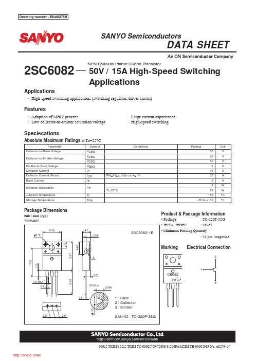
No. A0279-1/7Applications • High-speed switching applications (switching regulator, driver circuit)Features• Adoption of MBIT process•Large current capacitance • Low collector-to-emitter saturation voltage • High-speed switchingSpeci fi cationsAbsolute Maximum Ratingsat Ta=25°CParameterSymbol ConditionsRatingsUnit Collector-to-Base Voltage V CBO60V Collector-to-Emitter Voltage V CES 60V V CEO 50V Emitter-to-Base Voltage V EBO 6V Collector Current I C 15A Collector Current (Pulse)I CP PW ≤10μs, duty cycle ≤1%20A Base Current I B 3A Collector Dissipation P C 2W Tc=25°C23W Junction Temperature Tj 150°C Storage TemperatureTstg--55 to +150°CPackage Dimensionsunit : mm (typ)7529-00260612 TKIM/12512 TKIM TC-00002709/72606/31506FA MSIM TB-000020892SC6082NPN Epitaxial Planar Silicon Transistor50V / 15A High-Speed Switching ApplicationsProduct & Package Information• Package : TO-220F-3SG • JEITA, JEDEC : SC-67• Minimum Packing Quantity : 50 pcs./magazineMarkingElectrical ConnectionC6082LOT No.Electrical Characteristicsat Ta=25°CParameterSymbol ConditionsRatingsUnit mintypmaxCollector Cutoff Current I CBO V CB =40V , I E =0A 10μA Emitter Cutoff Current I EBO V EB =4V , I C =0A 10μADC Current Gain h FE 1V CE =2V , I C =330mA 200560h FE 2V CE =2V , I C =10A 50Gain-Bandwidth Product f T V CE =10V , I C=2A195MHz Output CapacitanceCob V CB =10V , f=1MHz 85pF Collector-to-Emitter Saturation Voltage V CE (sat)I C =7.5A, I B =375mA 200400mV Base-to-Emitter Saturation Voltage V BE (sat)I C =7.5A, I B =375mA 1.2V Collector-to-Base Breakdown Voltage V (BR)CBO I C =100μA, I E =0A 60V Collector-to-Emitter Breakdown Voltage V (BR)CES I C =100μA, R BE =0Ω60V V (BR)CEO I C =1mA, R BE =∞50V Emitter-to-Base Breakdown Voltage V (BR)EBO I E =100μA, I C =0A 6V Turn-On Time t on See speci fi ed Test Circuit52ns Storage Time t stg 560ns Fall Timet f37nsSwitching Time Test CircuitOrdering InformationDevicePackage Shippingmemo2SC6082-1ETO-220F-3SG50pcs./magazine Pb FreeCC I C =20I B1= --20I B2=5APW=20μsD.C.≤1%Collector-to-Emitter V oltage, V CE -- VC o l l e c t o r C u r r e n t , I C -- ACollector-to-Emitter V oltage, V CE -- VC o l l e c t o r C u r r e n t , I C -- AIT10574IT105751001000100.010.11.0100.010.11.010100100010100100010100100010Collector Current, I C -- AD C C u r r e n t G a i n , h F ECollector Current, I C-- AD C C u r r e n t G a i n , h F EBase-to-Emitter V oltage, V BE -- VC o l l e c t o r C u r r e n t , I C -- ACollector-to-Base V oltage, V CB -- VO u t p u t C a p a c i t a n c e , C o b -- p FCollector Current, I C -- AC o l l e c t o r -t o -E m i t t e r S a t u r a t i o n V o l t a g e , V C E (s a t ) -- VG a i n -B a n d w i d t h P r o d u c t , f T -- M H zCollector Current, I C -- AIT10576IT10577IT10578IT10581IT105800.10.01IT10579C o l l e c t o r -t o -E m i t t e r S a t u r a t i o n V o l t a g e , V C E (s a t ) -- VCollector Current, I C -- ACollector Current, I C -- AB a s e -t o -E m i t t e r S a t u r a t i o n V o l t a g e , V B E (s a t ) -- VIT10582321.02375IT105830.10.01Collector-to-Emitter V oltage, V CE -- VC o l l e c t o r C u r r e n t , I C -- AAmbient Temperature, Ta -- °CC o l l e c t o rD i s s i p a t i o n , P C -- WCase Temperature, Tc -- °CC o l l e c t o rD i s s i p a t i o n , P C -- WIT167110.010.11.010100IT16709IT16710Magazine Specifi cation 2SC6082-1EOutline Drawing2SC6082-1EMass (g)Unit1.8mm* For referenceThis catalog provides information as of June, 2012. Specifi cations and information herein are subject to change without notice.分销商库存信息: ONSEMI2SC6082。
电子电气必备常识
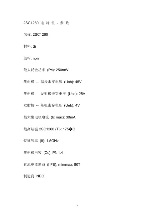
2SC1260 电特性- 参数名称: 2SC1260材料: Si结构: npn最大耗散功率(Pc): 250mW集电极-- 基极击穿电压(Ucb): 45V 集电极-- 发射极击穿电压(Uce): 25V 发射极-- 基极击穿电压(Ueb): 4V最大集电极电流(Ic max): 30mA最高结温 2SC1260 (Tj): 175�C特征频率(ft): 1.5GHz集电极电容(Cc), Pf: 1.4直流电流增益(hFE), min/max: 80T制造商: NEC1.共射极电路当信号与基极偏压同相时,基极电位升高,使基极电流增大,集电极电位降低,集电极负载电流会比基极电流增大量成倍增大;当信号与基极偏压反相时,基极电位降低,使基极电流减小,集电极电位升高,集电极负载电流会比基极电流减小量成倍减小。
集电极电流变化量与三极管放大倍数有关。
共射极电路集电极电位变化方向与基极电位变化方向相反,因此也叫反相器。
信号电流不是直接穿过三极管,只能在基极回路流通,在集电极回路可得到放大的电流信号,这两个回路的公共点是发射极,因此又叫共发射极电路。
共射极电路又称反相放大电路,其特点为电压增益大,输出电压与输入电压反相,低频性能差,适用于低频、和多级放大电路的中间级。
2.共集电极电路共集电极电路又称射极输出器、电压跟随器,其特点是:电压增益小于1而又近似等于1,输出电压与输入电压同相,输入电阻高,输出电阻低,常用于多级放大电路的输入级、输出级或缓冲级。
3 .共基极电路电路特点:输出电压与输入电压同相,输入电阻底,输出电阻高,常用于高频或宽频带电路。
4.反馈是将输出信号的一部分或全部以通过反馈网络送到输入端。
负反馈放大电路有四种不同类型,由瞬时极性判断反馈的性质,由输出端判别电压或电流反馈,由输入端判别串联或并联反馈。
去耦电容在电子电路中,去耦电容和旁路电容都是起到抗干扰的作用,电容所处的位置不同,称呼就不一样了。
2SC4250中文资料(toshiba)中文数据手册「EasyDatasheet - 矽搜」

反向传输电容 过渡频率 转换增益 噪声系数
(Ta = 25°C)
符号
测试条件
ICBO IEBO V (BR) CEO hFE Cre
fT Gce NF
VCB = 25 V, I E = 0 VEB = 3 V, I C = 0 IC = 1毫安,我B = 0 VCE = 10 V, I C = 5毫安 VCB = 10 V, I E = 0, f = 1兆赫 VCE = 10 V, I C = 5毫安 VCC = 12 V, f = 200兆赫,女 L = 260兆赫 (图1)
• 请联系您的东芝销售代表了解详细信息,以环境问题,如产品的RoHS指令的兼容性. 请遵守产品使用与规范纳入或使用受控物质,包括但不限于,欧盟RoHS指令的所有适用的法律和法规.东芝对发生违规作为适用的法律和法规而导致的损害 或损失不承担任何责任.
5
2007-11-01
• 东芝公司及其子公司和附属公司(统称为“TOSHIBA”),保留这份文件中更改信息的权利,以及相关的硬件,软件和系统(统称为“产品”),恕不另行通 知.
• 本文档以及任何信息均不得转载未经东芝事先书面许可.即使 东芝的书面许可,复制是允许的,只要在没有任何改动/遗漏.
• 虽然东芝的作品不断地提高产品的质量和可靠性,产品会发生故障或失败.客户 负责符合安全标准和用于提供充分的设计和保障其硬件,软件和 这最大限度地降低风险,并避免出现在产品的故障或失效可能导致生命丧失,身体系统 人身伤害或财产损失,包括数据丢失或损坏.在创作和制作的设计和使用,客户必须 也指,符合(一)中的所有相关信息,东芝的最新版本,包括但不限于本文件, 规格,数据表和应用笔记产品的注意事项和条件中规定的“TOSHIBA 半导体可靠性手册“和(b)对于该产品将与或使用的应用程序的说明.客户全权负责自己的产品设计或应用程序的各个方面,包括但不限于:(a)确定 的利用这样的设计或应用该产品的适当性; (b)评价和确定本文档中包含的任何信息的适用性,或图表,图表,程序,算法,示例应用电路,或 任何其他引用文件; (三)验证这样的设计和应用的所有运行参数.
2SC5570资料
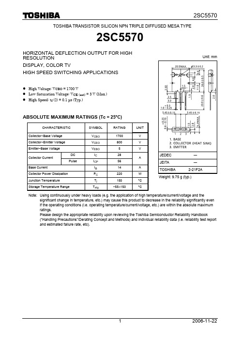
TOSHIBA TRANSISTOR SILICON NPN TRIPLE DIFFUSED MESA TYPE2SC5570HORIZONTAL DEFLECTION OUTPUT FOR HIGH RESOLUTIONDISPLAY, COLOR TVHIGH SPEED SWITCHING APPLICATIONSz High Voltage: V CBO = 1700 Vz Low Saturation Voltage: V CE (sat) = 3 V (Max.) z High Speed: t f (2) = 0.1 μs (Typ.)ABSOLUTE MAXIMUM RATINGS (Tc = 25°C)CHARACTERISTIC SYMBOL RATING UNITCollector −Base Voltage V CBO 1700 V Collector −Emitter Voltage V CEO 800 V Emitter −Base Voltage V EBO5 V DC I C 28 Collector Current PulseI CP 56ABase CurrentI B 14 A Collector Power Dissipation P C 220 W Junction Temperature T j 150 °C Storage Temperature RangeT stg−55~150 °CNote: Using continuously under heavy loads (e.g. the application of high temperature/current/voltage and thesignificant change in temperature, etc.) may cause this product to decrease in the reliability significantly even if the operating conditions (i.e. operating temperature/current/voltage, etc.) are within the absolute maximum ratings.Please design the appropriate reliability upon reviewing the Toshiba Semiconductor Reliability Handbook(“Handling Precautions”/Derating Concept and Methods) and individual reliability data (i.e. reliability test report and estimated failure rate, etc).Unit: mmJEDEC ― JEITA―TOSHIBA 2-21F2A Weight: 9.75 g (typ.)ELECTRICAL CHARACTERISTICS (Tc = 25°C)CHARACTERISTIC SYMBOL TEST CONDITION MIN TYP. MAX UNITCollector Cut −off Current I CBO V CB = 1700 V, I E = 0 ―― 1 mA Emitter Cut −off CurrentI EBO V EB = 5 V, I C = 0 ― ― 100μAEmitter −Base Breakdown VoltageV (BR) CEO I C = 10 mA, I B = 0 800 ―― Vh FE (1)V CE = 5 V, I C = 2 A 22 ― 48 h FE (2) V CE = 5 V, I C = 8 A 12.5 ― 25 DC Current Gainh FE (3)V CE = 5 V, I C = 22 A 4.5 ― 7.5 ― Collector −Emitter Saturation Voltage V CE (sat) I C = 22 A, I B = 5.5 A ―― 3 VBase −Emitter Saturation Voltage V BE (sat) I C = 22 A, I B = 5.5 A ― 1.0 1.5 V Transition Frequency f T V CE = 10 V, I C = 0.1 A ― 2 ― MHz Collector Output CapacitanceC ob V CB = 10 V, I E = 0, f = 1 MHz ― 470 ― pF Storage Timet stg (1) ― 2.6 3.0Fall Time t f (1) I CP = 10 A, I B1 (end) = 1.4 Af H = 64 kHz― 0.2 0.3 μsStorage Time t stg (2) ― 1.4 1.6Switching TimeFall Timet f (2)I CP = 8 A, I B1 (end) = 1.2 A f H = 130 kHz― 0.10 0.15μsMarkinglead (Pb)-free finish.RESTRICTIONS ON PRODUCT USE20070701-EN •The information contained herein is subject to change without notice.•TOSHIBA is continually working to improve the quality and reliability of its products. Nevertheless, semiconductor devices in general can malfunction or fail due to their inherent electrical sensitivity and vulnerability to physical stress. It is the responsibility of the buyer, when utilizing TOSHIBA products, to comply with the standards of safety in making a safe design for the entire system, and to avoid situations in which a malfunction or failure of such TOSHIBA products could cause loss of human life, bodily injury or damage to property.In developing your designs, please ensure that TOSHIBA products are used within specified operating ranges as set forth in the most recent TOSHIBA products specifications. Also, please keep in mind the precautions and conditions set forth in the “Handling Guide for Semiconductor Devices,” or “TOSHIBA Semiconductor Reliability Handbook” etc.• The TOSHIBA products listed in this document are intended for usage in general electronics applications (computer, personal equipment, office equipment, measuring equipment, industrial robotics, domestic appliances, etc.).These TOSHIBA products are neither intended nor warranted for usage in equipment that requires extraordinarily high quality and/or reliability or a malfunction or failure of which may cause loss of human life or bodily injury (“Unintended Usage”). Unintended Usage include atomic energy control instruments, airplane or spaceship instruments, transportation instruments, traffic signal instruments, combustion control instruments, medical instruments, all types of safety devices, etc.. Unintended Usage of TOSHIBA products listed in his document shall be made at the customer’s own risk.•The products described in this document shall not be used or embedded to any downstream products of which manufacture, use and/or sale are prohibited under any applicable laws and regulations.• The information contained herein is presented only as a guide for the applications of our products. No responsibility is assumed by TOSHIBA for any infringements of patents or other rights of the third parties which may result from its use. No license is granted by implication or otherwise under any patents or other rights of TOSHIBA or the third parties.• Please contact your sales representative for product-by-product details in this document regarding RoHS compatibility. Please use these products in this document in compliance with all applicable laws and regulations that regulate the inclusion or use of controlled substances. Toshiba assumes no liability for damage or losses occurring as a result of noncompliance with applicable laws and regulations.。
2SC2632中文资料

hFE — IC
600 VCE=10V 300
fT — I E
Collector output capacitance Cob (pF)
VCB=10V f=100MHz Ta=25˚C 5
Cob — VCB
IE=0 f=1MHz Ta=25˚C 4
Forward current transfer ratio hFE
R 130 ~ 220 S 185 ~ 330 hFE
Rank
1
元器件交易网
Transistor
PC — Ta
1.2 120 VCE=10V 25˚C
2SC2632
IC — VBE
Collector to emitter saturation voltage VCE(sat) (V)
(Ta=25˚C)
Ratings 150 150 5 100 50 1 150 –55 ~ +150 Unit V V V mA mA W ˚C ˚C
0.45–0.1 1.27 1.27
+0.2
13.5±0.5
0.7–0.2
+0.3
Satisfactory linearity of forward current transfer ratio hFE. High collector to emitter voltage VCEO. Small collector output capacitance Cob.
(Ta=25˚C)
Symbol ICBO VCEO VEBO hFE fT Cob NV
*
Conditions VCB = 100V, IE = 0 IC = 0.1mA, IB = 0 IE = 10µA, IC = 0 VCE = 5V, IC = 10mA IC = 30mA, IB = 3mA VCB = 10V, IE = –10mA, f = 200MHz VCB = 10V, IE = 0, f = 1MHz VCE = 10V, IC = 1mA, GV = 80dB Rg = 100kΩ, Function = FLAT
2SC3306中文资料(Inchange Semiconductor)中文数据手册「EasyDatasheet - 矽搜」
VCEsat VBEsat
集电极 - 发射极饱和电压
基地发射极饱和电压
ICBO I EBO hFE
开关时间
集电极截止电流 发射极截止电流
DC电流增益
tr
上升时间
t stg
贮存时间
tf
下降时间
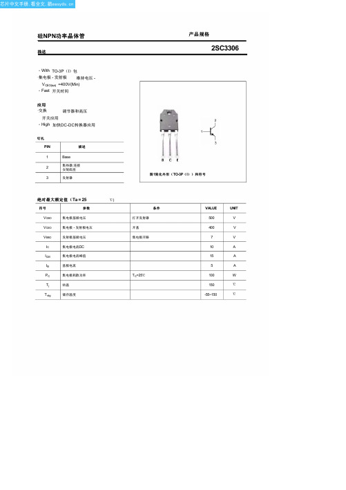
产品规格
2SC3306
条件
IC=10毫安,I B=0 IC= 1mA时E,I=0 IE= 1mA时,CI=0 IC=5A; I B=0.5A IC=5A; I B=0.5A VCB=400V; I E=0 VEB=7V; I C=0 IC=5A ; V CE=5V
TC=25℃
VALUE
UNIT
500ห้องสมุดไป่ตู้
V
400
V
7
V
10
A
15
A
5
A
100
W
150
℃
-55~150
℃
芯片中文手册,看全文,戳
硅NPN功率晶体管
特性 除非另有说明 TJ = 25℃
符号
参数
V(BR)CEO 集电极 - 发射极击穿电压 V(BR)CBO 集电极基击穿电压 V(BR)EBO 发射基地击穿电压
安装底座 发射器
产品规格
2SC3306
图 1简化外形( TO-3P( I))和符号
绝对最大额定值(Ta = 25
℃)
符号
参数
VCBO
集电极基极电压
VCEO
集电极 - 发射极电压
VEBO
发射极基极电压
IC
集电极电流DC
ICM
集电极电流峰值
IB
基极电流
PC
集电极耗散功率
三极管2SC
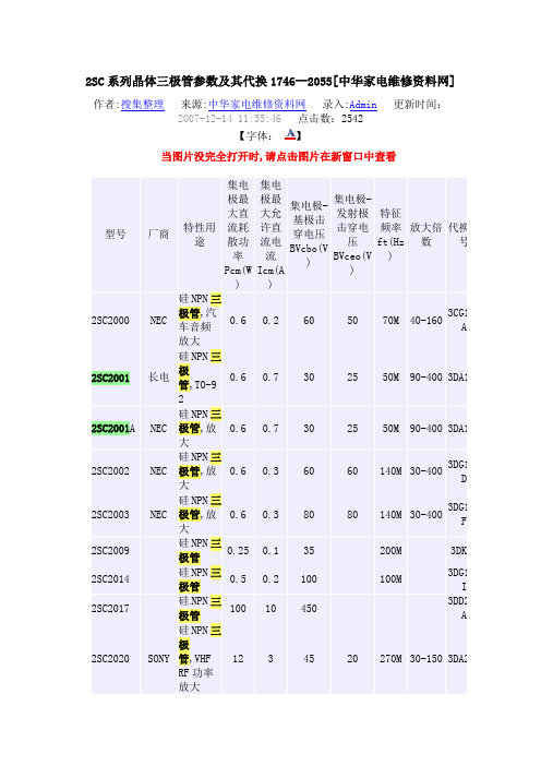
2SC系列晶体三极管参数及其代换1746--2055[中华家电维修资料网]作者:搜集整理来源:中华家电维修资料网录入:Admin更新时间:2007-12-1411:55:46点击数:2542【字体:】当图片没完全打开时,请点击图片在新窗口中查看型号厂商特性用途集电极最大直流耗散功率Pcm(W)集电极最大允许直流电流Icm(A)集电极-基极击穿电压BVcbo(V)集电极-发射极击穿电压BVceo(V)特征频率ft(Hz)放大倍数代换型号2SC2000 NEC 硅NPN三极管,汽车音频放大0.6 0.2 60 50 70M 40-1603CG180A2SC2001长电硅NPN三极管,TO-920.6 0.7 30 25 50M 90-400 3DA18A2SC2001A NEC 硅NPN三极管,放大0.6 0.7 30 25 50M 90-400 3DA18A2SC2002 NEC 硅NPN三极管,放大0.6 0.3 60 60 140M 30-4003DG130D2SC2003 NEC 硅NPN三极管,放大0.6 0.3 80 80 140M 30-4003DG182F2SC2009 硅NPN三极管0.25 0.1 35 200M 3DK2A2SC2014 硅NPN三极管0.5 0.2 100 100M3DG180I2SC2017 硅NPN三极管100 10 4503DD264A2SC2020 SONY 硅NPN三极管,VHFRF功率放大12 3 45 20 270M 30-150 3DA22A2SC2021ROHM极管,一般小信号放大,配对管2SA937 0.3 0.1 50 40 180M120-8202SC2021L N 硅NPN 三极管,低噪声 0.3 0.15 50 180-5602SC2022硅NPN 三极管 30130010M3DK205F 2SC2023SANKEN 硅NPN 三极管,串联调整,开关,一般放大 40 2 300 300 10M 303DK206F2SC2024硅NPN 三极管 1 1 80 150M 3DK30C2SC2025NEC硅NPN 中功率UHF-VHF 三极管 0.25 0.07 25 12 4.5G 20-2502SC2026NEC 硅NPN 三极管,VHF ,UHF 低噪声放大 0.25 0.05 30 14 2G 25-200 3DG44C2SC2027硅NPN 三极管 50 5 1500 3DA58I2SC2028 FUJI 硅NPN 三极管,高频放大 5 1.5 80 50 250M 90-320 3DA14B 2SC2029硅NPN 三极管 10280 150M 3DK104E 2SC203硅NPN 三极管 0.35 0.2 40 350M3DG130C2SC2034 TOSHIBA硅NPN 三极管,功率放大 12 2 120 90 150M 50-200 2SC2035硅NPN 三极管0.3 0.3 50 350M 3DK29B2SC2036TOSHIB A 资料来自网上118080150M100整理,硅NPN,功率放大2SC2037 NEC 一般NPN晶体管0.25 0.07 25 12 4.5G 20-2502SC2039 硅NPN三极管80 8 70 200M 3DA73B2SC204 硅NPN三极管0.35 0.2 20 350M3DG130C2SC2043 FUJI 硅NPN三极管,功率放大25 8 70 70 220M 20-2002SC2050 FUJI 硅NPN三极管,功率放大13 8 70 70 150M 20-1502SC2053 MIT 硅NPN三极管,VHFRF放大0.6 0.3 40 17 10-1802SC2055 MIT 硅NPN三极管,VHFRF放大0.5 0.3 18 9 1.7G 10-1803DG130A。
2SC2620中文资料

2SC2620Silicon NPN Epitaxial PlanarApplicationVHF amplifier, Local oscillatorOutline2SC26202Absolute Maximum Ratings (Ta = 25°C)ItemSymbol Ratings Unit Collector to base voltage V CBO 30V Collector to emitter voltage V CEO 20V Emitter to base voltage V EBO 4V Collector currentI C 20mA Collector power dissipation P C 100mW Junction temperature Tj 150°C Storage temperatureTstg–55 to +150°CElectrical Characteristics (Ta = 25°C)ItemSymbol Min Typ Max Unit Test conditions Collector to base breakdown voltageV (BR)CBO30——V I C = 10 µA, I E = 0Collector to emitter breakdown voltageV (BR)CEO 20——V I C = 1 mA, R BE = ∞Emitter to base breakdown voltageV (BR)EBO 4——V I E = 10 µA, I C = 0Collector cutoff current I CBO ——0.5µA V CB = 10 V, I C = 0Emitter cutoff current I EBO ——0.5µAV EB = 2 V, I C = 0DC current transfer ratio h FE *160—200V CE = 6 V, I C = 1 mA Collector to emitter saturation voltageV CE(sat)—0.17—V I C = 20 mA, I B = 4 mA Base to emitter voltage V BE —0.72—V V CE = 6 mA, I C = 1 mA Gain bandwidth product f T —940—MHz V CE = 6 V, I C = 5 mA Collector output capacitance Cob—0.9—pF V CB = 10 V, I E = 0, f = 1 MHzNote: 1.The 2SC2620 is grouped by h FE as follows.Grade B C Mark QB QC h FE60 to 120100 to 200See characteristic curves of 2SC535.2SC26203Hitachi CodeJEDECEIAJWeight (reference value)MPAK—Conforms0.011 gUnit: mm元器件交易网Cautions1.Hitachi neither warrants nor grants licenses of any rights of Hitachi’s or any third party’s patent,copyright, trademark, or other intellectual property rights for information contained in this document.Hitachi bears no responsibility for problems that may arise with third party’s rights, includingintellectual property rights, in connection with use of the information contained in this document.2.Products and product specifications may be subject to change without notice. Confirm that you have received the latest product standards or specifications before final design, purchase or use.3.Hitachi makes every attempt to ensure that its products are of high quality and reliability. However,contact Hitachi’s sales office before using the product in an application that demands especially high quality and reliability or where its failure or malfunction may directly threaten human life or cause risk of bodily injury, such as aerospace, aeronautics, nuclear power, combustion control, transportation,traffic, safety equipment or medical equipment for life support.4.Design your application so that the product is used within the ranges guaranteed by Hitachi particularly for maximum rating, operating supply voltage range, heat radiation characteristics, installationconditions and other characteristics. Hitachi bears no responsibility for failure or damage when used beyond the guaranteed ranges. Even within the guaranteed ranges, consider normally foreseeable failure rates or failure modes in semiconductor devices and employ systemic measures such as fail-safes, so that the equipment incorporating Hitachi product does not cause bodily injury, fire or other consequential damage due to operation of the Hitachi product.5.This product is not designed to be radiation resistant.6.No one is permitted to reproduce or duplicate, in any form, the whole or part of this document without written approval from Hitachi.7.Contact Hitachi’s sales office for any questions regarding this document or Hitachi semiconductor products.Hitachi, Ltd.Semiconductor & Integrated Circuits.Nippon Bldg., 2-6-2, Ohte-machi, Chiyoda-ku, Tokyo 100-0004, Japan Tel: Tokyo (03) 3270-2111 Fax: (03) 3270-5109Copyright ' Hitachi, Ltd., 1999. All rights reserved. Printed in Japan.Hitachi Asia Pte. Ltd.16 Collyer Quay #20-00Hitachi TowerSingapore 049318Tel: 535-2100Fax: 535-1533URLNorthAmerica : http:/Europe : /hel/ecg Asia (Singapore): .sg/grp3/sicd/index.htm Asia (Taiwan): /E/Product/SICD_Frame.htm Asia (HongKong): /eng/bo/grp3/index.htm Japan : http://www.hitachi.co.jp/Sicd/indx.htmHitachi Asia Ltd.Taipei Branch Office3F, Hung Kuo Building. No.167, Tun-Hwa North Road, Taipei (105)Tel: <886> (2) 2718-3666Fax: <886> (2) 2718-8180Hitachi Asia (Hong Kong) Ltd.Group III (Electronic Components)7/F., North Tower, World Finance Centre,Harbour City, Canton Road, Tsim Sha Tsui,Kowloon, Hong Kong Tel: <852> (2) 735 9218Fax: <852> (2) 730 0281 Telex: 40815 HITEC HXHitachi Europe Ltd.Electronic Components Group.Whitebrook ParkLower Cookham Road MaidenheadBerkshire SL6 8YA, United Kingdom Tel: <44> (1628) 585000Fax: <44> (1628) 778322Hitachi Europe GmbHElectronic components Group Dornacher Stra§e 3D-85622 Feldkirchen, Munich GermanyTel: <49> (89) 9 9180-0Fax: <49> (89) 9 29 30 00Hitachi Semiconductor (America) Inc.179 East Tasman Drive,San Jose,CA 95134 Tel: <1> (408) 433-1990Fax: <1>(408) 433-0223For further information write to:。