深圳博来电子 XL6001规格书
BLM15HD601SN1磁珠规格书

BD
BX
PD
PG For Power Lines
PN
PX
KG For Power Lines (Low DC Resistance Type)
SG
HG
For GHz Band General Use
EB
For GHz Band High-speed Signal Lines (Low Direct Current Type)
EG
For GHz Band General Use (Low DC Resistance Type)
HB
HD
For GHz Band High-speed Signal Lines
HE
GA
For High-GHz Band High-speed Signal Lines
GG
For High-GHz Band General Use
iNumber of Circuits Code 1
Number of Circuits 1 Circuit
rCharacteristics/Applications
Code *1
Characteristics/Applications
AG For General Use
AX
BA
BB
BC
For High-speed Signal Lines
5±25%
-
10±25%
-
22±25%
-
47±25%
-
75±25%
-
120±25%
-
220±25%
-
75±25%
-
120±25%
-
220±25%
QX6001触摸芯片规格书
3 of 7
Preliminary 内部方框图
QX6001
图 4. QX6001 方框图
引脚定义
引脚 1 2 3 4 5 6 7 8 符号 VDD GND OUT1 OUT2 RCOSC Cref CS NC 引脚类型 电源 电源 输出端1 输出端2 振荡频率调节端 灵敏度调节 手指触摸端 电源 电源地。 0%占空比和100%占空比两种状态 从0%占空比到100%占空比状态 振荡频率调节 触摸感应灵敏度调节 触摸感应端口 功能说明
5 of 7
Preliminary 应用001 的触摸灵敏度可以根据客户需求灵活调节。当客户采用不同材料(玻璃、塑料、陶 瓷、亚克力等)和不同厚度的材质作为触摸端(CS)绝缘时,通过调节灵敏度控制电容 Cref 的大 小来改变触摸控制的灵敏度。电容容值越大,灵敏度越低;电容容值越小,灵敏度越高。 表1 介质类型 直接触摸金属外壳 0.3mm以内亚克力玻璃 0.3mm硬塑料 器件类型 47pF瓷片电容 22pF瓷片电容 10pF瓷片电容 触摸介质材料及厚度对应Cref采样电容表 Cref 器件参数 47pF/10V 22pF/10V 10pF/10V
DC
GND
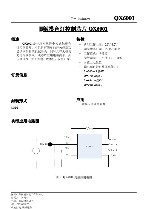
图 4. QX6001 和 QX7135 主灯扩展线性恒流无级调光驱动 LED 应用电路
R C OSC VDD TOU C H CS
DC
Q X 6001
OUT2 OUT1 GND CS GND VDD Q X 7136 DRV
C ref NC
图 5. QX6001 和 QX7136 主灯扩展线性恒流大电流输出无级调光驱动 LED 应用电路
Preliminary
QX6001
触摸台灯控制芯片 QX6001
XL6001原厂规格书(2014版)
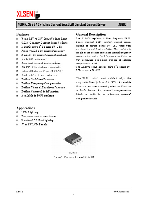
400KHz 32V 2A Switching Current Boost LED Constant Current Driver XL6001Featuresn Wide 3.6V to 24V Input Voltage Rang n0.22V Constant Current Sense Voltage n Directly drive 3~8 Series 1W LEDn Fixed 400KHz Switching Frequency n Max. 2A Switching Current Capability n Up to 92% efficiencyn Excellent line and load regulationn EN PIN TTL shutdown capabilityn Internal Optimize Power MOSFETn Built in LED Open Protectionn Built in Soft-Start Functionn Built in Frequency Compensationn Built in Thermal Shutdown Function n Built in Current Limit Functionn Available in SOP8 package Applicationsn LED Lightingn Boost constant current drivern Monitor LED Backlightingn7’ to 15’ LCD Panels General DescriptionThe XL6001 regulator is fixed frequency PWM Boost (step-up) LED constant current driver, capable of driving Series 1W LED units with excellent line and load regulation. The regulator is simple to use because it includes internal frequency compensation and a fixed-frequency oscillator so that it requires a minimum number of external components to work.The XL6001 could directly drive 5~8 Series 1W LED units at VIN>12V .The PWM control circuit is able to adjust the duty ratio linearly from 0 to 90%. An enable function, an over current protection function is built inside. An internal compensation block is built in to minimize external component count.Figure1. Package Type of XL6001400KHz 32V 2A Switching Current Boost LED Constant Current DriverXL6001Pin ConfigurationsSWEN FB VIN NCSW GNDGNDFigure2. Pin Configuration of XL6001 (Top View)Table 1 Pin DescriptionPin NumberPin Name Description1 ENEnable Pin. Drive EN pin low to turn off the device, drive ithigh to turn it on. Floating is default high.2 VINSupply V oltage Input Pin. XL6001 operates from a 3.6V to 24V DC voltage. Bypass Vin to GND with a suitably large capacitor to eliminate noise on the input.3 FB Feedback Pin (FB). The feedback threshold voltage is 0.22V .4 NC No Connected.5,6 SWPower Switch Output Pin (SW). Output is the switch node thatsupplies power to the output.7,8 GND Ground Pin.400KHz 32V 2A Switching Current Boost LED Constant Current Driver XL6001 Function BlockFigure3. Function Block Diagram of XL6001Typical Application CircuitFigure4. XL6001 Typical Application Circuit400KHz 32V 2A Switching Current Boost LED Constant Current Driver XL6001Ordering InformationPart Number Marking ID Lead Free Lead Free Packing Type XL6001E1 XL6001E1 Tube PackageTemperature RangeXL6001TRE1XL6001E1Tape & ReelXLSEMI Pb-free products, as designated with “E1” suffix in the par number, are RoHS compliant.Absolute Maximum Ratings (Note1)ParameterSymbol Value Unit Input VoltageVin -0.3 to 26 V Feedback Pin Voltage V FB -0.3 to Vin V EN Pin VoltageV EN -0.3 to Vin V Output Switch Pin Voltage V Output -0.3 to 32 V Power DissipationP D Internally limitedmW Thermal Resistance (SOP8)(Junction to Ambient, No Heatsink, Free Air) R JA 100 ºC/W Operating Junction Temperature T J -40 to 125 ºC Storage TemperatureT STG -65 to 150 ºC Lead Temperature (Soldering, 10 sec) T LEAD 260 ºC ESD (HBM)>2000VNote1: Stresses greater than those listed under Maximum Ratings may cause permanent damage to the device. This is a stress rating only and functional operation of the device at these or any other conditions above those indicated in the operation is not implied. Exposure to absolute maximum rating conditions for extended periods may affect reliability.400KHz 32V 2A Switching Current Boost LED Constant Current Driver XL6001 XL6001 Electrical CharacteristicsT a = 25℃;unless otherwise specified.Symbol Parameter Test Condition Min. Typ. Max. Unit System parameters test circuit figure4VFB FeedbackV oltageVin = 5V to 12V, V out=24VIload=100mA209 220 231 mVEfficiency ŋVin=12V ,V out= 6*1W LEDIout=0.3A- 92 - %Electrical Characteristics (DC Parameters)Vin = 12V, GND=0V, Vin & GND parallel connect a 47uf/25V capacitor; Iout=50mA, T a = 25℃; the others floating unless otherwise specified.Parameters Symbol Test Condition Min. Typ. Max. Unit Input operation voltage Vin 3.6 24 V Shutdown Supply Current I STBY V EN=0V 70 100 uAQuiescent Supply Current I q V EN =2V,V FB =Vin2.5 5 mAOscillator Frequency Fosc 320 400 480 Khz Switch Current Limit I L V FB =0 2 AOutput Power NMOS Rdson Vin=12V,I SW=2A110 120 mohmEN Pin Threshold V EN High (Regulator ON)Low (Regulator OFF)1.40.8VI H V EN =2V (ON) 3 10 uA EN Pin Input LeakageCurrent ILV EN =0V (OFF) 3 10 uA Max. Duty Cycle D MAX V FB=0V 90 %400KHz 32V 2A Switching Current Boost LED Constant Current Driver XL6001Schottky Diode Selection TableCurrent SurfaceMountThrough Hole VR (The same as system maximum input voltage)20V 30V 40V 50V60V1A √1N5817 1N5818 1N5819√ 1N5820 1N5821 1N5822√ MBR320 MBR330 MBR340 MBR350 MBR360 √ SK32 SK33 SK34SK35SK36 √ 30WQ03 30WQ04 30WQ05 √ 31DQ03 31DQ04 31DQ05 3A√SR302SR303SR304SR305SR306Typical System Application for VIN=5V to driver 2~6 x 1W series LED unitsFigure5. XL6001 System Parameters Test Circuit (2~6 x 1W LED)400KHz 32V 2A Switching Current Boost LED Constant Current Driver XL6001 Typical System Application for VIN=12V to driver 4~8 x 1W series LED unitsFigure6. XL6001 System Parameters Test Circuit (4~8 x 1W LED)Typical System Application for VIN=12V to driver 4~8 x 1W series LED units With PWM DimmingFigure7. XL6001 System Parameters Test Circuit (4~8 x 1W LED with PWM Dimming)400KHz 32V 2A Switching Current Boost LED Constant Current Driver XL6001 Typical System Application for SEPIC Buck-Boost LED DriverFigure8. XL6001 System Parameters Test Circuit (Buck-Boost LED Driver)400KHz 32V 2A Switching Current Boost LED Constant Current Driver XL6001 Package InformationSOP8 Package Mechanical Dimensions。
bw6101中文规格书
bw6101中文规格书全文共四篇示例,供您参考第一篇示例:BW6101是一款广泛应用于工业领域的高性能传感器,具有稳定的性能和广泛的适用范围。
该传感器在市场上享有很高的声誉,受到了广大用户的信赖和好评。
以下是对BW6101传感器的详细规格介绍。
一、外观和材质BW6101传感器外观精致,采用高强度金属材质制造,表面经过特殊处理,具有防水、防尘、耐腐蚀的特性。
外壳颜色为黑色,外观设计简洁大方,符合工业产品的实用风格。
二、工作原理BW6101传感器采用先进的电子技术,通过内部的传感器元件对周围环境进行实时监测和分析,能够准确地检测目标物体的位置、速度、温度、压力等参数,并将数据传输至控制系统进行处理。
三、性能参数1. 测量范围:根据不同的应用场景和需求,BW6101传感器的测量范围可在一定范围内进行调整,满足不同工况下的需求。
2. 精度:BW6101传感器具有高精度的测量性能,能够实现对目标物体的精准测量,误差范围小,保证了测量数据的准确性。
3. 响应时间:BW6101传感器响应速度快,能够在极短的时间内对目标物体进行识别和测量,适用于对速度和频率要求较高的应用场景。
4. 工作温度:BW6101传感器适用于较宽的工作温度范围,能够在恶劣环境下稳定工作,确保了传感器的稳定性和可靠性。
四、功能特点1. 多种接口:BW6101传感器具有多种接口选择,能够与不同类型的控制系统进行兼容,提高了其应用的灵活性和通用性。
2. 高抗干扰性:BW6101传感器内部集成了高性能的抗干扰技术,能够在复杂的电磁环境下保持稳定的工作表现,减小了外界干扰对传感器的影响。
3. 长寿命:BW6101传感器采用高品质的材料和先进的制造工艺,具有较长的使用寿命,降低了维护成本和更换频率,提高了设备的可靠性。
五、应用领域BW6101传感器广泛应用于工业自动化控制、智能制造、机器人技术、仓储物流等领域,为这些领域的设备和系统提供了稳定可靠的测量数据,发挥了重要作用。
Molex电子技术(LLC) 76155型号产品说明书

GENERAL TOLERANCES(UNLESS SPECIFIED)ANGULAR TOL ±0.5°4 PLACES ±3 PLACES ±2 PLACES ±0.131 PLACE ±0.25THIS DRAWING CONTAINS INFORMATION THAT IS PROPRIETARY TO MOLEX ELECTRONIC TECHNOLOGIES, LLC AND SHOULD NOT BE USED WITHOUT WRITTEN PERMISSIONDIMENSION UNITS SCALE mm 5:1DRWN BY DATETIBARRA2012/11/26CHK'D BYDATEJBINGHAM2012/12/18APPR BYDATEIMPACT 4 PAIR HEADERRIGHT GUIDED ASSEMBLY SALES DRAWINGPRODUCT CUSTOMER DRAWINGM I G R A T E D T O N X2017/09/252017/10/162017/10/183322U N I V E N K A T A A M A S W A M Y A M A S W A M YQUALITY SYMBOLS=0=0=0=0=011X1.3514.8520.8+0.2-0.5�2.95�AB1.90KEY SHOWN IN POSTION "A"TAIL LENGTH1.411.95ZZSECTION Z -Z2.64MINIMUM BOARD1.0014.5P ±0.20(PIN LENGTH)24.6NOTES:1. MATERIALS: HOUSING - LIQUID CRYSTAL POLYMER (LCP) GLASS-FILLED, UL94V-0TERMINALS - HIGH PERFORMANCE COPPER ALLOY 2. FINISH: 30µ MIN GOLD IN CONTACT AREA. SELECTIVE TIN ON PCB TAILS. NICKEL OVERALL.3. REFER TO MOLEX PRODUCT SPECIFICATION PS-76060-999FOR PERFORMANCE SPECIFICATIONS AND ADDITIONAL PCB INFORMATION. 4. THIS PART CONFORMS TO CLASS B REQUIREMENTS OF MOLEX COSMETIC SPEC PS-45499-002. 5. PACKAGE PER: PK-70873-757.6. SEE SHEETS 2 & 3 FOR PART NUMBERS AND BOARD RELATIONSHIPS.7. FOR GROUNDED GUIDE PINS USE DIA. 3.56 +/-0.08 (PTH) DIA. 3.66 (DRILL) AND DIA 6.5 (PAD).8. MATES WITH IMPACT DC SERIES NO. 76160.9. KEEP OUT ZONE FOR BP HOUSING LENGTH INCLUDES AN ADDITIONAL 1.0MM TO ACCOMMODATE FOR SPACE REQUIRED BY DC FRONT HOUSING.10. REFER TO MOLEX PCB ROUTING GUIDE AS-76060-990 FOR ANTIPAD AND ROUTING RECOMMENDATIONS. 11. CONNECTORS SUPPLIED WITH A 2-56 UNC-2A SCREW.12. "THESE DIMENSIONS REPRESENT THE AREA NEEDED TO ACCOMMODATE CONNECTOR INSERTION AND NOTCH DESIGNATESROW AROW A ROW MROW E ROW L ROW D ROW C ROW K ROW J ROW B ROW H ROW F ROW G 3.56⌖⌀0.15UNPLATED SCREW HOLE±0.08⌀SEE NOTE #7SEE PART NUMBER CHART⌖⌀0.10ANDPART NUMBER LOGIC (12 HOLES PER COLUMN)RIGHT GUIDEDBACKPLANE HOLE PATTERN(CONNECTOR SIDE)SEE NOTE 12KEEP-OUT ZONE20.814.8511.422.951.3511XSIGNAL HOLESREFGROUND HOLEREF1.35(ADD FOR END WALL)B 8.504.751.900.95PIN A1BBCCDDEEFFGGHHJJKKLLGENERAL TOLERANCES(UNLESS SPECIFIED)ANGULAR TOL ±0.5°4 PLACES ±3 PLACES ±2 PLACES ±0.131 PLACE ±0.25THIS DRAWING CONTAINS INFORMATION THAT IS PROPRIETARY TO MOLEX ELECTRONIC TECHNOLOGIES, LLC AND SHOULD NOT BE USED WITHOUT WRITTEN PERMISSIONDIMENSION UNITS SCALE mm 4:1DRWN BY DATETIBARRA2012/11/26CHK'D BYDATEJBINGHAM2012/12/18APPR BYDATEIMPACT 4 PAIR HEADERRIGHT GUIDED ASSEMBLY SALES DRAWINGPRODUCT CUSTOMER DRAWINGM I G R A T E D T O N X2017/09/252017/10/162017/10/183322U N I V E N K A T A A M A S W A M Y A M A S W A M YQUALITY SYMBOLS=0=0=0=0=0MATERIAL NUMBER # OF COLUMNS # OF DIFF PAIR DIM "A"DIM "B"GUIDE RIGHT OPEN WALL OPTION76155-*3**62417.99.5076155-*8**83221.713.3076155-*1**104025.517.1076155-*6**166436.928.50MATERIAL NUMBER # OF COLUMNS # OF DIFF PAIR DIM "A"DIM "B"GUIDE RIGHT END WALL OPTION76155-*3**62419.39.5076155-*8**83223.113.3076155-*1**104026.917.1076155-*6**166438.328.50PART NUMBER TABLEPART NUMBER LOGICGUIDE RIGHT END WALL OPTIONGUIDE RIGHT OPEN WALL OPTION76155-****MODULE TYPE5 = GUIDE RIGHT, TIN9 = GUIDE RIGHT END WALL, TINMODULE TYPE 1 = 10 COL 3 = 6 COL 6 = 16 COL 8 = 8 COLKEY ORIENTATION 0 = NO KEY 1 = A 2 = B 3 = C 4 = D 5 = E 6 = F 7 = G 8 = HPIN LENGTH (P)3 = 4.50 (SHORT COMPLIANT, 0.46±0.05 PTH)4 = 4.90 (SHORT COMPLIANT, 0.46±0.05 PTH)5 = 5.50 (SHORT COMPLIANT, 0.46±0.05 PTH)6 = 4.50 (MICRO COMPLIANT, 0.39±0.05 PTH)7 = 4.90 (MICRO COMPLIANT, 0.39±0.05 PTH)8 = 5.50 (MICRO COMPLIANT, 0.39±0.05 PTH)BBCCDDE EF FGGH HJ JKKGENERAL TOLERANCES(UNLESS SPECIFIED)ANGULAR TOL ±0.5°4 PLACES ±3 PLACES ±2 PLACES ±0.131 PLACE ±0.25THIS DRAWING CONTAINS INFORMATION THAT IS PROPRIETARY TO MOLEX ELECTRONIC TECHNOLOGIES, LLC AND SHOULD NOT BE USED WITHOUT WRITTEN PERMISSIONDIMENSION UNITS SCALE mm 1:1DRWN BY DATETIBARRA2012/11/26CHK'D BYDATEJBINGHAM2012/12/18APPR BYDATEIMPACT 4 PAIR HEADERRIGHT GUIDED ASSEMBLY SALES DRAWINGPRODUCT CUSTOMER DRAWINGM I G R A T E D T O N X2017/09/252017/10/162017/10/183322U N I V E N K A T A A M A S W A M Y A M A S W A M YQUALITY SYMBOLS=0=0=0=0=00.35OFFSET BETWEEN DC ANDBP HOLE COLUMNSDCARD ROW ABP HOLE COLUMN (COLUMN 10 REF)BPLANE PCBDCARD PCBDC HOLE COLUMN (COLUMN 10 REF)BPLANE PCBDCARD PCBBP ROW A14.0DCARD ROW AB P R O W A11.953.020.8IMPACT 4 PAIRBOARD RELATIONSHIPSBBCCDDEEFFG GHHJ JKK。
Ra-01S规格书说明书
Ra-01S规格书版本V1.1版权©2020免责申明和版权公告本文中的信息,包括供参考的URL地址,如有变更,恕不另行通知。
文档“按现状”提供,不负任何担保责任,包括对适销性、适用于特定用途或非侵权性的任何担保,和任何提案、规格或样品在他处提到的任何担保。
本文档不负任何责任,包括使用本文档内信息产生的侵犯任何专利权行为的责任。
本文档在此未以禁止反言或其他方式授予任何知识产权使用许可,不管是明示许可还是暗示许可。
文中所得测试数据均为安信可实验室测试所得,实际结果可能略有差异。
文中提到的所有商标名称、商标和注册商标均属其各自所有者的财产,特此声明。
最终解释权归深圳市安信可科技有限公司所有。
注意由于产品版本升级或其他原因,本手册内容有可能变更。
深圳市安信可科技有限公司保留在没有任何通知或者提示的情况下对本手册的内容进行修改的权利。
本手册仅作为使用指导,深圳市安信可科技有限公司尽全力在本手册中提供准确的信息,但是深圳市安信可科技有限公司并不确保手册内容完全没有错误,本手册中的所有陈述、信息和建议也不构成任何明示或暗示的担保。
文件制定/修订/废止履历表版本日期制定/修订内容制定核准V1.02020.8.12首版徐V1.12020.8.19更新部分参数徐目录一、产品概述 (5)二、电气参数 (6)三、外观尺寸 (8)四、管脚定义 (10)五、原理图 (11)六、设计指导 (12)七、回流焊曲线图 (14)八、包装信息 (15)九、联系我们 (15)一、产品概述安信可LoRa系列模块(Ra-01S)由安信可科技设计开发。
该模组用于超长距离扩频通信,其射频芯片SX1268主要采用LoRa™远程调制解调器,用于超长距离扩频通信,抗干扰性强,能够最大限度降低电流消耗。
借助SEMTECH的LoRa™专利调制技术,SX1268具有超过-148dBm的高灵敏度,+22dBm的功率输出,传输距离远,可靠性高。
同时,相对传统调制技术,LoRa™调制技术在抗阻塞和选择方面也具有明显优势,解决了传统设计方案无法同时兼顾距离、抗干扰和功耗的问题。
NZB6001 微机 PT 测控装置 使用说明书
目录
1 概述................................................................................................................................................. 1 1.1 适用范围.....................................................................................................................................1 1.2 功能配置.....................................................................................................................................1 1.3 性能特点.....................................................................................................................................1 2 技术性能及电气参数.....................................................................................................................2 2.1 额定电气参数...............................................................................
XL4001 DEMO board 说明书
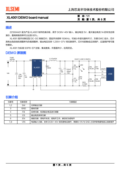
页数:第1 页,共5 页描述221004A01是为产品XL4001制作的演示板,用于DC8V~40V输入,输出电压5V,最大输出电流1A的车充应用演示,最高转换效率可以达到83%。
XL4001是开关降压型DC-DC转换芯片;固定开关频率150KHz,可减小外部元器件尺寸,方便EMC设计。
芯片具有出色的线性调整率与负载调整率,输出电压支持1.235V~37V间任意调节。
芯片内部集成过流保护、过温保护等可靠性模块。
XL4001为标准SOP8-EP封装,集成度高,外围器件少,应用灵活。
DEMO原理图FUSE引脚介绍页数:第2 页,共5 页物料清单页数:第3 页,共5 页性能数据转换效率转换效率:线性调整率和负载调整率:Efficiency VS Load currentEfficiency(%)Load current(A)Output voltage VS Output currentOutputvoltage(V)Output current(A)页 数:第 4 页, 共 5 页DEMO 实物图PCB 布局顶层底层页数:第5 页,共5 页应用信息输入电容选择在连续模式中,转换器的输入电流是一组占空比约为VOUT/VIN的方波。
为了防止大的瞬态电压,必须采用针对最大RMS电流要求而选择低ESR(等效串联电阻)输入电容器。
对于大多数的应用,1个4.7uF的输入电容器就足够了,它的放置位置尽可能靠近XL4001的位置上。
最大RMS电容器电流由下式给出:IRMS≈IMAX*√VOUT(VIN-VOUT)VIN其中,最大平均输出电流IMAX等于峰值电流与1/2峰值纹波电流之差,即IMAX=ILIM-△IL/2。
在未使用陶瓷电容器时,还建议在输入电容上增加一个0.1uF至1uF的陶瓷电容器以进行高频去耦。
输出电容选择在输出端应选择低ESR电容以减小输出纹波电压,一般来说,一旦电容ESR得到满足,电容就足以满足需求。
- 1、下载文档前请自行甄别文档内容的完整性,平台不提供额外的编辑、内容补充、找答案等附加服务。
- 2、"仅部分预览"的文档,不可在线预览部分如存在完整性等问题,可反馈申请退款(可完整预览的文档不适用该条件!)。
- 3、如文档侵犯您的权益,请联系客服反馈,我们会尽快为您处理(人工客服工作时间:9:00-18:30)。
400KHz 32V 2A Switching Current Boost LED Constant Current Driver XL6001Featuresn Wide 3.6V to 24V Input Voltage Rang n 0.22V Constant Current Sense Voltage n Directly drive 3~8 Series 1W LED n Fixed 400KHz Switching Frequency n Max. 2A Switching Current Capability n Up to 92% efficiencyn Excellent line and load regulation n EN PIN TTL shutdown capability n Internal Optimize Power MOSFET n Built in LED Open Protection n Built in Soft-Start Functionn Built in Frequency Compensation n Built in Thermal Shutdown Function nBuilt in Current Limit Function n Available in SOP8 package Applicationsn LED Lightingn Boost constant current driver n Monitor LED Backlighting n 7’ to 15’ LCD PanelsGeneral DescriptionThe XL6001 regulator is fixed frequency PWM Boost (step-up) LED constant current driver, capable of driving Series 1W LED units with excellent line and load regulation. The regulator is simple to use because it includes internal frequency compensation and a fixed-frequency oscillator so that it requires a minimum number of external components to work.The XL6001 could directly drive 5~8 Series 1W LED units at VIN>12V .The PWM control circuit is able to adjust the duty ratio linearly from 0 to 90%. An enable function, an over current protection function is built inside. An internal compensation block is built in to minimize external component count.Figure1. Package Type of XL6001400KHz 32V 2A Switching Current Boost LED Constant Current DriverXL6001Pin ConfigurationsSWEN FB VIN NCSW GNDGNDFigure2. Pin Configuration of XL6001 (Top View)Table 1 Pin DescriptionPin NumberPin Name Description1 ENEnable Pin. Drive EN pin low to turn off the device, drive ithigh to turn it on. Floating is default high.2 VINSupply V oltage Input Pin. XL6001 operates from a 3.6V to 24V DC voltage. Bypass Vin to GND with a suitably large capacitor to eliminate noise on the input.3 FB Feedback Pin (FB). The feedback threshold voltage is 0.22V .4 NC No Connected.5,6 SWPower Switch Output Pin (SW). Output is the switch node thatsupplies power to the output.7,8 GND Ground Pin.400KHz 32V 2A Switching Current Boost LED Constant Current Driver XL6001 Function BlockFigure3. Function Block Diagram of XL6001Typical Application CircuitFigure4. XL6001 Typical Application Circuit400KHz 32V 2A Switching Current Boost LED Constant Current Driver XL6001Ordering InformationPart Number Marking ID Lead Free Lead Free Packing Type XL6001E1 XL6001E1 Tube PackageTemperature RangeXL6001TRE1XL6001E1Tape & ReelXLSEMI Pb-free products, as designated with “E1” suffix in the par number, are RoHS compliant.Absolute Maximum Ratings (Note1)ParameterSymbol Value Unit Input VoltageVin -0.3 to 26 V Feedback Pin Voltage V FB -0.3 to Vin V EN Pin VoltageV EN -0.3 to Vin V Output Switch Pin Voltage V Output -0.3 to 32 V Power DissipationP D Internally limitedmW Thermal Resistance (SOP8)(Junction to Ambient, No Heatsink, Free Air) R JA 100 ºC/W Operating Junction Temperature T J -40 to 125 ºC Storage TemperatureT STG -65 to 150 ºC Lead Temperature (Soldering, 10 sec) T LEAD 260 ºC ESD (HBM)>2000VNote1: Stresses greater than those listed under Maximum Ratings may cause permanent damage to the device. This is a stress rating only and functional operation of the device at these or any other conditions above those indicated in the operation is not implied. Exposure to absolute maximum rating conditions for extended periods may affect reliability.400KHz 32V 2A Switching Current Boost LED Constant Current Driver XL6001 XL6001 Electrical CharacteristicsT a = 25℃;unless otherwise specified.Symbol Parameter Test Condition Min. Typ. Max. Unit System parameters test circuit figure4VFB FeedbackV oltageVin = 5V to 12V, V out=24VIload=100mA209 220 231 mVEfficiency ŋVin=12V ,V out= 6*1W LEDIout=0.3A- 92 - %Electrical Characteristics (DC Parameters)Vin = 12V, GND=0V, Vin & GND parallel connect a 47uf/25V capacitor; Iout=50mA, T a = 25℃; the others floating unless otherwise specified.Parameters Symbol Test Condition Min. Typ. Max. Unit Input operation voltage Vin 3.6 24 V Shutdown Supply Current I STBY V EN=0V 70 100 uAQuiescent Supply Current I q V EN =2V,V FB =Vin2.5 5 mAOscillator Frequency Fosc 320 400 480 Khz Switch Current Limit I L V FB =0 2 AOutput Power NMOS Rdson Vin=12V,I SW=2A110 120 mohmEN Pin Threshold V EN High (Regulator ON)Low (Regulator OFF)1.40.8VI H V EN =2V (ON) 3 10 uA EN Pin Input LeakageCurrent ILV EN =0V (OFF) 3 10 uA Max. Duty Cycle D MAX V FB=0V 90 %400KHz 32V 2A Switching Current Boost LED Constant Current Driver XL6001Schottky Diode Selection TableCurrent SurfaceMountThrough Hole VR (The same as system maximum input voltage)20V 30V 40V 50V60V1A √1N5817 1N5818 1N5819√ 1N5820 1N5821 1N5822√ MBR320 MBR330 MBR340 MBR350 MBR360 √ SK32 SK33 SK34SK35SK36 √ 30WQ03 30WQ04 30WQ05 √ 31DQ03 31DQ04 31DQ05 3A√SR302SR303SR304SR305SR306Typical System Application for VIN=5V to driver 2~6 x 1W series LED unitsFigure5. XL6001 System Parameters Test Circuit (2~6 x 1W LED)400KHz 32V 2A Switching Current Boost LED Constant Current Driver XL6001 Typical System Application for VIN=12V to driver 4~8 x 1W series LED unitsFigure6. XL6001 System Parameters Test Circuit (4~8 x 1W LED)Typical System Application for VIN=12V to driver 4~8 x 1W series LED units With PWM DimmingFigure7. XL6001 System Parameters Test Circuit (4~8 x 1W LED with PWM Dimming)400KHz 32V 2A Switching Current Boost LED Constant Current Driver XL6001 Typical System Application for SEPIC Buck-Boost LED DriverFigure8. XL6001 System Parameters Test Circuit (Buck-Boost LED Driver)400KHz 32V 2A Switching Current Boost LED Constant Current Driver XL6001 Package InformationSOP8 Package Mechanical Dimensions。