MA4SPS402中文资料
GWF402中文资料

GAMEWELL-FCI12 Clintonville Road, Northford, CT 06472-1610 USA • Tel: (203) 484-7161 • Fax: (203) 484-7118Specifications are for information only, are not intended for installation purposes, and are subject to change without notice. No responsibility is assumed by Gamewell-FCI for their use.©2007 by Honeywell International Inc. All rights 9021-60292 Rev. A page 1 of 2Flex Series GWF402 andGWF4042 and 4 Zone ConventionalFire Alarm Control PanelsSIGNALINGS521MEAApprove d366-04-E 7165-1288:180An ISO 9000-2000 CompanyDescriptioni 3™ is a trademark of Honeywell International Inc.UL ® is a registered trademark of Underwriter’s Laboratories Inc.The Flex 402 is a two zone fire alarm control panel (FACP)and the Flex 404 is a four zone FACP . These control pan-els provide reliable fire signaling protection for small to medium sized retail, office, multi-family, or other similar commercial or institutional building. Initiating device circuits (IDCs) for Flex Series panels are power limited and operate in Style B (Class B). Each panel is compatible with conventional input devices such as two-wire smoke detectors, four-wire smoke detectors, pull sta-tions, water flow devices, tamper switches and other nor-mally-open contact devices. This includes System Sensori 3™ Series microprocessor-based detectors with advancedfeatures like drift compensation, maintenance alert and freeze warning. (See Device Compatibility Document PN 52195 for a listing of compatible devices.)Outputs include one notification appliance circuit (NAC) on the Flex 402 and two NACs on the Flex 404. NACs are power limited and operate in Style Y (Class B). Each FACP has a Form-C Alarm and Trouble relay and 24 VDC special applications resettable power. In addition, the Flex 404 has a Form-C Supervisory relay and a special application non-resettable power output. The FACP supervises wiring, AC voltage and battery level.Activation of a compatible smoke detector or any normally-open fire alarm initiating device will activate audible and visual signaling devices, illuminate an indicating LED,sound the piezo sounder at the FACP , activate the FACP alarm relay and operate and optional modules used to notify a remote station or initiate an auxiliary control function.Both the Flex 402 and Flex 404 fire alarm control panels are listed to UL ® Standard 864, 9th Edition.Features•Flex 402: Two Style B (Class B) IDC zones, one Style Y (Class B) NAC•Flex 404: Four Style B (Class B) IDC zones, two Style Y (Class B) NACs•Optional NAC Class A converter module (Flex 404)•NAC synchronization and programmability features:- ADA compliant strobe synchronization- ANSI audible signals as required by NFPA 72- Silence inhibit, auto-silence, non-silenceable - Selective Silence: mute horns, keep strobes lit - Temporal or steady signal•Silent or audible walk test from front keypad•Zone disable, alarm verification selectable per zone •Controls: Acknowledge, Alarm, Silence, Reset, Walktest, Zone enable/disable•LED indicators: Alarm, Supervisory, Maintenance, Trouble (one per zone): AC, NAC / Zone disable, NAC fault, System / Power Trouble, Walktest, Alarm Silence, Charger / Battery / Earth Fault (on pcb) •Alarm verification•Low AC voltage sense, automatic battery charger •Piezo sounder for alarm, trouble, and supervisoryGWF402 (left) and GWF404 (right)GAMEWELL-FCI12 Clintonville Road, Northford, CT 06472-1610 USA • Tel: (203) 484-7161 • Fax: (203) 484-71189021-60292 Rev. A page 2 of 2 OptionsCAC-4Used to convert Style B (Class B) IDCs toStyle D (Class A) and Style Y (Class B) NACs to Style Z (Class A). Mounts inFACP . Flex 404 only.XRM-24Second 100VA transformer for maximumaccessory power. Mounts in FACP . Flex 404 only.4XTMF Transmitter module provides output forlocal energy municipal box transmitter and alarm and trouble reverse polarity. Mounts in FACP . Flex 402 & Flex 404.4XZMF Zone relay module provides Form-C relays:Alarm Zones 1, 2, 3, 4, System Alarm, Trouble. Mounts in FACP . Flex 404 only.4XLMF LED interface module supports theGWSAN-404 remote annunciator,supervises annunciator wiring for open conditions. Mounts in FACP . Flex 404 only.411UD Four input/channel, dual line, digital alarmcommunicator/transmitter(DACT). Input/channels are compatible with normally open relay contacts, are supervised and fully programmable. Interfaces with public switched telephone networks andcompatible with most central station receiv-ers. Flex 404 only.GWSAN-404Remote annunciator mounts in single-gangelectrical box, provides LED indication of Alarm Zones 1, 2, 3, 4; and System Trouble. Flex 404 only.SpecificationsAC Power 120 VAC, 50/60Hz, 2.3 ABatteryMax. charging circuit: 27.6 VDC@ 0.8A Max. charger capacity: 18 Ah (two 7Ah batteries fit inside FACP)Initiating Device Alarm zones 1 & 2 (Flex 402 / Flex 404)Circuits (IDC)Alarm zones 3 & 4 (Flex 404 only)Operation: All zones Style B (Class B)Power limited circuitryOperating voltage: nominal 20 VDC Alarm current: 15 mA minimumShort circuit current: 40 mA maximum Standby current: 4 mAMaximum loop resistance: 100 ohms NotificationOne NAC: Flex 402; two NACs:Flex 404Specifications (Continued)Circuits (NAC)Operation: Style Y (Class B)Power limited circuitryOperating voltage: nominal 24 VDC Maximum signaling current: 2.5 A total (5.0 A Flex 404 with optional transformer)Maximum line impedance: 1.5 volt dropForm-C Relays Trouble, Alarm (Supervisory, Flex 404)Contact ratings 2 A @ 30 VAC (resistive)Resettable Operating voltage: nominal 24 VDC powerPower limited circuitryMaximum available current: 500 mANonresettable Operating voltage: nominal 24 VDC power Power limited circuitryMaximum Available current: 500 mA CabinetDoor: 15.3" x 14.7" x 0.3" (39 x 37 x 1 cm)Backbox: 15.0" x 14.5" x 3.0"(38 x 37 x 8 cm)Ordering InformationGWF402Flex 402 conventional FACP , 2 zones, 120 VAC, redGWF404Flex 404 conventional FACP , 4 zones, 120 VAC, red71252EOL resistor, 4.7K ohm, ½ watt52194Flex 402 and Flex 404 Installation & Operation ManualOptions:CAC-4Class A converter for initiating device circuits and notification appliance cir-cuits (cannot be used on Flex 402)XRM-24Transformer, expands NAC circuit power from 3 to 5 amps4XTMF Transmitter module for remote station output or municipal box connection 4XZMF Relay module, four relays-by-zone, alarm and trouble contacts, 24VDC 4XLMF Remote annunciator driver, 24 VDC, supports GWSAN-404411UDFour channel dual slave programmer DACT, Form C relay and upload/down-load capability; with enclosure, requires PRO-411PRO-411Programmer, use with 411UD, 411UDACGWSAN-404LED remote annunciator for Flex 404, 4 alarms, 1 trouble (requires 4XLMF)BB-17FBattery box, houses 2 batteries (7-18 Ah max)。
M54HC4020_04资料

1/11May 2004sHIGH SPEED:f MAX =70MHz (TYP .)at V CC =6V sLOW POWER DISSIPATION:I CC =4µA(MAX.)at T A =25°C sHIGH NOISE IMMUNITY:V NIH =V NIL =28%V CC (MIN.)sSYMMETRICAL OUTPUT IMPEDANCE:|I OH |=I OL =4mA (MIN)sBALANCED PROPAGATION DELAYS:t PLH ≅t PHLsWIDE OPERATING VOLTAGE RANGE:V CC (OPR)=2V to 6VsPIN AND FUNCTION COMPATIBLE WITH 54SERIES 4020s SPACE GRADE-1:ESA SCC QUALIFIED s50krad QUALIFIED,100krad AVAILABLE ON REQUESTsNO SEL UNDER HIGH LET HEAVY IONS IRRADIATIONsDEVICE FULLY COMPLIANT WITH SCC-9204-070DESCRIPTIONThe M54HC4020is an high speed CMOS 14STAGE BINARY COUNTER fabricated with silicon gate C 2MOS technology.A clear input is used to reset the counter to the all low level state.A high level on CLEAR accomplishes the reset function.A negative transition on the CLOCK input increments the counter by one.For M54HC4020twelve kind of divided output are provided;1st and 4th stage to 14th stage.The maximum division available at last stage is 1/16384x f IN at clock.All inputs are equipped with protection circuits against static discharge and transient excess voltage.M54HC4020RAD-HARD 14STAGE BINARYCOUNTERPIN CONNECTIONORDER CODESPACKAGE FM EM DILC M54HC4020D M54HC4020D1FPCM54HC4020KM54HC4020K1M54HC40202/11Figure 1:IEC Logic SymbolsFigure 2:Input And Output Equivalent Circuit Table 1:Pin DescriptionTable 2:TruthTablePIN N°SYMBOL NAME AND FUNCTION 9,7,6,5,3,2,4,13,12,14,15,1Q1,Q4to Q14Parallel Outputs 10CLOCK Clock Input (LOW toHIGH,Edge Triggered)11CLEAR Reset Inputs 8GND Ground (0V)16V CCPositive Supply VoltageM54HC40203/11Figure 3:Logic DiagramThis logic diagram has not be used to estimate propagation delaysTable 3:Absolute Maximum RatingsAbsolute Maximum Ratings are those values beyond which damage to the device may occur.Functional operation under these conditions is not impliedSymbol ParameterValue Unit V CC Supply Voltage -0.5to +7V V I DC Input Voltage -0.5to V CC +0.5V V O DC Output Voltage -0.5to V CC +0.5V I IK DC Input Diode Current ±20mA I OK DC Output Diode Current ±20mA I ODC Output Current±25mA I CC or I GND DC V CC or Ground Current±50mA P D Power Dissipation300mW T stg Storage Temperature -65to +150°C T LLead Temperature (10sec)265°CM54HC40204/11Table 4:Recommended Operating ConditionsTable 5:Dc SpecificationsSymbol ParameterValue Unit V CC Supply Voltage 2to 6V V I Input Voltage 0to V CC V V O Output Voltage 0to V CC V T op Operating Temperature -55to 125°C t r ,t fInput Rise and Fall TimeV CC =2.0V 0to 1000ns V CC =4.5V 0to 500ns V CC =6.0V0to 400nsSymbolParameterTest ConditionValue UnitV CC (V)T A =25°C -40to 85°C -55to 125°C Min.Typ.Max.Min.Max.Min.Max.V IHHigh Level Input Voltage 2.0 1.5 1.5 1.5V 4.5 3.15 3.15 3.156.0 4.24.24.2V ILLow Level Input Voltage2.00.50.50.5V4.5 1.35 1.35 1.356.0 1.81.81.8V OHHigh Level Output Voltage2.0I O =-20µA 1.9 2.0 1.9 1.9V4.5I O =-20µA 4.4 4.5 4.4 4.46.0I O =-20µA5.96.0 5.9 5.94.5I O =-4.0mA 4.18 4.31 4.13 4.106.0I O =-5.2mA 5.685.8 5.635.60V OLLow Level Output Voltage2.0I O =20µA 0.00.10.10.1V 4.5I O =20µA 0.00.10.10.16.0I O =20µA 0.00.10.10.14.5I O =4.0mA 0.170.260.330.406.0I O =5.2mA 0.180.260.330.40I I Input Leakage Current6.0V I =V CC or GND ±0.1±1±1µA I CCQuiescent Supply Current6.0V I =V CC or GND44080µAM54HC40205/11Table 6:AC Electrical Characteristics (C L =50pF,Input t r =t f =6ns)Table 7:Capacitive Characteristics1)C PD is defined as the value of the IC’s internal equivalent capacitance which is calculated from the operating current consumption without load.(Refer to Test Circuit).Average operating current can be obtained by the following equation.I CC(opr)=C PD x V CC x f IN +I CC /2(per FLIP/FLOP)SymbolParameterTest ConditionValue UnitV CC (V)T A =25°C -40to 85°C -55to 125°C Min.Typ.Max.Min.Max.Min.Max.t TLH t THL Output TransitionTime 2.0307595110ns 4.581519226.07131619t PLH t PHL Propagation DelayTime(Qn -Qn+1) 2.020506575ns4.551013156.0491113t PLH t PHL Propagation DelayTime(CLOCK Q1) 2.076145180220ns4.5212936446.018253138t PHLPropagation Delay Time(CLEAR -Qn) 2.060140175210ns4.5182835426.015243036f MAXMaximum Clock Frequency 2.0 6.015 4.84MHz4.5306524206.035702824t W(H)t W(L)Minimum Pulse Width (CLOCK) 2.0407595110ns4.581519226.07131619t W(H)Minimum Pulse Width (CLEAR) 2.0327595110ns4.581519226.07131619t REMMinimum Removal Time2.0000ns4.50006.0SymbolParameterTest ConditionValue UnitV CC (V)T A =25°C -40to 85°C -55to 125°C Min.Typ.Max.Min.Max.Min.Max.C IN Input Capacitance 5.05101010pF C PDPower Dissipation Capacitance (note 1)5.034pFM54HC40206/11Figure 4:Test CircuitC L =50pF or equivalent (includes jig and probe capacitance)R T =Z OUT of pulse generator (typically 50Ω)Figure 5:Waveform -Minimum Pulse Width (Clear)And Removal Time (Clear To Clock)(f=1MHz;50%dutycycle)M54HC4020 Figure6:Waveform-Propagation Delay Time(f=1MHz;50%duty cycle)Figure7:Waveform-Propagation Delay Time,Minimum Pulse Width(Clock)(f=1MHz;50%duty cycle)7/11M54HC40208/11DIM.mm.inchMIN.TYP MAX.MIN.TYP.MAX.A 2.1 2.710.0830.107 a1 3.00 3.700.1180.146 a20.630.88 1.140.0250.0350.045B 1.82 2.390.0720.094 b0.400.450.500.0160.0180.020 b10.200.2540.300.0080.0100.012 D20.0620.3220.580.7900.8000.810 e7.367.627.870.2900.3000.310 e1 2.540.100e217.6517.7817.900.6950.7000.705 e37.627.878.120.3000.3100.320 F7.297.497.700.2870.2950.303 I 3.830.151 K10.9012.10.4290.476 L 1.14 1.50.0450.059DILC-16 MECHANICAL DATA0056437FM54HC40209/11DIM.mm.inchMIN.TYP MAX.MIN.TYP.MAX.A 6.75 6.917.060.2660.2720.278B 9.769.9410.140.3840.3920.399C 1.49 1.950.0590.077D 0.1020.1270.1520.0040.0050.006E 8.768.899.010.3450.3500.355F 1.270.050G 0.380.430.480.0150.0170.019H 6.00.237L 18.7522.00.7380.867M 0.330.380.430.0130.0150.017N4.310.170FPC-16 MECHANICAL DATA0016030E1816FG DHA BMCNH9ELM54HC4020Table8:Revision HistoryDate Revision Description of Changes 10-May-20041First Release10/11M54HC4020 Information furnished is believed to be accurate and reliable. However, STMicroelectronics assumes no responsibility for the consequences of use of such information nor for any infringement of patents or other rights of third parties which may result from its use. No license is granted by implication or otherwise under any patent or patent rights of STMicroelectronics. Specifications mentioned in this publication are subject to change without notice. This publication supersedes and replaces all information previously supplied. STMicroelectronics products are not authorized for use as critical components in life support devices or systems without express written approval of STMicroelectronics.The ST logo is a registered trademark of STMicroelectronicsAll other names are the property of their respective owners© 2004 STMicroelectronics - All Rights ReservedSTMicroelectronics GROUP OF COMPANIESAustralia - Belgium - Brazil - Canada - China - Czech Republic - Finland - France - Germany - Hong Kong - India - Israel - Italy - Japan - Malaysia - Malta - Morocco - Singapore - Spain - Sweden - Switzerland - United Kingdom - United States.11/11。
2SK4042中文资料

TOSHIBA Field Effect Transistor Silicon N Channel MOS Type (π-MOSVI)2SK4042Switching Regulator Applications• Low drain-source ON resistance: R DS (ON) = 0.7Ω (typ.) • High forward transfer admittance: |Y fs | = 6.5S (typ.) • Low leakage current: I DSS = 100 μA (V DS = 500 V)• Enhancement mode: V th = 2.0~4.0 V (V DS = 10 V , I D = 1 mA)Absolute Maximum Ratings (Ta = 25°C)Characteristics Symbol Rating UnitDrain-source voltageV DSS500 V Drain-gate voltage (R GS = 20 k Ω) V DGR500 V Gate-source voltageV GSS ±30 V DC (Note 1)I D8 Drain currentPulse (t = 1 ms)(Note 1) IDP32ADrain power dissipation (Tc = 25°C)P D40 WSingle pulse avalanche energy(Note 2)E AS312 mJ Avalanche currentI AR 8 ARepetitive avalanche energy (Note 3) E AR 4 mJChannel temperature T ch 150 °CStorage temperature rangeT stg-55~150 °CNote: Using continuously under heavy loads (e.g. the application of high temperature/current/voltage and the significant change intemperature, etc.) may cause this product to decrease in the reliability significantly even if the operating conditions (i.e. operating temperature/current/voltage, etc.) are within the absolute maximum ratings. Please design the appropriate reliability upon reviewing the Toshiba Semiconductor Reliability Handbook (“Handling Precautions”/’’Derating Concept and Methods’’) and individual reliability data (i.e. reliability test report and estimated failure rate, etc).Thermal CharacteristicsCharacteristics Symbol Max UnitThermal resistance, channel to case R th (ch-c) 3.125 °C/W Thermal resistance, channel to ambientR th (ch-a) 62.5 °C/WNote 1: Ensure that the channel temperature does not exceed 150°C. Note 2: V DD = 90 V, T ch = 25°C(initial), L = 8.3 mH, I AR = 8 A, R G = 25 Ω Note 3: Repetitive rating: pulse width limited by maximum channel temperature This transistor is an electrostatic-sensitive device. Please handle with caution.Unit: mm1: Gate2: Drain 3: SourceJEDEC ―JEITA SC-67 TOSHIBA 2-10U1BWeight : 1.7 g (typ.)Electrical Characteristics (Ta = 25°C)Source-Drain Ratings and Characteristics (Ta = 25°C)Characteristics Symbol Test Condition Min Typ. Max UnitContinuous drain reverse current(Note 1) I DR ⎯⎯ ⎯ 8 A Pulse drain reverse current (Note 1)I DRP ⎯⎯ ⎯ 32 A Forward voltage (diode) V DSF I DR = 8 A, V GS = 0 V ⎯⎯−1.7VReverse recovery time t rr ⎯ 190 ⎯ ns Reverse recovery chargeQ rrI DR = 8 A, V GS = 0 V, dI DR /dt = 100 A/μs⎯ 0.5 ⎯μCMarkingLead (Pb)-Free FinishK4042816200102030 1245040⎪Y fs ⎪ – I DGATE-SOURCE VOLTAGE V GS (V)I D – V GSGATE-SOURCE VOLTAGE V GS(V) D R A I N C U R R E N TI D (A )D R A I N -S O U R CE V O L T A G E V D S (V )V DS – V GSDRAIN CURRENT I D (A) F O R W A R D T R A N S F E R A D M I T T A N C E⎪Y f s ⎪ (S )DRAIN-SOURCE VOLTAGE V DS(V)I D – V DSD R A I N C U R RE N T I D (A )DRAIN-SOURCE VOLTAGE V DS (V)I D – V DSD R A I N C U R RE N T I D (A )R DS (ON) – I DDRAIN CURRENT I D (A)D R A I N -S O U R CE O N R E S I S T A N C E R D S (O N ) (Ω)2 4 6 8 104 8 2610 00682015 410510 20.10.11101210DRAIN-SOURCE VOLTAGE V DS (V)CAPACITANCE – V DSC A P A C I T A N C E C (p F )0.11 10 100CASE TEMPERATURE Tc (°C)D R A I N -S O U R CE O N R E SI S T A N C E R D S (O N ) ( Ω)D R A I N P O WE RD I S S I P A T I O N P D (W )CASE TEMPERATURE Tc (°C)P D – TcI DR – V DSDRAIN-SOURCE VOLTAGE V DS (V)D R A I N RE V E R S E C U R R E N T I D R (A )TOTAL GATE CHARGE Q g (nC)G A T E -S O U R C E V O L T A G E V G S (V )DYNAMIC INPUT / OUTPUTCHARACTERISTICSD R A I N -S O U R CE V O L T A G E V D S (V )0 10 20 3050404V th – TcG A T E T H R E S H O L D V O L T A G E V t h (V )CASE TEMPERATURE Tc (°C)−80−40 0 4080 120 1602COMMON SOURCE 0 40 80 120 160R – TCHANNEL TEMPERATURE (INITIAL)T ch (°C)E AS – T chA VA L A N C H E EN E R G YE A S (m J )r th – t wPULSE WIDTH t w (s)0.001N O R MA L I Z E D T R A N S I E N T T H E R MA L I M P E D A N C E r t h (t )/R t h (c h -c )−15 15 TEST CIRCUITWAVE FORMBR G = 25 ΩV DD = 90 V, L = 8.3mH⎟⎟⎠⎞⎜⎜⎝⎛−⋅⋅⋅=V DD B VDSS B VDSS 2I L 21ΕAS25 50 75 100 125150DRAIN-SOURCE VOLTAGE V DS (V)SAFE OPERATING AREAD R A I N C U R RE N T I D (A )RESTRICTIONS ON PRODUCT USE20070701-EN GENERAL •The information contained herein is subject to change without notice.•TOSHIBA is continually working to improve the quality and reliability of its products. Nevertheless, semiconductor devices in general can malfunction or fail due to their inherent electrical sensitivity and vulnerability to physical stress. It is the responsibility of the buyer, when utilizing TOSHIBA products, to comply with the standards of safety in making a safe design for the entire system, and to avoid situations in which a malfunction or failure of such TOSHIBA products could cause loss of human life, bodily injury or damage to property.In developing your designs, please ensure that TOSHIBA products are used within specified operating ranges as set forth in the most recent TOSHIBA products specifications. Also, please keep in mind the precautions and conditions set forth in the “Handling Guide for Semiconductor Devices,” or “TOSHIBA Semiconductor Reliability Handbook” etc.• The TOSHIBA products listed in this document are intended for usage in general electronics applications (computer, personal equipment, office equipment, measuring equipment, industrial robotics, domestic appliances, etc.).These TOSHIBA products are neither intended nor warranted for usage in equipment that requires extraordinarily high quality and/or reliability or a malfunction or failure of which may cause loss of human life or bodily injury (“Unintended Usage”). Unintended Usage include atomic energy control instruments, airplane or spaceship instruments, transportation instruments, traffic signal instruments, combustion control instruments, medical instruments, all types of safety devices, etc.. Unintended Usage of TOSHIBA products listed in his document shall be made at the customer’s own risk.•The products described in this document shall not be used or embedded to any downstream products of which manufacture, use and/or sale are prohibited under any applicable laws and regulations.• The information contained herein is presented only as a guide for the applications of our products. No responsibility is assumed by TOSHIBA for any infringements of patents or other rights of the third parties which may result from its use. No license is granted by implication or otherwise under any patents or other rights of TOSHIBA or the third parties.• Please contact your sales representative for product-by-product details in this document regarding RoHS compatibility. Please use these products in this document in compliance with all applicable laws and regulations that regulate the inclusion or use of controlled substances. Toshiba assumes no liability for damage or losses occurring as a result of noncompliance with applicable laws and regulations.。
MAZ4024-H中文资料

4
3
4
2
5.3 5.3 60 5.5 5.7 5.9 5.9 60 6.1 6.3
6
20 0.5 300 0.4 2.3 3.7 90 130 Blue
Red
Red
6
15 0.5 140 1.2
3
4.5 85 110 Blue
Gray
Gray
2
元器件交易网
Zener Diodes
•Color indication of VZ rank classification
L rank Black M rank Blue H rank Red
Note) *1 : With a printed-circuit board *2 : t = 100 µs, Tj = 150°C
I Common Electrical Characteristics Ta = 25°C*1
Temperature coefficient of zener voltage Terminal capacitance
Zener Diodes
Reverse current
Operating resistance
Marking
Ct (pF) IR1 (µA) IR2 (µA) RZ (Ω) RZK (Ω) SZ (mV/°C) (V = 0 V) VR VR IZ = 5 mA IZ IZ = 5 mA f =R1 MHz (V) Max (V) Max Typ Max (mA) Max Min Typ Max Typ Max
I Electrical characteristics within part numbers (continued) Ta = 25°C
DS402ST中文资料

DS402ST中⽂资料APPLICATIONSs Rectification s Freewheel Diode s DC Motor Control s Power Supplies s Welding s Battery Chargers FEATURESs Double Side Cooling s High Surge CapabilityVOLTAGE RATINGSKEY PARAMETERSV RRM 1400V I F(AV)505A I FSM 5600A14001300120011001000900DS402ST14DS402ST13DS402ST12DS402ST11DS402ST10DS402ST09Conditions V RSM = V RRM + 100VLower voltage grades available.Type NumberRepetitive PeakReverse VoltageV RRM VOutline type code: T.See Package Details for further information.CURRENT RATINGSSymbolParameterConditionsDouble Side Cooled I F(AV)Mean forward current I F(RMS)RMS valueI FContinuous (direct) forward currentSingle Side Cooled (Anode side)I F(AV)Mean forward current I F(RMS)RMS valueI FContinuous (direct) forward currentUnitsMax.Half wave resistive load, T case = 100o C 505A T case = 100o C 793A T case = 100o C640AHalf wave resistive load, T case = 100o C 365A T case = 100o C573A T case = 100o CA DS402STRectifier DiodeReplaces March 1998 version, DS4183-2.3DS4183-3.0 January 2000SURGE RATINGSConditions10ms half sine; T case = 175o C V R = 50% V RRM - 1/4 sine 10ms half sine; T case = 175o C V R = 0Max.Units Symbol ParameterI FSM Surge (non-repetitive) forward current I 2t I 2t for fusingI FSM Surge (non-repetitive) forward current I 2tI 2t for fusingA 2s5.6kA 101 x 103A 2s 4.5kA THERMAL AND MECHANICAL DATAdc ConditionsMin.Max.UnitsoC/W -0.16Anode dcClamping force 4.5kN with mounting compound Thermal resistance - case to heatsinkR th(c-h)0.02Double side -175oC T vj Virtual junction temperatureT stg Storage temperature range Reverse (blocking)Single side-Thermal resistance - junction to caseR th(j-c)Single side cooledSymbolParameterClamping force3.55.0-55200oC-On-state (conducting)-185oC-0.04oC/WoC/W Cathode dc-0.16oC/W Double side cooled-0.08oC/WCHARACTERISTICSForward voltage Peak reverse current ParameterSymbol V FM I RRM At V RRM , T case = 175o C -15mA - 1.25V At 450A peak, T case = 25o C ConditionsMin.Max.Units 155 x 103At T vj = 175?C-V TO Threshold voltage r TSlope resistance0.84m ?At T vj = 175?C -0.81VCURVESFig. 2 Dissipation curvesFig. 3 Surge (non-repetitive) forward current vs time (with 50% V RRM , T case = 175?C)PACKAGE DETAILSFor further package information, please contact your local Customer Service Centre. All dimensions in mm, unless stated otherwise.DO NOT SCALE.ASSOCIATED PUBLICATIONSTitleApplication NoteNumber Calculating the junction temperature or power semiconductors AN4506Recommendations for clamping power semiconductors AN4839Thyristor and diode measurement with a multi-meter AN4853Use of V TO, r Ton-state characteristicAN5001POWER ASSEMBLY CAPABILITYThe Power Assembly group was set up to provide a support service for those customers requiring more than the basic semiconduc-tor, and has developed a flexible range of heatsink / clamping systems in line with advances in device types and the voltage and current capability of our semiconductors.We offer an extensive range of air and liquid cooled assemblies covering the full range of circuit designs in general use today. The Assembly group continues to offer high quality engineering support dedicated to designing new units to satisfy the growing needs of our customers.Using the up to date CAD methods our team of design and applications engineers aim to provide the Power Assembly Complete solution (PACs).DEVICE CLAMPSDisc devices require the correct clamping force to ensure their safe operation. The PACs range offers a varied selection of pre-loaded clamps to suit all of our manufactured devices. This include cube clamps for single side cooling of ‘T’ 22mm Clamps are available for single or double side cooling, with high insulation versions for high voltage assemblies.Please refer to our application note on device clamping, AN4839HEATSINKSPower Assembly has it’s own proprietary range of extruded aluminium heatsinks. They have been designed to optimise the performance or our semiconductors. Data with respect to air natural, forced air and liquid cooling (with flow rates) is available on request.For further information on device clamps, heatsinks and assemblies, please contact your nearest Sales Representative or the factory.CUSTOMER SERVICE CENTRESFrance, Benelux, Italy and Spain T el: +33 (0)1 69 18 90 00. Fax: +33 (0)1 64 46 54 50North America T el: 011-800-5554-5554. Fax: 011-800-5444-5444UK, Germany, Scandinavia & Rest Of World T el: +44 (0)1522 500500. Fax: +44 (0)1522 500020SALES OFFICES France,Benelux,ItalyandSpainTel:+33(0)169189000.Fax:+33(0)164465450GermanyTel************North America T el: (613) 723-7035. Fax: (613) 723-1518. T oll Free: 1.888.33.DYNEX (39639) /T el: (831) 440-1988. Fax: (831) 440-1989 / Tel: (949) 733-3005. Fax: (949) 733-2986.UK, Germany, Scandinavia & Rest Of World Tel: +44 (0)1522 500500. Fax: +44 (0)1522 500020These offices are supported by Representatives and Distributors in many countries world-wide.? Dynex Semiconductor 2000 Publication No. DS4183-3 Issue No. 3.0 January 2000TECHNICAL DOCUMENTATION – NOT FOR RESALE. PRINTED IN UNITED KINGDOMHEADQUARTERS OPERATIONS DYNEX SEMICONDUCTOR LTD Doddington Road, Lincoln.Lincolnshire. LN6 3LF. United Kingdom.Tel: 00-44-(0)1522-500500Fax: 00-44-(0)1522-500550DYNEX POWER INC.Unit 7 -58 Antares Drive,Nepean, Ontario, Canada K2E 7W6.T el: 613.723.7035Fax: 613.723.1518T oll Free: 1.888.33.DYNEX (39639)This publication is issued to provide information only which (unless agreed by the Company in writing) may not be used, applied or reproduced for any purpose nor form part of any order or contract nor to be regarded as a representation relating to the products or services concerned. No warranty or guarantee express or implied is made regarding the capability, performance or suitability of any product or service. The Company reserves the right to alter without prior notice the specification, design or price of any product or service. Information concerning possible methods of use is provided as a guide only and does not constitute any guarantee that such methods of use will be satisfactory in a specific piece of equipment. It is the user's responsibility to fully determine the performance and suitability of any equipment using such information and to ensure that any publication or data used is up to date and has not been superseded. These products are not suitable for use in any medical products whose failure to perform may result in significant injuryor death to the user. All products and materials are sold and services provided subject to the Company's conditions of sale, which are available on request.All brand names and product names used in this publication are trademarks, registered trademarks or trade names of their respective owners./doc/9a32027f8e9951e79b89274f.htmle-mail: power_solutions@/doc/9a32027f8e9951e79b89274f.htmlDatasheet Annotations:Dynex Semiconductor annotate datasheets in the top right hard corner of the front page, to indicate product status. The annotations are as follows:-Target Information: This is the most tentative form of information and represents a very preliminary specification. No actual design work on the product has been started.Preliminary Information: The product is in design and development. The datasheet represents the product as it is understood but details may change.Advance Information: The product design is complete and final characterisation for volume production is well in hand.No Annotation: The product parameters are fixed and the product is available to datasheet specification.。
SPS-440-E中文资料

元器件交易网
Type No. SPS-440-E SPS-440-1-E SPS-440-2-E SPS-440-3-E SPS-440-4-E SPS-440-6-E
SPS-440 Series
Carrier wave frequency (fo) 40 kHz 38 kHz 36.7 kHz 33.3 kHz 36 kHz 56.8 kHz
*3 Carrier wave frequency (fo) differs every a type. Refer to the following list.
SANYO Electric Co.,Ltd. Semiconductor Company
TOKYO OFFICE Tokyo Bldg., 1-10, 1 Chome, Ueno, Taito-ku, TOKYO, 110-8534 JAPAN
1.4
*
**
*1 2.54
* *
*
*
1.5 0.8
0.5
*1 2.54
(3.9)
*
*
*
*
*
*
*
*
1.5
lead stopper part
*1 5.08
2.54
2.54
3.6 ± 0.5
*1 7.62 ± 0.5
7.62
1
2
3
1 GND
2 Vout 3 VCC (4 GND)
(5 GND)
4
5
Tolerance : ±0.3
元器件交易网
SPS-440 Series
SPS-440 Series Package Dimensions and Pinconnection
MRX402-A中文资料

NKK Switches • email: sales@ • Phone (480) 991-0942 • Fax (480) 998-1435 • 03-07
元器件交易网
Miniature Power Level Rotaries Series MR
Environmental Data
Operating Temperature Range: Humidity: Vibration:
Shock:
–10°C through +70°C (+14°F through +158°F) 90 ~ 95% humidity for 96 hours @ 40°C (104°F) 10 ~ 55Hz with peak-to-peak amplitude of 1.5mm traversing the frequency range & returning in 1 minute; 3 right angled directions for 2 hours 50G (490m/s2) acceleration (tested in 3 right angled directions, with 3 shocks in each direction)
Indexing:
10 milliohms maximum for MRX, MRY, & MRT; 20 milliohms maximum for MRY106G 100 megohms minimum @ 500V DC for MRX & MRY 200 megohms minimum @ 500V DC for MRT 1,000V AC minimum for 1 minute minimum 15,000 operations minimum 7,500 operations minimum 0.03 ~ 0.15Nm for MRX; 0.02 ~ 0.10Nm for MRY; 0.02 ~ 0.05Nm for MRT Nonshorting (break-before-make) MRX: Self-cleaning, sliding contact; MRY: Rotary contactor dish; MRT: Butt contacts 45° for MRX; 60° for MRY; 120° for MRT22; 60° for MRT23
AT-402资料
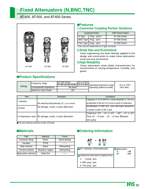
-10ç to +65ç 95% Max.
Item 1.Vibration
Time: 30 ¡ 15 max. ¡ 30 ¡ 15 max. (Minutes) 200 cycles
sMaterials
Part Connector Body Insulator Male contacts Female contacts Attenuation element Material Brass PTFE Brass Beryllium copper Metal film Finish Nickel plating
元器件交易网
Fixed Attenuators (N,BNC,TNC)
AT-400, AT-500, and AT-600 Series
sFeatures
1.Connector Coupling Portion Variations
Coupling Portion N Type BNC Type TNC Type Plug - Jackπ Plug - Jack Plug - Jack HRS Series Name AT-400 Series AT-500 Series AT-600 Series
πCan also be mated with an S type connector.
2.Small Size and Economical
Value engineering has been liberally applied to the design and construction to make these attenuators small and very economical.
- 1、下载文档前请自行甄别文档内容的完整性,平台不提供额外的编辑、内容补充、找答案等附加服务。
- 2、"仅部分预览"的文档,不可在线预览部分如存在完整性等问题,可反馈申请退款(可完整预览的文档不适用该条件!)。
- 3、如文档侵犯您的权益,请联系客服反馈,我们会尽快为您处理(人工客服工作时间:9:00-18:30)。
V 2.0
1
Байду номын сангаас
元器件交易网
Surface Mount Monolithic PIN Diode Chip Electrical Specifications @ +25°C
Symbol CT CT RS RS RS VF VR IR TL -40 Volts, 1 MHz -40 Volts, 1 GHz 10 mA, 2 MHz 2 10 mA, 100 MHz 10 mA, 1 GHz 1.0 mA 10 µA -70V 10 mA / 6 mA
DIM. A B C D E
INCHES MIN. MAX. 0.0465 0.0528 0.0173 0.0236 0.0040 0.0080 0.0150 0.0170 0.0140 0.0160
MILLIMETERS MIN. MAX. 1.180 1.340 0.440 0.600 0.102 0.203 0.381 0.432 0.355 0.406
Handling Procedures
All semiconductor chips should be handled with care to avoid damage or contamination from perspiration and skin oils. The use of plastic tipped tweezers or vacuum pickups is strongly recommended for individual components. Bulk handling should insure that abrasion and mechanical shock are minimized.
1. Exceeding these limits may cause permanent damage.
Specifications subject to change without notice. n North America: Tel. (800) 366-2266, Fax (800) 618-8883 n Asia/Pacific: Tel.+81-44-844-8296, Fax +81-44-844-8298 n Europe: Tel. +44 (1344) 869 595, Fax+44 (1344) 300 020 Visit for additional data sheets and product information.
Specifications subject to change without notice. n North America: Tel. (800) 366-2266, Fax (800) 618-8883 n Asia/Pacific: Tel.+81-44-844-8296, Fax +81-44-844-8298 n Europe: Tel. +44 (1344) 869 595, Fax+44 (1344) 300 020 Visit for additional data sheets and product information.
2, 3 2 1 1, 3
MA4SPS402 SurMount™ Series ™
Test Conditions
Units pF pF Ω Ω Ω V V µA ns
Min.
Typ. 0.034 0.041 5.0 4.6 5.0 0.84
Max. 0.045
1.00
-70
-120 10 200
1. Total capacitance is equivalent to the sum of junction capacitance C j and parasitic capacitance. 2. Series resistance RS is equivalent to the total diode series resistance including the junction resistance Rj. 3. RS and CP is measured on an HP4291A with die mounted in an ODS-186 package with conductive silver epoxy.
Rvia
Rvia
1. Rs = 2 * Rvia + Rp
+
V 2.0
2
元器件交易网
Surface Mount Monolithic PIN Diode Chip Typical Performance Curves @ +25°C
1. 2. Backside metal: 0.1 micron thk. gold. Hatched areas indicate bond pads.
Absolute Maximum Ratings1
@ T A = +25°C (unless otherwise specified)
Parameter Reverse Voltage Forward Current Operating Temperature Storage Temperature Mounting Temperature Absolute Maximum -70 V 100 mA -65°C to +150°C -65°C to +150°C +235°C for 10 seconds
元器件交易网
MA4SPS402 SurMount™ Series ™
Surface Mount Monolithic PIN Diode Chip
Features
• • • • • • • Surface Mount Diode No Wirebonds Required Rugged Silicon-Glass Construction Silicon Nitride Passivation Polymer Scratch Protection Low Parasitic Capacitance and Inductance
HSP109
C
D
E
D
D
Applications
These devices can be used in series and shunt switches up to 20 GHz where smaller area and profile are required. Low parasitic values of L and C make additional circuit tuning unnecessary. These diodes can also be used for switched pad attenuator circuits.
Rp
Cp
Bonding Techniques
Attachment to a circuit board is made simple through the use of surface mount technology. Mounting pads are conveniently located on the bottom surface of these diodes and are removed from the active junction locations. These diodes are well suited for solder attachment onto hard and soft substrates. The use of 80/20 Au/Sn and 60/40 Sn/Pb solder is recommended. Conductive epoxy paste for attachment may also be used, this can be silk-screened, or used with a conductive sheet apoxy. When soldering these diodes to a hard substrate, hot gas die bonding is preferred. We recommend utilizing a vacuum tip and a force of 60 to 100 grams applied normal to the top surface of the part. When soldering to soft substrates, it is recommended to use a lead-tin interface at the circuit board mounting pads. Position the die so that its mounting pads are aligned with the circuit board’s mounting pads Reflow the solder by heating the circuit trace near the mounting pad while applying 60 to 100 grams of force perpendicular to the top surface of the die. Since the HMIC™ glass is transparent, the edges of the mounting pads closest to each other can be visually inspected through the die after attach is completed.
High Power Handling (Efficient Heatsinking)