RYC8210-1P中文资料
chipcon smartrf cc2500单片低成本低能耗RF收发芯片 说明书

500kbps z 较低的电流消耗(RX 中 15.6mA) z 可编程控制的输出功率,可达+1dBm z 优秀的接收器选择性和模块化性能 z 极少的外部元件:芯片内频率合成器,
不需要外部滤波器或 RF 转换 z 可编程控制的基带调制解调器 z 理想的多路操作特性 z 可控的数据包处理硬件 z 快速频率变动合成器带来的合适的频
第 2 页 共 61 页
目录 1 缩写词 ....................................................................................................................... 2 2 绝对最大等级 ........................................................................................................... 5 3 工作条件 ................................................................................................................... 5 4 电气规范 ................................................................................................................... 6 5 常规特性 .....................................................................................
013 8100、8200控制屏说明

Logo
8120控制屏说明
主控制器为BE24控制器
科泰电源设备(上海)有限公司
COOLTECH POWER(SHANGHAI)LTD.
Logo
8120控制屏说明
主控制器参量信息
1、低燃油液位报警指示 2、紧急停机报警指示 3、低油压停机报警指示 4、高水温停机报警指示 5、电池电压值 6、皮带断裂/充电发电机故障报警指示 7、超/低频率停机报警指示 8、启动失败停机报警指示 9、交流发电机故障
科泰电源设备(上海)有限公司
COOLTECH POWER(SHANGHAI)LTD.
Logo
8100控制屏说明 8100控制屏(501K) 8100控制屏(501K)电路原理 控制屏
科泰电源设备(上海)有限公司
COOLTECH POWER(SHANGHAI)LTD.
Logo
8120控制屏说明
二、8120控制屏说明 8120控制屏说明
Logo
8100、8120、8200、8220控制屏说明 8100、8120、8200、8220控制屏说明
科泰电源设备(上海)有限公司
—销售服务中心
版本编号:VO.0801-13
Logo
8100、8200控制屏说明 8100、8200控制屏说明 目 录 1、8100控制屏说明 2、8120控制屏说明 3、8200控制屏说明 4、8220控制屏说明 5、KX系列ATS
科泰电源设备(上海)有限公司
COOLTECH POWER(SHANGHAI)LTD.
Logo
8120控制屏说明
控制屏外面板 1.主控制器:整个系统的主控制器; 2.微型空气开关:控制线路过流及短路保护; 3.紧急停机按钮
3
FR8210快速使用手册
FR8210 快速使用手册本文档用于对ProfiNet 适配器和FR 系列IO 模块使用的一个快速说明,阅读背景为具备一定工程经验的人员,旨在让用户能够快速上手。
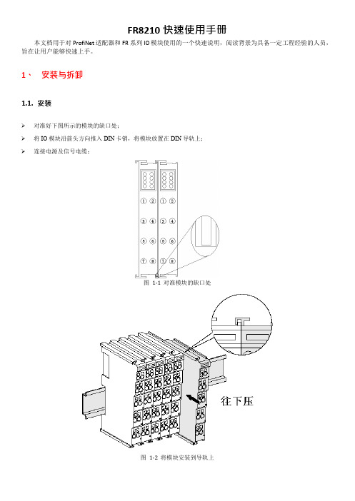
1、安装与拆卸1.1. 安装➢对准好下图所示的模块的缺口处;➢将IO 模块沿箭头方向推入DIN 卡销,将模块放置在DIN 导轨上;➢连接电源及信号电缆;图1-1 对准模块的缺口处图1-2 将模块安装到导轨上1.2. 拆卸方式➢首先应拆除本模块的所有的信号电缆或电源电缆;➢按箭头方向拉卡销(下图中的黄色部件);➢将模块取下。
图1-3 将模块从导轨上拆卸如果遇到有模块难以安装的情况,切勿使用蛮力进行安装,以免损坏当前的模块或其他模块;应当将模块从导轨上拆卸,检查模块是否存在某些异常(比如异物堵塞等),确认没有问题后,再进行插拔。
2、接线说明本文举例说明拓扑结构为FR8210-FR1108-FR2118-FR3004-FR4004 的IO 模块系统的使用说明。
2.1. 端子接线FR 系列IO 模块的接线端子采用了免螺丝设计,安装/拆卸时仅需一把一字型的螺丝刀(推荐使用一字螺丝刀的型号为2 × 75mm)即可。
推荐使用14AMG 的线,在接线过程中,先将导线剥去一定长度,再用一子型螺丝刀垂直插入端子上的孔内,向下撬动,另一只手将剥去外皮的导线插入已开启的圆形孔内,之后拔出一子型螺丝刀,导线会自动被簧片压紧。
注意不要将电源的正负极接反,否则有可能会导致模块无法工作、工作异常,甚至会导致模块损毁。
2.2. 电源接线➢如下图所示,使用一块220V-24V 的电源模块(最好是双路输出的),将电源线接好:图2-1 连接FR8210 的系统电源2.3. 系统公共端电源接线➢如下图2 所示,再将系统的公共端电源接好:注意:适配器的系统与现场测电压是通过总站和总线电源模块提供的。
适配器现场测组件是没有内部过电流保护,因此,对于这类的组件电源,必须在外部添加适当的过电流保护器件来实现过流生产,例如通过外加5A的保险丝。
BR8210 芯片数据手册 v1.02

BR8210数据手册版本1.02声明版本历史修改内容版本日期章节页码内容1.00 初始版本1.02 修订了部分章节的描述目录声明 (I)版本历史 (II)目录 (III)附图目录 (V)表格目录 (VI)缩写与术语 (VII)1介绍 (1)2主要特性 (2)3封装和引脚 (4)3.1封装形式 (4)3.2引脚分布图 (4)3.3引脚列表 (5)4功能描述 (9)4.1存储器 (9)4.1.1概述 (9)4.1.2存储器映射 (9)4.2中断 (11)4.3JTAG 调试接口 (13)4.4引导模式 (14)4.5系统控制模块(SCM) (15)4.6通用输入输出控制(GPIO) (16)4.7定时器 (17)4.8USART (18)4.8.1SPI (18)4.8.2I2C (18)4.8.3UART (19)4.9USB 从设备(Device)接口 (20)4.10USB 主从(OTG)接口 (21)4.11CMOS 光学传感器接口 (22)4.12PWM 模块 (23)4.13异步并行口(APP) (24)4.14随机数发生器(RNG) (25)5电气参数 (26)5.1极限电气参数 (26)5.2推荐运行参数 (27)5.3直流电气参数 (28)5.4片上振荡器 (29)5.5PLL (30)5.6POR (31)5.7LDO18 (32)6机械参数 (33)7 订购信息 (34)附图目录图 3-1 BR8210封装形式 (4)图 3-2 BR8210引脚分布图 (5)图 6-1 BR8210封装尺寸图 (33)表格目录表 3-1 BR8210引脚列表 (5)表 4-1 BR8210存储空间分配 (9)表 4-2 BR8210外设控制器存储空间分配 (9)表 4-3 BR8210处理器中断分配表 (12)表 4-4 BR8210引导模式 (14)表 5-1 BR8210极限电气参数 (26)表 5-2 BR8210推荐运行电气参数 (27)表 5-3 BR8210直流电气参数 (28)表 5-4 片上振荡器电气参数 (29)表 5-5 PLL电气参数 (30)表 5-6 POR电气参数 (31)表 5-7 LDO18电气参数 (32)缩写与术语JTAG:Joint Test Action Group 边界测试扫描接口SCM:System Control Module 系统控制模块GPIO:General Purpose Input/Output 通用输入输出接口USART:Universal Synchronous/Asynchronous Receiver/Transmitter 通用同步/异步收发器SPI:Serial Peripheral Interface 串行外设接口I2C:Inter-integrated CircuitUART:Universal Asynchronous Receiver/Transmitter 通用异步收发器USB:Universal Serial Bus 通用串行总线APP:Asynchronous Parallel Port Controller 异步并行接口控制器1 介绍BR8210 是一款针对嵌入式应用领域的32位MCU芯片,具有低成本、高性能、外设丰富,可靠性好的特点,基于该芯片用户可以快速的设计出符合市场需要的产品。
依米康空调操作板

依米康空调操作板中文操作电脑板用户指南依米康空调设备有限公司机组简介依米康空调设备由意大利EMICON公司生产,这是一家致力于环境处理的专业生产公司,其产品荣获ISO9001国际认证。
其中的ED系列空调是一种恒温恒湿专用空调,它以365天×24小时的优异工作状态对专用机房的环境作精确的处理、控制,可以在温度12-32℃、±1℃,湿度30-80%、±2%的范围所有设定及告警为中文显示,方便操作和管理。
2.涡旋式压缩机噪音低、效率高、寿命长、全封闭不易漏、重量轻。
3.风机布置独特所有的风机均设计位于机组的中部,有利降噪。
4.储液罐保证了膨胀阀的均匀工作,系统稳定性提高,使温度控制更加精确,冬天可以可靠运行。
5.室外机抗腐蚀设计,有静音型可选,运行温度范围-35℃~46℃。
标准型噪音为47-54dBA, 静音型为35-49 dBA。
马达转速可调。
6.监控接口同一场地可监控254台机组,可提供通讯协议及监控软件。
7.加热器电极式加热,带热保护装置(自动复位)及护罩。
8.整机体积小,重量轻,省电,有新风口设计(选件)。
机组为正面维护设计,检修时不用停机。
二、主要部件1.压缩机康普兰(Copeland)涡旋式压缩机。
高效、省电、低噪。
例:消耗1KW电功率,活塞式可产生2.9KW制冷功率,60dBA。
涡旋式可产生3.4KW制冷功率,54dBA。
2.膨胀阀大机组为斯坡兰(sporlan),美国生产。
小机组为丹佛斯(Danfoss),丹麦生产。
热力式膨胀阀,控制精密,可调节。
3.室外机电机为德国ZHIEL Abey(依必安),质量可靠,可调速,外置转子,有利散热。
4.蒸发器、冷凝器由意大利生产,工艺精美,抗腐蚀设计。
5.电脑板、加热器、加湿器、室内风机意大利专业厂家生产,质量可靠,操作维护简易,保护可靠。
2电脑板按键介绍-1- 每个键旁的绿色指示灯表明这个键已被选中,只要这个屏在使用,指示灯就保持在“on”上。
NSi812x高可靠双通道数字隔离器数据手册说明书
C O NF ID EN T IA LNSi8120/NSi8121/NSi8122: High ReliabilityDual-Channel Digital IsolatorsDatasheet (EN) 1.8Product OverviewThe NSi812x devices are high reliability dual-channel digital isolator. The NSi812x device is safety certified by UL1577 support several insulation withstand voltages (3.75kV rms , 5kV rms ), while providing high electromagnetic immunity and low emissions at low power consumption. The data rate of the NSi812x is up to 150Mbps, and the common-mode transient immunity (CMTI) is up to 150kV/us. The NSi812x device provides digital channel direction configuration and the default output level configuration when the input power is lost. Wide supply voltage of the NSi812x device support to connect with most digital interface directly, easy to do the level shift. High system level EMC performance enhance reliability and stability of use. AEC-Q100 (Grade 1) option is provided for all devices.Key Features• Up to 5000V rms Insulation voltage• Date rate: DC to 150Mbps• Power supply voltage: 2.5V to 5.5V • All devices are AEC-Q100 qualified • High CMTI: 150kV/us • Chip level ESD: HBM: ±6kV• High system level EMC performance:Enhanced system level ESD, EFT, Surge immunity• Default output high level or low level option • Isolation barrier life: >60 years• Low power consumption: 1.5mA/ch (1 Mbps) • Low propagation delay: <15ns • Operation temperature: -40℃~125℃ • RoHS-compliant packages:SOIC-8 narrow body SOIC-16 wide bodySafety Regulatory Approvals• UL recognition: up to 5000V rms for 1 minute per UL1577• CQC certification per GB4943.1-2011• CSA component notice 5A • DIN VDE V 0884-11:2017-01Applications• Industrial automation system • Isolated SPI, RS232, RS485• General-purpose multichannel isolation • Motor controlFunctional Block DiagramsC O NF ID EN T IA LIndex1.0 ABSOLUTE MAXIMUM RATINGS .............................................................................................................................. 3 2.0 SPECIFICATIONS ........................................................................................................................................................... 3 2.1. E LECTRICAL CHARACTERISTICS .................................................................................................................................................. 3 2.2. TYPICAL PERFORMANCE CHARACTERISTICS ........................................................................................................................... 7 2.3. P ARAMETER M EASUREMENT I NFORMATION . (8)3.0 HIGH VOLTAGE FEATURE DESCRIPTION (9)3.1. INSULATION AND SAFETY RELATED SPECIFICATIONS (9)3.2. DIN VDE V 0884-11(VDE V 0884-11):2017-01 INSULATION CHARATERISTICS ....................................................................... 9 3.3. R EGULATORY INFORMATION ................................................................................................................................................... 11 4.0 FUNCTION DESCRIPTION ..........................................................................................................................................11 5.0 APPLICATION NOTE ................................................................................................................................................... 12 5.1. PCB L AYOUT ...................................................................................................................................................................... 12 5.2. H IGH SPEED PERFORMANCE ................................................................................................................................................... 12 5.3. T YPICAL S UPPLY C URRENT E QUATIONS ..................................................................................................................................... 13 6.0 PACKAGE INFORMATION ......................................................................................................................................... 13 7.0 TAPE AND REEL INFORMATION ............................................................................................................................. 17 8.0 ORDER INFORMATION .............................................................................................................................................. 20 9.0 REVISION HISTORY . (21)C O NF ID EN T IA L1.0 ABSOLUTE MAXIMUM RATINGSPower Supply Voltage VDD1, VDD2 -0.5 6.5 V Maximum Input Voltage VINA, VINB -0.4 VDD+0.41 V Maximum Output Voltage V OUTA , V OUTB -0.4 VDD+0.41 VMaximum Input/Output Pulse VoltageVINA, VINB, V OUTA , V OUTB-0.8VDD+0.8VPulse width should be less than 100ns, and the duty cycle should be less than 10%Common-Mode Transients CMTI ±150 kV/us Output currentIo -15 15mAMaximum Surge Isolation VoltageV IOSM5.3kVOperating Temperature Topr -40125 ℃Storage Temperature Tstg -40150℃Electrostatic dischargeHBM±6000VCDM±2000V1 The maximum voltage must not exceed 6.5V.2.0 SPECIFICATIONS2.1. ELECTRICAL CHARACTERISTICS(VDD1=2.5V~5.5V, VDD2=2.5V~5.5V, Ta=-40℃ to 125℃. Unless otherwise noted, Typical values are at VDD1 = 5V, VDD2 = 5V, Ta =25℃)Power on ResetVDD POR2.2 V POR threshold as during power-upVDD HYS 0.1 V POR threshold Hysteresis Input ThresholdV IT1.6 V Input Threshold at rising edge V IT_HYS 0.4 V Input Threshold Hysteresis High Level Input Voltage V IH 2 V Low Level Input Voltage V IL 0.8 V High Level Output Voltage V OH VDD-0.3 V I OH ≤ 4mA Low Level Output VoltageV OL0.3VI OL ≤ 4mAC O NF ID EN T IA LOutput Impedance R out 50 ohm Input Pull high or low CurrentI pull 8 15 uA Start Up Time after POR trbs 40 usec Common Mode Transient ImmunityCMTI±100±150kV/us(VDD1=5V± 10%, VDD2=5V± 10%, Ta=-40℃ to 125℃. Unless otherwise noted, Typical values are at VDD1 = 5V, VDD2 = 5V, Ta = 25℃)Supply currentNSi8120 I DD1(Q0) 0.58 0.87 mAAll Input 0V for NSi8120x0 Or All Input at supply for NSi8120x1 I DD2(Q0) 1.18 1.77 mA I DD1(Q1) 2.92 4.38 mA All Input at supply for NSi8120x0 Or All Input 0V for NSi8120x1I DD2(Q1) 1.241.86mAI DD1(1M) 1.71 2.56 mA All Input with 1Mbps, C L =15pFI DD2(1M)1.382.07mAI DD1(10M) 1.78 2.67 mA All Input with 10Mbps, C L =15pF I DD2(10M)3.24.8mA I DD1(100M)2.103.15 mA All Input with 100Mbps, C L =15pFI DD2(100M)21.031.5mANSi8121/ NSi8122 I DD1(Q0) 1.031.55 mA All Input 0V for NSi812xx0 Or All Input at supply for NSi812xx1 I DD2(Q0) 1.00 1.5 mA I DD1(Q1)2.203.3 mA All Input at supply for NSi812xx0Or All Input 0V for NSi812xx1 I DD2(Q1)2.133.2 mA I DD1(1M) 1.72 2.58 mA All Input with 1Mbps, C L =15pFI DD2(1M) 1.68 2.52 mA I DD1(10M) 2.62 3.93 mA All Input with 10Mbps, C L =15pFI DD2(10M) 2.71 4.06 mA I DD1(100M) 11.01 16.5 mA All Input with 100Mbps, C L = 15pF I DD2(100M)12.8 19.2 mA Data RateDR 0 150 MbpsC O NF ID EN T IA LPropagation Delayt PLH 5 8.20 15 ns See Figure 2.7 , C L = 15pF t PHL 5 10.56 15 ns See Figure 2.7, C L = 15pF Pulse Width Distortion |t PHL – t PLH | PWD5.0nsSee Figure 2.7 , C L = 15pFRising Time t r 5.0 ns See Figure 2.7 , C L = 15pF Falling Timet f 5.0 ns See Figure 2.7 , C L = 15pFPeak Eye Diagram Jitter t JIT (PK) 350 ps Channel-to-Channel Delay Skewt SK (c2c) 2.5 nsPart-to-Part Delay Skewt SK (p2p)5.0ns(VDD1=3.3V± 10%, VDD2=3.3V± 10%, Ta=-40℃ to 125℃. Unless otherwise noted, Typical values are at VDD1 = 3.3V, VDD2 = 3.3V, Ta =25℃)Supply currentNSi8120 I DD1(Q0) 0.550.83mA All Input 0V for NSi8120x0 Or All Input at supply for NSi8120x1 I DD2(Q0) 1.12 1.68 mA I DD1(Q1) 2.87 4.3 mA All Input at supply for NSi8120x0 Or All Input 0V for NSi8120x1 I DD2(Q1)1.18 1.77mA I DD1(1M)1.72.55mA All Input with 1Mbps, C L = 15pFI DD2(1M)1.271.91 mA I DD1(10M) 1.732.6 mA All Input with 10Mbps, C L = 15pF I DD2(10M)2.413.6 mA I DD1(100M) 2.05 3.08 mA All Input with 100Mbps, C L = 15pF I DD2(100M)14.0521.08mANSi8121/ NSi8122 I DD1(Q0) 0.98 1.47 mA All Input 0V for NSi812xx0 Or All Input at supply for NSi812xx1 I DD2(Q0) 0.95 1.43 mA I DD1(Q1) 2.14 3.21 mA All Input at supply for NSi812xx0 Or All Input 0V for NSi812xx1 I DD2(Q1) 2.08 3.12 mA I DD1(1M) 1.63 2.45 mA All Input with 1Mbps, C L = 15pFI DD2(1M) 1.59 2.39 mA I (10M)2.223.33mAAll Input with 10Mbps,C O NF I D EN T IA LI DD2(10M) 2.25 3.38 mA C L = 15pFI DD1(100M) 7.57 11.36 mA All Input with 100Mbps, C L = 15pF I DD2(100M)8.5 12.75 mA Data RateDR 0 150 Mbps Minimum Pulse Width PW 5.0 nsPropagation Delayt PLH 5 9.20 15 ns See Figure 2.7 , C L = 15pF t PHL5 10.40 15 ns See Figure 2.7, C L = 15pF Pulse Width Distortion |t PHL – t PLH | PWD5.0nsSee Figure 2.7 , C L = 15pFRising Time t r 5.0 ns See Figure 2.7 , C L = 15pF Falling Timet f5.0 nsSee Figure 2.7 , C L = 15pFPeak Eye Diagram Jitter t JIT (PK) 350psChannel-to-Channel Delay Skewt SK (c2c)2.5nsPart-to-Part Delay Skew t SK (p2p)5.0ns(VDD1=2.5V± 10%, VDD2=2.5V± 10%, Ta=-40℃ to 125℃. Unless otherwise noted, Typical values are at VDD1 = 2.5V, VDD2 = 2.5V, Ta =25℃)Supply currentNSi8120I DD1(Q0) 0.53 0.8 mA All Input 0V for NSi8120x0 Or All Input at supply for NSi8120x1 I DD2(Q0) 1.11.65 mA I DD1(Q1)2.85 4.28 mA All Input at supply for NSi8120x0 Or All Input 0V for NSi8120x1 I DD2(Q1)1.15 1.73 mA I DD1(1M) 1.632.45 mA All Input with 1Mbps, C L = 15pFI DD2(1M) 1.21 1.82 mA I DD1(10M) 1.68 2.52 mA All Input with 10Mbps, C L = 15pFI DD2(10M) 2.05 3.08 mA I DD1(100M) 1.95 2.93 mA All Input with 100Mbps, C L = 15pFI DD2(100M)10.415.6mANSi8121/ NSi8122I DD1(Q0) 0.96 1.44 mA All Input 0V for NSi812xx0 Or All Input at supply for NSi812xx1I (Q0)0.931.395mAF ID EN T IA LI DD1(Q1) 2.11 3.165 mA All Input at supply for NSi812xx0Or All Input 0V for NSi812xx1 I DD2(Q1) 2.05 3.075 mA I DD1(1M) 1.58 2.37 mA All Input with 1Mbps, C L = 15pFI DD2(1M) 1.54 2.31 mA I DD1(10M) 2.02 3.03 mA All Input with 10Mbps, C L = 15pFI DD2(10M) 2.04 3.06 mA I DD1(100M) 6.03 9.045 mA All Input with 100Mbps, C L = 15pF I DD2(100M)6 9 mAData RateDR 0 150 Mbps Minimum Pulse Width PW 5.0 nsPropagation Delayt PLH 5 10 15 nsSee Figure 2.7 , C L = 15pF t PHL5 10 15nsSee Figure 2.7, C L = 15pFPulse Width Distortion |t PHL – t PLH | PWD5.0nsSee Figure 2.7 , C L = 15pFRising Time t r5.0ns See Figure 2.7 , C L = 15pF Falling Timet f5.0 ns See Figure 2.7 , C L = 15pFPeak Eye Diagram Jitter t JIT (PK)350ps Channel-to-Channel Delay Skewt SK (c2c)2.5ns Part-to-Part Delay Skew t SK (p2p)5.0ns2.2. TYPICAL PERFORMANCE CHARACTERISTICSFigure 2.1 NSi8120 VDD1 Supply Current vs Data Rate Figure 2.2 NSi8120 VDD2 Supply Current vs Data RateC OE2.3. PARAMETER MEASUREMENT INFORMATIONC LFigure 2.7 Switching Characteristics Test Circuit and WaveformFigure 2.8 Common-Mode Transient Immunity Test CircuitC O NF ID EN T IA L3.0 HIGH VOLTAGE FEATURE DESCRIPTION3.1. INSULATION AND SAFETY RELATED SPECIFICATIONSMinimum External Air Gap (Clearance)L(I01) 4.0 8.0 mm Shortest terminal-to-terminal distance through air Minimum External Tracking (Creepage)L(I02)4.08.0mmShortest terminal-to-terminal distance across the package surfaceMinimum internal gap DTI 20 um Distance through insulationTrackingResistance(Comparative Tracking Index) CTI>400VDIN EN 60112 (VDE 0303-11); IEC 60112Material GroupⅡ3.2. DIN VDE V 0884-11(VDE V 0884-11):2017-01 INSULATION CHARATERISTICSSOIC-8 SOIC-16 Installation Classification per DIN VDE 0110For Rated Mains Voltage ≤ 150V rms Ⅰto Ⅳ Ⅰto Ⅳ For Rated Mains Voltage ≤ 300V rms Ⅰto Ⅲ Ⅰto Ⅳ For Rated Mains Voltage ≤ 400V rms Ⅰto Ⅲ Ⅰto Ⅳ Climatic Classification10/105/2110/105/21 Pollution Degree per DIN VDE 0110, Table 122Maximum repetitive isolation voltageVIORM 565 849 Vpeak Input to Output Test Voltage, Method B1V IORM × 1.5 = V pd (m) , 100%production test, t ini = t m = 1 sec, partial discharge < 5 pCV pd (m)8471273VpeakInput to Output Test Voltage, Method AAfter Environmental Tests Subgroup 1V IORM × 1.2= V pd (m) , t ini = 60 sec, t m = 10 sec, partial V pd (m)6781018VpeakC O N T IA LAfter Input and /or Safety Test Subgroup 2 and Subgroup 3 V IORM × 1.2= V pd (m) , t ini = 60 sec, t m = 10 sec, partialdischarge < 5 pC V pd (m)6781018VpeakMaximum transient isolation voltage t = 60 sec VIOTM 5300 7000 Vpeak Maximum Surge Isolation VoltageTest method per IEC60065,1.2/50uswaveform, VTEST=VIOSM×1.3VIOSM53845384VpeakIsolation resistance VIO =500V RIO >109 >109 Ω Isolation capacitance f = 1MHzCIO 0.6 0.6pFInput capacitanceCI22pF Total Power Dissipation at 25℃Ps1499 mW Safety input, output, or supply currentθJA = 140 °C/W, V I = 5.5 V, T J = 150 °C, T A = 25 °C Is160mAθJA = 84 °C/W, V I = 5.5 V, T J = 150 °C, T A = 25 °C237 mA Case TemperatureTs150150℃Figure 3.2 NSi8120W/NSi8121W/NSi8122W Thermal Derating Curve, Dependence of Safety Limiting Values with Case Temperature per DIN VDE V 0884-11C O NF ID EN T IA L3.3. REGULATORY INFORMATIONThe NSi8120N/NSi8121N/NSi8122N are approved by the organizations listed in table.UL 1577 Component Recognition Program 1Approved under CSA ComponentAcceptance Notice 5ADIN VDE V 0884-11:2017-012Certified by CQC11-471543-2012 GB4943.1-2011Single Protection, 3750V rms Isolation voltageSingle Protection, 3750V rms IsolationvoltageBasic Insulation 565Vpeak, V IOSM =5384VpeakBasic insulation at 400V rms (565Vpeak)File (E500602)File (E500602)File (5024579-4880-0001)File (pending)1 In accordance with UL 1577, each NSi8120N/NSi8121N/NSi8122N is proof tested by applying an insulation test voltage ≥ 4500 Vrms for 1 sec.2 In accordance with DIN VDE V 0884-11, each NSi8120N/NSi8121N/NSi8122N is proof tested by applying an insulation test voltage ≥ 847 V peak for 1 sec(partial discharge detection limit = 5 pC). The * marking branded on the component designates DIN VDE V 0884-11 approval.The NSi8120W/NSi8121W/NSi8122W are approved by the organizations listed in table.UL 1577 Component Recognition Program 1Approved under CSAComponent Acceptance Notice5ADIN VDE V 0884-11(VDE V 0884-11):2017-012 Certified by CQC11-471543-2012 GB4943.1-2011Single Protection, 5000V rms Isolation voltageSingle Protection, 5000V rmsIsolation voltageBasic Insulation 849Vpeak, V IOSM =5384Vpeak Basic insulation at 800V rms (1131Vpeak) Reinforced insulation at 400V rms (565Vpeak)File (E500602)File (E500602)File (5024579-4880-0001)File (pending)1 In accordance with UL 1577, each NSi8120W/NSi8121W/NSi8122W is proof tested by applying an insulation test voltage ≥ 6000 V rms for 1 sec.2 In accordance with DIN VDE V 0884-11, each NSi8120W/NSi8121W/NSi8122W is proof tested by applying an insulation test voltage ≥ 1273 V peak for 1 sec(partial discharge detection limit = 5 pC). The * marking branded on the component designates DIN VDE V 0884-11 approval.4.0 FUNCTION DESCRIPTIONThe NSi812x is a Dual-channel digital isolator based on a capacitive isolation barrier technique. The digital signal is modulated with RF carrier generated by the internal oscillator at the Transmitter side. Then it is transferred through the capacitive isolation barrier and demodulated at the Receiver side.The NSi812x devices are high reliability dual-channel digital isolator with AEC-Q100 qualified. The NSi812x device is safety certified by UL1577 support several insulation withstand voltages (3.75kV rms , 5kV rms ), while providing high electromagnetic immunity and low emissions at low power consumption. The data rate of the NSi812x is up to 150Mbps, and the common-mode transient immunity (CMTI) is up to 150kV/us. The NSi812x device provides digital channel direction configuration and the default output level configuration when the input power is lost. Wide supply voltage of the NSi812x device support to connect with most digital interface directly, easy to do the level shift. High system level EMC performance enhance reliability and stability of use.The NSi812x has a default output status when VDDIN is unready and VDDOUT is ready as shown in Table 4.1, which helps for diagnosis when power is missing at the transmitter side. The output B follows the same status with the input A within 1us after powering up.C O NF ID EN T IA LCopyright © 2019, NOVOSENSEPage 12 Table 4.1 Output status vs. power statusH Ready Ready H Normal operation.L Ready Ready L XUnreadyReadyL HThe output follows the same status with the input within 60us after input side VDD1 is powered on.X Ready Unready XThe output follows the same status with the input within 60us after output side VDD2 is powered on.5.0 APPLICATION NOTE5.1. PCB LAYOUTThe NSi812x requires a 0.1 µF bypass capacitor between VDD1 and GND1, VDD2 and GND2. The capacitor should beplaced as close as possible to the package. Figure 5.1 to Figure 5.4 show the recommended PCB layout, make sure the space under the chip should keep free from planes, traces, pads and via. To enhance the robustness of a design, the user may also include resistors (50–300 Ω ) in series with the inputs and outputs if the system is excessively noisy. The series resistors also improve the system reliability such as latch-up immunity.The typical output impedance of an isolator driver channel is approximately 50 Ω, ±40%. When driving loads where transmission line effects will be a factor, output pins should be appropriately terminated with controlled impedance PCB traces.Figure5.1 Recommended PCB Layout — Top Layer Figure5.2 Recommended PCB Layout — Bottom LayerFigure5.3 Recommended PCB Layout — Top Layer Figure5.4 Recommended PCB Layout — Bottom Layer5.2. HIGH SPEED PERFORMANCEFigure 5.5 shows the eye diagram of NSi812x at 200Mbps data rate output. The result shows a typical measurement on the NSi812x with 350ps p-p jitter.C O NF ID EN T IA LFigure5.5 NSi812x Eye Diagram5.3. TYPICAL SUPPLY CURRENT EQUATIONSThe typical supply current of NSi812x can be calculated using below equations. I DD1 and I DD2 are typical supply currents measured in mA, f is data rate measured in Mbps, C L is the capacitive load measured in pFNSi8120:I DD1 = 0.19 *a1+1.45*b1+0.82*c1. I DD2 = 1.36+ VDD1*f* C L *c1*10-9When a1 is the channel number of low input at side 1, b1 is the channel number of high input at side 1, c1 is the channel number of switch signal input at side 1.NSi8121/ NSi8122:I DD1 = 0.87 +1.26*b1+0.63*c1+ VDD1*f* C L *c2*10-9I DD2 = 0.87 +1.26*b2+0.63*c2+ VDD1*f* C L *c1*10-9When b1 is the channel number of high input at side 1, c1 is the channel number of switch signal input at side 1, b2 is the channel number of high input at side 2, c2 is the channel number of switch signal input at side 2.6.0 PACKAGE INFORMATIONVDD GND 22VDD INA GND 2VDD 2Figure 6.1 NSi8120N Package Figure 6.2 NSi8121N PackageC O NF ID EN T IA LVDD INBGND 22Figure 6.3 NSi8122N PackageFigure 6.4 SOIC8 Package Shape and Dimension in millimeters (inches)Table6.1 NSi8120N/ NSi8121N/ NSi8122N Pin Configuration and DescriptionNSi8121N PIN NO.NSi8122N PIN NO.SYMBOL FUNCTION1 1 1 VDD1 Power Supply for Isolator Side 12 7 2 INA Logic Input A3 3 6 INB Logic Input B4 4 4 GND1 Ground 1, the ground reference for Isolator Side 15 5 5 GND2 Ground 2, the ground reference for Isolator Side 26 6 3 OUTB Logic Output B7 2 7 OUTA Logic Output A888VDD2Power Supply for Isolator Side 2C O NFVDD GND GND 2VDD 2GND 2GND NC NCNC VDD GND GND 2VDD 22GND NC NC NCFigure 6.5 NSi8120W Package Figure 6.6 NSi8121W PackageVDD INB GND GND 2VDD 2GND 2GND NC NC NCFigure 6.7 NSi8122W PackageFigure 6.8 WB SOIC16 Package Shape and Dimension in millimeters and (inches)C O NF ID EN T IA LTable 6.2 NSi8120W/ NSi8121W/ NSi8122W Pin Configuration and Description1 1 1 GND1 Ground 1, the ground reference for Isolator Side 12 2 2 NC No Connection.3 3 3 VDD1 Power Supply for Isolator Side 14 13 4 INA Logic Input A5 5 12 INB Logic Input B6 6 6 NC No Connection.7 7 7 GND1 Ground 1, the ground reference for Isolator Side 18 8 8 NC No Connection. 9 9 9 GND2 Ground 2, the ground reference for Isolator Side 210 10 10 NC No Connection. 11 11 11 NC No Connection. 12 12 5OUTB Logic Output A 13 4 13OUTALogic Output B 14 14 14 VDD2 Power Supply for Isolator Side 215 15 15 NC No Connection.161616GND2Ground 2, the ground reference for Isolator Side 27.0TAPE AND REEL INFORMATIONLAITNEDIFNOCC O NF ID EN T IA LFigure 7.1 Tape and Reel Information of SOIC8LAITNEDIFNOCFigure 7.2 Tape and Reel Information of WB SOIC16NF ID EN T IA L8.0 ORDER INFORMATIONNSi8120N0 3.75 2 0 150 Low -40 to 125℃ NO SOIC8 NSi8120N1 3.75 2 0 150 High -40 to 125℃ NO SOIC8 NSi8121N0 3.75 1 1 150 Low -40 to 125℃ NO SOIC8 NSi8121N1 3.75 1 1 150 High -40 to 125℃ NO SOIC8 NSi8122N0 3.75 1 1 150 Low -40 to 125℃ NO SOIC8 NSi8122N1 3.75 1 1 150 High -40 to 125℃ NO SOIC8 NSi8120W0 5 2 0 150 Low -40 to 125℃ NO WB SOIC16 NSi8120W1 5 2 0 150 High -40 to 125℃ NO WB SOIC16 NSi8121W0 5 1 1 150 Low -40 to 125℃ NO WB SOIC16 NSi8121W1 5 1 1 150 High -40 to 125℃ NO WB SOIC16 NSi8122W0 5 1 1 150 Low -40 to 125℃ NO WB SOIC16 NSi8122W1 5 1 1 150 High -40 to 125℃ NO WB SOIC16 NSi8120N0Q 3.75 2 0 150 Low -40 to 125℃ YES SOIC8 NSi8120N1Q 3.75 2 0 150 High -40 to 125℃ YES SOIC8 NSi8121N0Q 3.75 1 1 150 Low -40 to 125℃ YES SOIC8 NSi8121N1Q 3.75 1 1 150 High -40 to 125℃ YES SOIC8 NSi8122N0Q 3.75 1 1 150 Low -40 to 125℃ YES SOIC8 NSi8122N1Q 3.75 1 1 150 High -40 to 125℃ YES SOIC8 NSi8120W0Q 5 2 0 150 Low -40 to 125℃ YES WB SOIC16 NSi8120W1Q 5 2 0 150 High -40 to 125℃ YES WB SOIC16 NSi8121W0Q 5 1 1 150 Low -40 to 125℃ YES WB SOIC16 NSi8121W1Q 5 1 1 150 High -40 to 125℃ YES WB SOIC16 NSi8122W0Q 5 1 1 150 Low -40 to 125℃ YES WB SOIC16 NSi8122W1Q 5 1 1 150 High -40 to 125℃YES WB SOIC16 NOTE: All packages are RoHS-compliant with peak reflow temperatures of 260 °C according to the JEDEC industry standard classifications and peak solder temperatures. All devices are AEC-Q100 qualified.Part Number Rule:NSi(81)(2)(1)(N)(1)(Q)C O NF ID EN T IA LNSi8120/NSi8121/NSi81229.0 REVISION HISTORY1.0 Original2017/11/15 1.1 Change to Ordering information2018/3/26 1.2 Add maximum operation current specification. 2018/6/20 1.3 Change block diagram 2018/7/28 1.4 Correct Table 6.2 Pin No.2018/8/20 1.5 Add specification “Input Pull high or low Current” 2018/9/10 1.6 Add “Maximum Input/Output Pulse Voltage” 2018/10/91.7 Change to Ordering information 2018/12/20 1.8 Change Certification Information2019/06/17。
KTY84-150温度传感器中文资料,KTY84温度传感器中文资料
南京华巨电子有限公司Sinochip(Nanjing)Electronics Co.,LTDSKTY84‐150硅温度传感器中文资料 KTY84温度传感器中文资料产 品 规 格 书文件编号 Q/SC.G-49.07.031-2015产品名称 KTY84-150温度传感器, KTY84/150温度传感器产品代码 49007031产品型号 SKTY84-150-S2(520)版 次 A/0拟制: 王立志审核: 张建军批准: 唐成刚2015年11月27日发布 2015年11月27日实施1、产品名称、型号、代码、型号规则 (2)2、主要参数2.1产品执行标准 (2)2.2外形尺寸,结构 (2)2.3性能参数 (3)2.4温度特性曲线图 (3)2.5S Y84-150分度表 (4)3、包装 (5)1、产品名称、型号、代码、型号规则名称:硅温度传感器型号:SKTY84-150-S2(520)代码:49011027型号规则:2、主要参数2.1产品执行标准IEC601342.2外形尺寸、结构Q/SC.G-49.11.027-2015版次: A/0 共 5 页 第 3 页 2.3 性能参数序号 项目 技术要求1 常温电阻(R25℃) 603±38Ω2 100摄氏度电阻(R100℃) 1000±50Ω3 温度系数(100℃) 0.61%K4 温度范围(压接式) -40℃~210℃5 标准工作电流 2mA6 最大工作电流(环境温度25℃) 10mA(max)7 热动作时间(τ) 在静止空气中τ=20s 在静止液体中τ=1s 在流动液体中τ=0.5s(注:热动作时间τ是传感器的环境对应的阻值,要上升到某一温度的度数。
63.2%转移到环境温度所用的时间。
)2.4温度特性曲线图Q/SC.G-49.11.027-2015版次: A/0 共 5 页 第 4 页 2.5 KTY84-150分度表R-T特性参数表摄氏度华氏度KTY84-150℃℉ %/(K)(Ω)(K)MIN TYP MAX‐40 ‐40 0.84 332 359 386 ±8.85 ‐30 ‐22 0.83 362 391 419 ±8.76 ‐20 ‐4 0.82 394 424 455 ±8.70 ‐10 14 0.80 428 460 492 ±8.65 0 32 0.79 464 498 532 ±8.61 10 50 0.77 503 538 574 ±8.58 20 68 0.75 544 581 618 ±8.55 25 77 0.74 565 603 641 ±8.54 30 88 0.73 587 626 665 ±8.53 40 104 0.71 632 672 713 ±8.50 50 122 0.70 679 722 764 ±8.46 60 140 0.68 729 773 817 ±8.42 70 158 0.66 781 826 872 ±8.37 80 176 0.64 835 882 929 ±8.31 90 194 0.63 891 940 989 ±8.25 100 212 0.61 950 1000 1050 ±8.17 110 230 0.60 1007 1062 1117 ±8.66 120 248 0.58 1067 1127 1187 ±9.17 130 266 0.57 1128 1194 1259 ±9.69 140 284 0.55 1191 1262 1334 ±10.24 150 302 0.54 1256 1334 1412 ±10.80 160 320 0.53 1322 1407 1492 ±11.37 170 338 0.52 1391 1482 1574 ±11.96 180 356 0.51 1461 1560 1659 ±12.58 190 374 0.49 1533 1640 1747 ±13.20 200 392 0.48 1607 1722 1837 ±13.85 210 410 0.47 1863 1807 1931 ±14.51Q/SC.G-49.11.027-2015版次: A/0 共 5 页 第 4 页 温度特性曲线图3、包装产品放入塑料袋内,并放入质检证后塑封;包装箱内附有检验报告、送货单。
BGK-FBG-8210便携式解调仪使用手册中文
FBG8210 便携式解调仪 使用手册
北京基康科技有限公司
1998-2008 (C) All rights reserved. Page 1/73
BGK-FBG8210 便携式解调仪使用手册
图片:BGK-FBG-8210 便携式解调仪
1998-2008 (C) All rights reserved. Page 2/73
1998-2008 (C) All rights reserved. Page 4/73
BGK-FBG8210 便携式解调仪使用手册
1. 概述
光纤传感技术是 20 世纪 70 年代伴随光通信技术的发展而迅速发展起来的一种新型传 感技术。作为被测信号载体的光波和作为光波传播媒介的光纤,具有一系列独特的、其他 载体和媒介难以比拟的优点:光纤本身不带电、体积小、质量轻、易弯曲、抗电磁干扰、 抗辐射性能好,特别适用于易燃、易爆、空间受严格限制和强电磁场等恶劣环境下使用。
6.3 数据的测量及存储 ............................................................... 40 6.3.1 连续自动测量工作模式时的测量及存储..........................................40 6.3.2 单次手动测量工作模式时的测量及存储..........................................41 6.3.3 测量过程中出现的测量故障....................................................42
WARNING:使用时请保持仪器的稳定。 CAUTION:请不要将本仪器直接置于下雨或太潮湿的环境中。
- 1、下载文档前请自行甄别文档内容的完整性,平台不提供额外的编辑、内容补充、找答案等附加服务。
- 2、"仅部分预览"的文档,不可在线预览部分如存在完整性等问题,可反馈申请退款(可完整预览的文档不适用该条件!)。
- 3、如文档侵犯您的权益,请联系客服反馈,我们会尽快为您处理(人工客服工作时间:9:00-18:30)。
Fax: 800-227-4866Devices PAGE NO.: 1 OF 2Specification Status: ReleasedABSOLUTE MAXIMUM RATINGS (Note 1)Parameter Symbol Value UnitsMax supply voltage V IN +8 VFault flag voltage V FLG +8 VFault flag current I FLG 50 µAOutput voltage V OUT +8 Vlimited AOutput current I OUT InternallyControl input V EN− 0.3 to +12.0 VStorage temperature T S− 65 to +150 °CMax lead temperature during soldering (5 sec.) 260 °COPERATING RATINGS (Note 3)Parameter Symbol Value Units+5.5 VtoSupply voltage V IN +3Continuous output current (each output) I OUT 0.6 A+85 °CtoAmbient operating temperature T A -40Thermal resistance (DIP-8) θJ A120 °C/WELECTRICAL CHARACTERISTICS (V IN = +5V; T A = 25°C; unless noted.)Power switch Condition Min Typ Max UnitsSwitch Resistance V IN = 5V, I OUT = 500mA, each switch 95 120 mΩV IN = 3.3V, I OUT = 500mA, each switch 90 110 mΩOutput Turn-On Time R L = 10Ωeach output, consists of delay+rise time 3.6 12 msOutput Turn-Off Time R L = 10Ωeach output, consists of delay+fall time 2 40 µsCurrent limit Condition Min Typ Max UnitsShort-Circuit Current Limit Each output (enable into 0Ωload) 0.6 0.9 1.25 AEach output (3Ωload hot-plugged into EN device), V OUT = 4.0V 0.6 0.9 1.25 AEnable input Condition Min Typ Max UnitsEnable Input Threshold Low-to-high transition 1.5 2.4 VHigh-to-low transition, Note 4 0.8 1.5 VEnable Input Current V EN = 0V to 5.5V 0.01 1 µAEnable Input Capacitance 5 pFSupply current Condition Min Typ Max Units50.5 Supply Current Switch off, OUT = open; Note4µASwitches on, OUT = open; Note4 200 250 µAOutput Leakage Current Each output (output disabled) 10 µAOT, UVLO/OVLO Condition Min Typ Max UnitsOvertemperature Shutdown T J increasing 135 CThreshold T J decreasing 125 CUVLO Threshold V IN = increasing 2.5 VV IN = decreasing 2.3 VOVLO Threshold V IN = increasing 6.4 VV IN = decreasing 6.1 VError flag Condition Min Typ Max UnitsError Flag Output Resistance V IN = 5V, I L = 10µA, Note 5 50 100 ΩV IN = 3.3V, I L = 10µA, Note 5 80 100 ΩError flag output delay Fault on overcurrent, Note 6 6 9 15 msError Flag Off Current V FLAG = 5V 0.01 1 µAFax: 800-227-4866DevicesPAGE NO.: 2 OF 2ELECTRICAL CHARACTERISTICS - NOTESNote 1. Exceeding the absolute maximum rating may damage the device. Note 2. Devices are ESD sensitive. Handling precautions recommended. Note 3. The device is not designed to function outside its operating rating.Note 4. Off is ≤ 0.8V and on is ≥ 2.4V for the RYC8220-1 and RYC8220-3. Off is ≥ 2.4V and on is ≤ 0.8V for the RYC8220-2 and RYC8220-4. Theenable input has approximately 200mV of hysteresis. Pull-down/Pull-up resistors are on chip for “-1” and “-2” configurations.Note 5. Pull-up resistors are on chip.Note 6. No error flag out delay on UVLO, OVLO, and thermal shut down.PIN CONFIGURATION: DEVICE MARKING:PIN DESCRIPTIONS:MECHANICAL DIMENSIONS:DIP-8 PACKAGE NOTES:1. Dimensions and tolerance per ANSI Y14.5M-1982. 2. Dimensions A, B, and C are datums.3. Controlling dimensions: Inches4. Dimensions B and C do not include mold flash. Mold flash shall not exceed 0.10 inch [0.25mm] per side.Pin NumberPin NamePin Function1, 4EN Enable (Input): Logic-compatible enable input. High input > 2.4V typical. Low input <0.8V typical (-1, -3 active high, -2, -4 active low). Do not float.2, 3 FLG Fault Flag (Output): Active-low open-drain output. Indicates overcurrent, UVLO, OVLO and thermal shutdown.6 GND Ground: Supply return7 IN Supply Input: Output MOSFET drain. Also supplies IC’s internal circuitry. Connect to positive supply. 5 and 8OUTSwitch Output: Output MOSFET source. Typically connect to switched side of load.MM MM IN IN DIMENSION MIN MAX MIN MAXA 3.05 3.81 0.120 0.150 A1 0.38 0.89 0.015 0.035B 9.40 10.16 0.370 0.400 B1 7.62 BSC 0.300 BSC C 6.10 6.60 0.240 0.260D 1.14 1.65 0.045 0.065 F 3.17 3.81 0.125 0.150 G 2.29 2.80 0.090 0.110 H 0.38 0.58 0.015 0.023 J 7.62 10.92 0.300 0.430 L 7.37 7.87 0.290 0.310 M 0.20 0.38 0.008 0.015ENA FLGA ENB FLGB IN GNDOUTB OUTA Raychem Logo Part ID1 8220 - 1P Part ID2Lot ID。