H13K-24.00-18-FUND-EXT-T中文资料
KDD25-24D02中文资料

KDD25 – 12 S 01MODEL LISTMODEL NO.INPUT VOLTAGEOUTPUT WATTAGEOUTPUT VOLTAGEOUTPUT CURRENTEFF .(MIN.)CASESingle Output ModelsKDD25 – 12S01 9~18 VDC 25 WATTS + 5 VDC 5000 mA 77% B KDD25 – 12S02 9~18 VDC 25 WATTS + 12 VDC 2100 mA 80% B KDD25 – 12S03 9~18 VDC 25 WATTS + 15 VDC 1700 mA 80% B KDD25 – 12S05 9~18 VDC 21.5 WATTS +3.3 VDC 6500 mA 75% B KDD25 – 24S01 18~36 VDC 25 WATTS + 5 VDC 5000 mA 79% B KDD25 – 24S02 18~36 VDC 25 WATTS + 12 VDC 2100 mA 81% B KDD25 – 24S03 18~36 VDC 25 WATTS + 15 VDC 1700 mA 81% B KDD25 – 24S05 18~36 VDC 21.5 WATTS +3.3 VDC 6500 mA 77% B KDD25 – 48S01 36~72 VDC 25 WATTS + 5 VDC 5000 mA 80% B KDD25 – 48S02 36~72 VDC 25 WATTS + 12 VDC 2100 mA 83% B KDD25 – 48S03 36~72 VDC 25 WATTS + 15 VDC 1700 mA 83% B KDD25 – 48S05 36~72 VDC 21.5 WATTS +3.3 VDC 6500 mA78% B Dual Output ModelsKDD25 – 12D01 9~18 VDC 25 WATTS ± 5 VDC +4700/-300 mA 77% B KDD25 – 12D02 9~18 VDC 25 WATTS ± 12 VDC +1800/-300 mA 80% B KDD25 – 12D03 9~18 VDC 25 WATTS ± 15 VDC +1400/-300 mA 80% B KDD25 – 24D01 18~36 VDC 25 WATTS ± 5 VDC +4700/-300 mA 79% B KDD25 – 24D02 18~36 VDC 25 WATTS ± 12 VDC +1800/-300 mA 81% B KDD25 – 24D03 18~36 VDC 25 WATTS ± 15 VDC +1400/-300 mA 81% B KDD25 – 48D01 36~72 VDC 25 WATTS ± 5 VDC +4700/-300 mA 80% B KDD25 – 48D02 36~72 VDC 25 WATTS ± 12 VDC +1800/-300 mA 83% B KDD25 – 48D0336~72 VDC25 WATTS± 15 VDC+1400/-300 mA83%BFEATURES* 2:1 INPUT RANGE* ISOLATION INPUT AND OUTPUT 1.5KV DC * HIGH PERFORMANCE UP TO 84% * SHORT CIRCUIT PROTECTION * 2 YEARS WARRANTY12 : 9~18V IN 24 : 18~36V IN 48:36~72V IN S : SINGLE OUTPUTD : DUAL OUTPUTWATTAGE 1: 5V OUT2: 12V OUT 3: 15V OUT 5: 3.3V OUTSPECIFICATIONAll Specifications Typical At Nominal Line, Full Load, 25 Unless Otherwise Noticed ℃GENERAL SPECIFICATION* Switching frequency: ......................... * Isolation voltage: .............................. * Isolation resistance: .......................... * Operating ambient temperature: ......... * Storage temperature: ........................ * Max. Case temperature: ..................... * M.T .B.F .: .......................................... * Cooling: ........................................... * Temperature coefficient: .................... * Dimension: ......................................80KHz 1,500VDC 1G Ω(min.) -25 to +71℃ -40 to +85℃ 90℃389,000Hrs at @ GF40, according to MIL-HDBK-217F Free air convection ±0.02% / ℃ 70 x 70 x 23mm INPUT SPECIFICATIONS* Input voltage range / frequency: .......... * Input filter: ....................................... * No load input current: ........................ * Max. Input voltage: ........................... 9 ~ 18VDC for 12V 18 ~ 36VDC for 24V 36 ~ 72VDC for 48V Pi type35mA for 12V in 30mA for 24V in 25mA for 12V in 20VDC for 12V in 40VDC for 24V in 75VDC for 48V inOUTPUT SPECIFICATIONS* Output voltage accuracy: ................... * Minimum load: .................................. * Line regulation: ................................ * Load regulation: ............................... * Ripple & noise: ................................. * Efficiency: ........................................ * Derating: ......................................... * Case material: ..................................±1 at Vo_nomNo load for single output models ±20% at Vo_nom for dual output models ±1% at Vo_nom±2% at Vo_nom for single output models ±5% at Vo_nom for dual output models Vout.x ±2%Up to 83%, see model list See table 1 Metal CONTROL AND PROTECTION* Input reversed: ................................. * Output short circuit: ..........................Shunt diode use external fuse Continuous[TABLE 1]90-25Ambient Temperture [℃]70600100P o w e r o u t [%]。
24c02中文官方资料手册pdf

CAT24WC01/02/04/08/16 是 一 个 1K/2K/4K/8K/16K 位 串 行 CMOS E2PROM 内 部 含 有 128/256/512/1024/2048 个 8 位字节 CATALYST 公司的先进 CMOS 技术实质上减少了器件的功耗 CAT24WC01 有一个 8 字节页写缓冲器 CAT24WC02/04/08/16 有一个 16 字节页写缓冲器 该器件通过 I2C 总线接口进行操作 有一个专门的写保护功能
管脚描述
SCL 串行时钟 CAT24WC01/02/04/08/16 串行时钟输入管脚用于产生器件所有数据发送或接收的时钟 这是一个输 入管脚 SDA 串行数据/地址 CAT24WC01/02/04/08/16 双向串行数据/地址管脚用于器件所有数据的发送或接收 SDA 是一个开漏 输出管脚 可与其它开漏输出或集电极开路输出进行线或 wire-OR A0 A1 A2 器件地址输入端 这些输入脚用于多个器件级联时设置器件地址 当这些脚悬空时默认值为 0 24WC01 除外 当使用 24WC01 或 24WC02 时最大可级联 8 个器件 如果只有一个 24WC02 被总线寻址 这三个地 址输入脚 A0 A1 A2 可悬空或连接到 Vss 如果只有一个 24WC01 被总线寻址 这三个地址输入 脚 A0 A1 A2 必须连接到 Vss 当使用 24WC04 时最多可连接 4 个器件 该器件仅使用 A1 A2 地址管脚 A0 管脚未用 可以连 接到 Vss 或悬空 如果只有一个 24WC04 被总线寻址 A1 和 A2 地址管脚可悬空或连接到 Vss 当使用 24WC08 时最多可连接 2 个器件 且仅使用地址管脚 A2 A0 A1 管脚未用 可以连接到 Vss 或悬空 如果只有一个 24WC08 被总线寻址 A2 管脚可悬空或连接到 Vss 当使用 24WC16 时最多只可连接 1 个器件 所有地址管脚 A0 A1 A2 都未用 管脚可以连接到 Vss 或悬空 WP 写保护 如果 WP 管脚连接到 Vcc 所有的内容都被写保护 只能读 当 WP 管脚连接到 Vss 或悬空 允许 器件进行正常的读/写操作
L-246资料

Transformers & Magnetic ProductsIndustries Inc.RhombusSpecifications are subject to change without notice15801 Chemical LaneHuntington Beach, California 92649-1595Phone: (714) 898-0960 z FAX: (714) 896-0971CMODEPOT 5/97Single Layer Windings with Spacers specially designed by Rhombus Industries to provide 3mm Creepage and Clearance for International Safety Compliance.Part I L Test Level L L DCR NumberMax.mHy Min V RMS Max.Max.Leads Size Horiz.(A)@1 KHz @1 KHz (µH)(m Ω)(AWG)Code L-244 1.8100.5013024020H1L-245 3.530.20356020H1L-246 6.010.08122019H1L-247 2.616 1.0018016018H2L-248 3.280.509012018H2L-249 5.240.20454019H2L-2507.520.08252017H2Common Mode InductorsPOTTED HORIZONTAL STYLE1324NEW!1234L-2499701Size Code "H2"(Low Profile Horizontal)3412L-2459701Size Code "H1"(Low Profile Horizontal)Schematic DiagramSchematic Diagram22Designed to prevent noise emission in switching power supplies at input.Windings balanced to 1%Isolation 1250 VRMSMaterials used in the construction of these parts are UL 94 VO and are rated at 130o C or betterTransformers & Magnetic ProductsIndustries Inc.RhombusSpecifications are subject to change without noticeCMODEPOT 5/9715801 Chemical LaneHuntington Beach, California 92649-1595Phone: (714) 898-0960 z FAX: (714) 896-0971Single Layer Windings with Spacers specially designed by Rhombus Industries to provide 3mm Creepage and Clearance for International Safety Compliance.Part I L Test Level L L DCR Number Max.mHy Min.V RMS Max.Max.Leads Size Vertical (A)@1 KHz@1 KHz (µH)(m Ω)(AWG)Code L-251 1.8100.5013024020V1L-252 3.530.20356020V1L-253 6.010.08122019V1L-254 2.616 1.0018016018V2L-255 3.280.509012018V2L-256 5.240.20454019V2L-2577.520.08252017V2Common Mode InductorsSEMI-POTTED VERTICAL STYLE23Size Typical Dimension in Inches Code A B C D E F G H V1 1.1500.5500.4000.8000.4500.200.015 1.150V21.4400.8000.6000.9000.7000.200.0301.5001324Schematic DiagramNEW!Designed to prevent noise emission in switching power supplies at input.Windings balanced to 1%Isolation 1250 VRMSMaterials used in the construction of these parts are UL 94 VO and are rated at 130o C or betterAD C HEBGF123Bottom View 4。
SMBJ18CA中文规格书

SMBJ5.0(C)A – SMBJ200ADocument number: DS19002 Rev. 20 - 2 1 of 6 May 2017© Diodes Incorporated Features∙600W Peak Pulse Power Dissipation ∙5.0V to 200V Standoff Voltages ∙Glass Passivated Die Construction ∙Uni- and Bi-Directional Versions Available ∙Excellent Clamping Capability ∙Lead-Free Finish; RoHS Compliant (Notes 1 & 2) ∙Halogen and Antimony Free. “Green” Device (Note 3)Mechanical Data ∙Case: SMB ∙Case Material: Molded Plastic.UL Flammability Classification Rating 94V-0∙Moisture Sensitivity: Level 1 per J-STD-020∙Terminals: Lead Free Plating (Matte Tin Finish).Solderable per MIL-STD-202, Method 208∙Weight: 0.1 grams (Approximate)Ordering Information (Note 4)*x = Device Voltage, e.g., SMBJ170A-13-F.Notes: 1.EU Directive 2002/95/EC (RoHS) & 2011/65/EU (RoHS 2) compliant. All applicable RoHS exemptions applied.2.See http:///quality/lead_free.html for more information about Diodes Incorporated’s definitions of Hal ogen- and Antimony-free, "Green" and Lead-free.3.Halogen- and Antimony-free "Green” products are defined as those which contain <900ppm bromine, <900ppm chlorine (<1500ppm total Br + Cl) and <1000ppm antimony compounds.4.For packaging details, go to our website at /design/support/packaging/diodes-packaging/. Marking InformationBi-Directional Device Cathode Band for Uni-Directional DeviceTop View Bottom Viewxx = Product Type Marking Code (See Page 3) = Manufacturers’ Code MarkingYWW = Date Code MarkingY = Last Digit of Year (ex: 7 for 2017)WW = Week Code (01 to 53)YWWxx 找电子元器件上宇航军工SMBJ5.0(C)A – SMBJ200A Document number: DS19002 Rev. 20 - 22 of 6 May 2017© Diodes IncorporatedThermal CharacteristicsNotes: 5. Valid provided that terminals are kept at ambient temperature.6. Measured with 8.3ms single half sine-wave. Duty cycle = 4 pulses per minute maximum.7. Unidirectional units only.SMBJ5.0(C)A – SMBJ200A Document number: DS19002 Rev. 20 - 2 6 of 6 May 2017© Diodes IncorporatedSuggested Pad LayoutPlease see http:///package-outlines.html for the latest version.SMB。
HY5DU561622ALT-H资料

HY5DU56422A(L)THY5DU56822A(L)THY5DU561622A(L)T256M-S DDR SDRAMHY5DU56422A(L)THY5DU56822A(L)THY5DU561622A(L)TThis document is a general product description and is subject to change without notice. Hynix semiconductor does not assumeany responsibility for use of circuits described. No patent licenses are implied.Rev. 0.4/ May. 02Rev. 0.4/ May. 02 2HY5DU56422A(L)T HY5DU56822A(L)T HY5DU561622A(L)TRevision History1. Revision 0.2 (Jan. 02)1) Define Preliminary Specification2. Revision 0.3 (Mar. 02)1) Define IDD Specification2) Added programmable Cas Latrency 1.53) Changed V REF value from min (0.49*V DDQ) & max (0.51*V DDQ) to min (V DDQ /2-50mV) & max (V DDQ /2+50mV) 4) Changed I LI (Input Leakage Current) value from +/- 5uA to +/- 2uA3. Revision 0.4 (May. 02)1) Added comment of Cas Latrency 1.5 & 3DESCRIPTIONThe Hynix HY5DU56422, HY5DU56822 and HY5DU561622 are a 268,435,456-bit CMOS Double Data Rate(DDR) Syn-chronous DRAM, ideally suited for the main memory applications which requires large memory density and high band-width.The Hynix 256Mb DDR SDRAMs offer fully synchronous operations referenced to both rising and falling edges of the clock. While all addresses and control inputs are latched on the rising edges of the CK (falling edges of the /CK), Data,Data strobes and Write data masks inputs are sampled on both rising and falling edges of it. The data paths are inter-nally pipelined and 2-bit prefetched to achieve very high bandwidth. All input and output voltage levels are compatible with SSTL_2.FEATURESPRELIMINARYRev. 0.4 / May. 02 3HY5DU56422A(L)T HY5DU56822A(L)T HY5DU561622A(L)T•V DD , V DDQ = 2.5V +/- 0.2V•All inputs and outputs are compatible with SSTL_2 interface•Fully differential clock inputs (CK, /CK) operation •Double data rate interface•Source synchronous - data transaction aligned to bidirectional data strobe (DQS)•x16 device has two bytewide data strobes (UDQS, LDQS) per each x8 I/O•Data outputs on DQS edges when read (edged DQ) Data inputs on DQS centers when write (centered DQ)•On chip DLL align DQ and DQS transition with CK transition•DM mask write data-in at the both rising and falling edges of the data strobe•All addresses and control inputs except data, data strobes and data masks latched on the rising edges of the clock•Programmable CAS latency 1.5, 2, 2.5 and 3 supported•Programmable burst length 2 / 4 / 8 with both sequential and interleave mode•Internal four bank operations with single pulsed /RAS•tRAS Lock-out function supported •Auto refresh and Self refresh supported •8192 refresh cycles / 64ms•JEDEC standard 400mil 66pin TSOP-II with 0.65mm pin pitch•Full and Half strength driver option controlled by EMRSORDERING INFORMATION* X means speed gradePart No.ConfigurationPackageHY5DU56422A(L)T-X*64Mx4400mil 66pin TSOP-IIHY5DU56822A(L)T-X*32Mx8HY5DU561622A(L)T-X*16Mx16OPERATING FREQUENCYGradeCL2CL2.5Remark (CL-tRCD-tRP)- J 133MHz 166MHz DDR333 (2.5-3-3)- M 133MHz 133MHz DDR266 (2-2-2)- K 133MHz 133MHz DDR266A (2-3-3)- H 100MHz 133MHz DDR266B (2.5-3-3)- L100MHz125MHzDDR200 (2-2-2)* CL1.5 @ DDR200 supported * CL3 supportedRev. 0.4/ May. 02 4HY5DU561622A(L)TPIN CONFIGURATIONROW AND COLUMN ADDRESS TABLEITEMS64Mx432Mx816Mx16Organization 16M x 4 x 4banks8M x 8 x 4banks4M x 16 x 4banksRow Address A0 - A12A0 - A12A0 - A12Column Address A0-A9, A11A0-A9A0-A8Bank Address BA0, BA1BA0, BA1BA0, BA1Auto Precharge FlagA10A10A10Refresh8K8K8K666564636261605958575655545352515049484746454443424140393837363534123456789101112131415161718192021222324252627282930313233VDD DQ0VDDQ DQ1DQ2VSSQ DQ3DQ4VDDQ DQ5DQ6VSSQ DQ7NC VDDQ LDQS NC VDD DNU LDM /WE /CAS /RAS /CS NC BA0BA1A10/APA0A1A2A3VDDVSS DQ15VSSQ DQ14DQ13VDDQ DQ12DQ11VSSQ DQ10DQ9VDDQ DQ8NC VSSQ UDQS NC VREF VSS UDM /CK CK CKE NC A12A11A9A8A7A6A5A4VSSVDD DQ0VDDQ NC DQ1VSSQ NC DQ2VDDQ NC DQ3VSSQ NC NC VDDQ NC NC VDD DNU NC /WE /CAS /RAS /CS NC BA0BA1A10/APA0A1A2A3VDDVSS DQ7VSSQ NC DQ6VDDQ NC DQ5VSSQ NC DQ4VDDQ NC NC VSSQ DQS NC VREF VSS DM /CK CK CKE NC A12A11A9A8A7A6A5A4VSSVDD NC VDDQ NC DQ0VSSQ NC NC VDDQ NC DQ1VSSQ NC NC VDDQ NC NC VDD DNU NC /WE /CAS /RAS /CS NC BA0BA1A10/APA0A1A2A3VDDVSS NC VSSQ NC DQ3VDDQ NC NC VSSQ NC DQ2VDDQ NC NC VSSQ DQS NC VREF VSS DM /CK CK CKE NC A12A11A9A8A7A6A5A4VSSx16x8x4x4x8x16400mil X 875mil 66pin TSOP -II 0.65mm pin pitchRev. 0.4/ May. 02 5HY5DU561622A(L)TPIN DESCRIPTIONPIN TYPE DESCRIPTIONCK, /CKInputClock: CK and /CK are differential clock inputs. All address and control input signals are sampled on the crossing of the positive edge of CK and negative edge of /CK. Output (read) data is referenced to the crossings of CK and /CK (both directions of crossing).CKE InputClock Enable: CKE HIGH activates, and CKE LOW deactivates internal clock signals, and device input buffers and output drivers. Taking CKE LOW provides PRECHARGE POWER DOWN and SELF REFRESH operation (all banks idle), or ACTIVE POWER DOWN (row ACTIVE in any bank). CKE is synchronous for POWER DOWN entry and exit, and for SELF REFRESH entry. CKE is asynchronous for SELF REFRESH exit, and for output disable. CKE must be maintained high throughout READ and WRITE accesses. Input buffers, excluding CK, /CK and CKE are disabled during POWER DOWN. Input buffers, excluding CKE are disabled during SELF REFRESH. CKE is an SSTL_2 input, but will detect an LVCMOS LOW level after Vdd is applied./CS InputChip Select : Enables or disables all inputs except CK, /CK, CKE, DQS and DM. All com-mands are masked when CS is registered high. CS provides for external bank selection on systems with multiple banks. CS is considered part of the command code.BA0, BA1InputBank Address Inputs: BA0 and BA1 define to which bank an ACTIVE, Read, Write or PRE-CHARGE command is being applied.A0 ~ A12InputAddress Inputs: Provide the row address for ACTIVE commands, and the column address and AUTO PRECHARGE bit for READ/WRITE commands, to select one location out of the memory array in the respective bank. A10 is sampled during a precharge command to determine whether the PRECHARGE applies to one bank (A10 LOW) or all banks (A10 HIGH). If only one bank is to be precharged, the bank is selected by BA0, BA1. The address inputs also provide the op code during a MODE REGISTER SET command. BA0 and BA1 define which mode register is loaded during the MODE REGISTER SET command (MRS or EMRS)./RAS, /CAS, /WE InputCommand Inputs: /RAS, /CAS and /WE (along with /CS) define the command being entered.DM (LDM, UDM)InputInput Data Mask: DM is an input mask signal for write data. Input data is masked when DM is sampled HIGH along with that input data during a WRITE access. DM is sampled on both edges of DQS. Although DM pins are input only, the DM loading matches the DQ and DQS loading. For the x16, LDM corresponds to the data on DQ0-Q7; UDM corre-sponds to the data on DQ8-Q15.DQS (LDQS, UDQS)I/O Data Strobe: Output with read data, input with write data. Edge aligned with read data, centered in write data. Used to capture write data. For the x16, LDQS corresponds to the data on DQ0-Q7; UDQS corresponds to the data on DQ8-Q15.DQ I/O Data input / output pin : Data busV DD /V SS Supply Power supply for internal circuits and input buffers.V DDQ /V SSQSupply Power supply for output buffers for noise immunity.V REF Supply Reference voltage for inputs for SSTL interface.NCNCNo connection.Rev. 0.4/ May. 02 6HY5DU561622A(L)TFUNCTIONAL BLOCK DIAGRAM (64Mx4)4Banks x 16Mbit x 4 I/O Double Data Rate Synchronous DRAMRev. 0.4/ May. 02 7HY5DU561622A(L)TFUNCTIONAL BLOCK DIAGRAM (32Mx8)4Banks x 8Mbit x 8 I/O Double Data Rate Synchronous DRAMRev. 0.4/ May. 02 8HY5DU561622A(L)TFUNCTIONAL BLOCK DIAGRAM (16Mx16)4Banks x 4Mbit x 16 I/O Double Data Rate Synchronous DRAMRev. 0.4/ May. 02 9HY5DU561622A(L)TSIMPLIFIED COMMAND TRUTH TABLECommandCKEn-1CKEn CS RAS CAS WE ADDRA10/AP BANote Extended Mode RegisterSetH X L L L L OPcode 1,2Mode Register Set H X L L L L OP code1,2Device Deselect H X H X X X X1NoOperation L H H H Bank Active H X L L H H RAV 1ReadHXLHLH CAL V 1Read with Autoprecharge H 1,3WriteHXLHLLCA L V 1Write with Autoprecharge H 1,4Precharge All Banks H X L L H L XH X 1,5Precharge selected BankL V1Read Burst Stop H X L H H L X 1AutoRefresh H H L L L HX1Self RefreshEntryH L L L L H X 1ExitLHH X X X 1L H H H Precharge Power Down ModeEntryH LH X X X X1L H H H 1ExitL HH X X X 1L H H H 1Active Power Down ModeEntry H L H X X X X1LVVV1ExitLHX1Note :1. LDM/UDM states are Don’t Care. Refer to below Write Mask Truth Table.2. OP Code(Operand Code) consists of A0~A11 and BA0~BA1 used for Mode Register setting duing Extended MRS or MRS. Before entering Mode Register Set mode, all banks must be in a precharge state and MRS command can be issued after tRP period from Prechagre command.3. If a Read with Autoprecharge command is detected by memory component in CK(n), then there will be no command presented to activated bank until CK(n+BL/2+tRP).4. If a Write with Autoprecharge command is detected by memory component in CK(n), then there will be no command presented to activated bank until CK(n+BL/2+1+tDPL+tRP). Last Data-In to Prechage delay(tDPL) which is also called Write Recovery Time (tWR) is needed to guarantee that the last data has been completely written.5. If A10/AP is High when Precharge command being issued, BA0/BA1 are ignored and all banks are selected to be precharged.( H=Logic High Level, L=Logic Low Level, X=Don’t Care, V=Valid Data Input, OP Code=Operand Code, NOP=No Operation )Rev. 0.4/ May. 02 10HY5DU561622A(L)TWRITE MASK TRUTH TABLEFunctionCKEn-1CKEn /CS, /RAS, /CAS, /WEDM ADD RA10/AP BANote Data Write H X X L X 1Data-In Mask HXXHX1Note :1.Write Mask command masks burst write data with reference to LDQS/UDQS(Data Strobes) and it is not related with read data. In case of x16 data I/O, LDM and UDM control lower byte(DQ0~7) and Upper byte(DQ8~15) respectively.Rev. 0.4/ May. 02 11HY5DU561622A(L)TOPERATION COMMAND TRUTH TABLE-ICurrent State/CS /RAS /CAS /WE Address Command ActionIDLEH X X X X DSEL NOP or power down 3L H H H X NOP NOP or power down 3L H H L X BST ILLEGAL 4LH L H BA, CA, AP READ/READAP ILLEGAL 4L H L L BA, CA, AP WRITE/WRITEAPILLEGAL 4L L H H BA, RAACT Row ActivationL L H L BA,AP PRE/PALL NOPL L L H X AREF/SREFAuto Refresh or Self Refresh 5L L L L OPCODEMRS Mode Register SetROW ACTIVEH X X X X DSEL NOP L H H H XNOP NOP L H H L X BST ILLEGAL 4LH L H BA, CA, AP READ/READAP Begin read : optional AP 6L H L L BA, CA, AP WRITE/WRITEAPBegin write : optional AP 6L L H H BA,RA ACT ILLEGAL 4L L H L BA,AP PRE/PALL Precharge 7L L L H X AREF/SREFILLEGAL 11L L L L OPCODEMRS ILLEGAL 11READH X X X X DSEL Continue burst to end L H H H X NOP Continue burst to end L H H L X BST Terminate burstLH L H BA, CA, AP READ/READAP Term burst, new read:optional AP 8L H L L BA, CA, AP WRITE/WRITEAPILLEGAL L L H H BA,RA ACT ILLEGAL 4L L H L BA, AP PRE/PALL Term burst, prechargeL L L H X AREF/SREFILLEGAL 11L L L L OPCODEMRS ILLEGAL 11WRITEH X X X X DSEL Continue burst to end LH H H X NOP Continue burst to endL H H L X BST ILLEGAL 4L H L H BA, CA, AP READ/READAP Term burst, new read:optional AP 8LHLLBA, CA, APWRITE/WRITEAPTerm burst, new write:optional APRev. 0.4/ May. 02 12HY5DU561622A(L)TOPERATION COMMAND TRUTH TABLE-IICurrent State/CS /RAS /CAS /WE Address CommandAction WRITELL H H BA,RA ACT ILLEGAL 4L L H L BA, AP PRE/PALL Term burst, prechargeL L L H X AREF/SREFILLEGAL 11L L L L OPCODEMRS ILLEGAL 11READ WITH AUTOPRE-CHARGEH X X X X DSEL Continue burst to end L H H H X NOP Continue burst to endLH H L XBST ILLEGAL L H L H BA, CA, APREAD/READAP ILLEGAL 10L H L L BA, CA, AP WRITE/WRITEAPILLEGAL 10L L H H BA,RA ACT ILLEGAL 4,10L L H L BA,AP PRE/PALL ILLEGAL 4,10L L L H X AREF/SREFILLEGAL 11L L L L OPCODEMRS ILLEGAL 11WRITE AUTOPRE-CHARGEH X X X XDSEL Continue burst to end L H H H X NOP Continue burst to endLH H L X BST ILLEGAL L H L H BA, CA, AP READ/READAP ILLEGAL 10L H L L BA, CA, AP WRITE/WRITEAPILLEGAL 10L L H H BA,RA ACT ILLEGAL 4,10L L H L BA,AP PRE/PALL ILLEGAL 4,10L L L H X AREF/SREFILLEGAL 11L L L L OPCODEMRS ILLEGAL 11PRE-CHARGEH X X X X DSEL NOP-Enter IDLE aftertRP L H H H X NOP NOP-Enter IDLE after tRPL H H L X BST ILLEGAL 4LH L H BA, CA, AP READ/READAP ILLEGAL 4,10L H L L BA, CA, AP WRITE/WRITEAPILLEGAL 4,10L L H H BA,RA ACT ILLEGAL 4,10L L H L BA, AP PRE/PALL NOP-Enter IDLE after tRPL L L H X AREF/SREFILLEGAL 11LLLLOPCODEMRSILLEGAL 11Rev. 0.4/ May. 02 13HY5DU561622A(L)TOPERATION COMMAND TRUTH TABLE-IIICurrent State/CS /RAS /CAS /WE Address Command ActionROW ACTIVATINGH X X X X DSEL NOP - Enter ROW ACT after tRCD L H H H X NOP NOP - Enter ROW ACT after tRCDL H H L X BST ILLEGAL 4LH L H BA, CA, AP READ/READAP ILLEGAL 4,10L H L L BA, CA, AP WRITE/WRITEAPILLEGAL 4,10L L H H BA,RAACT ILLEGAL 4,9,10L L H L BA, AP PRE/PALL ILLEGAL 4,10L L L H X AREF/SREFILLEGAL 11L L L L OPCODEMRS ILLEGAL 11WRITE RECOVERINGH X X X XDSEL NOP - Enter ROW ACT after tWR L H H H X NOP NOP - Enter ROW ACT after tWRL H H L X BST ILLEGAL 4LH L H BA, CA, AP READ/READAP ILLEGAL L H L L BA, CA, AP WRITE/WRITEAPILLEGAL L L H H BA, RA ACT ILLEGAL 4,10L L H L BA, AP PRE/PALL ILLEGAL 4,11L L L H X AREF/SREFILLEGAL 11L L L L OPCODEMRS ILLEGAL 11WRITE RECOVERINGWITH AUTOPRE-CHARGEH X X X X DSEL NOP - Enter precharge after tDPL L H H H X NOP NOP - Enter precharge after tDPLLH H L X BST ILLEGAL 4L H L H BA, CA, AP READ/READAP ILLEGAL 4,8,10L H L L BA, CA, AP WRITE/WRITEAPILLEGAL 4,10L L H H BA,RA ACT ILLEGAL 4,10L L H L BA, AP PRE/PALL ILLEGAL 4,11L L L H X AREF/SREFILLEGAL 11L L L L OPCODEMRS ILLEGAL 11REFRESHINGH X X X X DSEL NOP - Enter IDLE after tRC LH H H X NOP NOP - Enter IDLE after tRCL H H L X BST ILLEGAL 11LHLHBA, CA, APREAD/READAPILLEGAL 11Rev. 0.4/ May. 02 14HY5DU561622A(L)TOPERATION COMMAND TRUTH TABLE-IVNote :1. H - Logic High Level, L - Logic Low Level, X - Don’t Care, V - Valid Data Input,BA - Bank Address, AP - AutoPrecharge Address, CA - Column Address, RA - Row Address, NOP - NO Operation. 2. All entries assume that CKE was active(high level) during the preceding clock cycle.3. If both banks are idle and CKE is inactive(low level), then in power down mode.4. Illegal to bank in specified state. Function may be legal in the bank indicated by Bank Address(BA) depending on the state of that bank.5. If both banks are idle and CKE is inactive(low level), then self refresh mode.6. Illegal if tRCD is not met.7. Illegal if tRAS is not met.8. Must satisfy bus contention, bus turn around, and/or write recovery requirements.9. Illegal if tRRD is not met.10. Illegal for single bank, but legal for other banks in multi-bank devices.11. Illegal for all banks.Current State/CS /RAS /CAS /WE Address Command Action WRITEL H L L BA, CA, AP WRITE/WRITEAPILLEGAL 11LL H H BA,RA ACT ILLEGAL 11L L H L BA,AP PRE/PALL ILLEGAL 11L L L H X AREF/SREFILLEGAL 11L L L L OPCODEMRS ILLEGAL 11MODE REGISTER ACCESSINGH X X X XDSEL NOP - Enter IDLE after tMRD L H H H XNOP NOP - Enter IDLE after tMRDL H H L XBST ILLEGAL 11LH L H BA, CA, AP READ/READAP ILLEGAL 11L H L L BA, CA, AP WRITE/WRITEAPILLEGAL 11L L H H BA,RA ACT ILLEGAL 11L L H L BA,AP PRE/PALL ILLEGAL 11L L L H XAREF/SREFILLEGAL 11LLLLOPCODE MRSILLEGAL 11Rev. 0.4/ May. 02 15HY5DU561622A(L)TCKE FUNCTION TRUTH TABLENote :When CKE=L, all DQ and DQS must be in Hi-Z state.1. CKE and /CS must be kept high for a minimum of 200 stable input clocks before issuing any command.2. All command can be stored after 2 clocks from low to high transition of CKE.3. Illegal if CLK is suspended or stopped during the power down mode.4. Self refresh can be entered only from the all banks idle state.5. Disabling CLK may cause malfunction of any bank which is in active state.Current StateCKEn-1CKEn /CS /RAS /CAS /WE /ADD Action SELF REFRESH 1H X X X X X X INVALIDLH H X X X X Exit self refresh, enter idle after tSREX L H L H H H X Exit self refresh, enter idle after tSREXL H L H H L X ILLEGAL L H L H L X X ILLEGAL L H L L X X X ILLEGALL L X X X X X NOP , continue self refresh POWER DOWN 2H X X X X X X INVALIDLH H X X X X Exit power down, enter idle L H L H H H X Exit power down, enter idleL H L H H L X ILLEGAL L H L H L X X ILLEGAL L H L L X X X ILLEGALL L X X X X X NOP , continue power down mode ALL BANKS IDLE 4H H X X X X X See operation command truth tableH L L L L H X Enter self refresh HL H X X X X Exit power down H L L H H H X Exit power downH L L H H L X ILLEGAL H L L H L X X ILLEGAL H L L L H X X ILLEGAL H L L L L L X ILLEGAL LL X X X X X NOPANY STATE OTHER THAN ABOVEH H X X X X X See operation command truth tableH L X X X X X ILLEGAL 5L H X X X X X INVALID LLXXXXXINVALIDSIMPLIFIED STATE DIAGRAMRev. 0.4/ May. 02 17HY5DU561622A(L)TPOWER-UP SEQUENCE AND DEVICE INITIALIZATIONDDR SDRAMs must be powered up and initialized in a predefined manner . Operational procedures other than those specified may result in undefined operation. Except for CKE, inputs are not recognized as valid until after VREF is applied. CKE is an SSTL_2 input, but will detect an LVCMOS LOW level after VDD is applied. Maintaining an LVCMOS LOW level on CKE during power-up is required to guarantee that the DQ and DQS outputs will be in the High-Z state,where they will remain until driven in normal operation (by a read access). After all power supply and reference volt-ages are stable, and the clock is stable, the DDR SDRAM requires a 200us delay prior to applying an executable com-mand.Once the 200us delay has been satisfied, a DESELECT or NOP command should be applied, and CKE should be brought HIGH. Following the NOP command, a PRECHARGE ALL command should be applied. Next a EXTENDED MODE REGISTER SET command should be issued for the Extended Mode Register , to enable the DLL, then a MODE REGISTER SET command should be issued for the Mode Register , to reset the DLL, and to program the operating parameters. 200 clock cycles are required between the DLL reset and any command. During the 200 cycles of CK, for DLL locking, executable commands are disallowed (a DESELECT or NOP command must be applied). After the 200clock cycles, a PRECHARGE ALL command should be applied, placing the device in the all banks idle state.Once in the idle state, two AUTO REFRESH cycles must be performed. Additionally, a MODE REGISTER SET command for the Mode Register , with the reset DLL bit deactivated (i.e. to program operating parameters without resetting the DLL) must be performed. Following these cycles, the DDR SDRAM is ready for normal operation.1.Apply power - VDD, VDDQ, VTT , VREF in the following power up sequencing and attempt to maintain CKE at LVC-MOS low state. (All the other input pins may be undefined.No power sequencing is specified during power up or power down given the following cirteria :•VDD and VDDQ are driven from a single power converter output.•VTT is limited to 1.44V (reflecting VDDQ(max)/2 + 50mV VREF variation + 40mV VTT variation).•VREF tracks VDDQ/2.• A minimum resistance of 42 ohms (22 ohm series resistor + 22 ohm parallel resistor - 5% tolerance) limits the input current from the VTT supply into any pin.If the above criteria cannot be met by the system design, then the following sequencing and voltage relationship must be adhered to during power up :2.Start clock and maintain stable clock for a minimum of 200usec.3.After stable power and clock, apply NOP condition and take CKE high.4.Issue Extended Mode Register Set (EMRS) to enable DLL.5.Issue Mode Register Set (MRS) to reset DLL and set device to idle state with bit A8=high. (An additional 200 cycles of clock are required for locking DLL)6.Issue Precharge commands for all banks of the device.Voltage descriptionSequencing Voltage relationship to avoid latch-upVDDQ After or with VDD < VDD + 0.3V VTT After or with VDDQ < VDDQ + 0.3V VREFAfter or with VDDQ< VDDQ + 0.3VRev. 0.4/ May. 02 18HY5DU561622A(L)T7.Issue 2 or more Auto Refresh commands.8.Issue a Mode Register Set command to initialize the mode register with bit A8 = Low.Rev. 0.4/ May. 02 19HY5DU561622A(L)TMODE REGISTER SET (MRS)The mode register is used to store the various operating modes such as /CAS latency, addressing mode, burst length,burst type, test mode, DLL reset. The mode register is programed via MRS command. This command is issued by the low signals of /RAS, /CAS, /CS, /WE and BA0. This command can be issued only when all banks are in idle state and CKE must be high at least one cycle before the Mode Register Set Command can be issued. Two cycles are required to write the data in mode register . During the MRS cycle, any command cannot be issued. Once mode register field is determined, the information will be held until resetted by another MRS command.BA1BA0A12A11A10A9A8A7A6A5A4A3A2A1A0RFU DRTMCAS Latency BTBurst LengthA2A1A0Burst LengthSequentialInterleave 000ReservedReserved001220104401188100Reserved Reserved 101Reserved Reserved 110Reserved Reserved 111ReservedReservedA3Burst Type 0Sequential 1InterleaveA6A5A4CAS Latency 000Reserved 001Reserved010********Reserved 101 1.5110 2.5111ReservedA7Test Mode 0Normal 1TestA8DLL Reset0No 1YesBA0MRS Type 0MRS 1EMRSRev. 0.4/ May. 02 20HY5DU561622A(L)TBURST DEFINITIONBURST LENGTH & TYPERead and write accesses to the DDR SDRAM are burst oriented, with the burst length being programmable. The burst length determines the maximum number of column locations that can be accessed for a given Read or Write com-mand. Burst lengths of 2, 4, or 8 locations are available for both the sequential and the interleaved burst types.Reserved states should not be used, as unknown operation or incompatibility with future versions may result.When a Read or Write command is issued, a block of columns equal to the burst length is effectively selected. All accesses for that burst take place within this block, meaning that the burst wraps within the block if a boundary is reached. The block is uniquely selected by A1-Ai when the burst length is set to two, by A 2 -Ai when the burst length is set to four and by A 3 -Ai when the burst length is set to eight (where Ai is the most significant column address bit for a given configuration). The remaining (least significant) address bit(s) is (are) used to select the starting location within the block. The programmed burst length applies to both Read and Write bursts.Accesses within a given burst may be programmed to be either sequential or interleaved; this is referred to as the burst type and is selected via bit A3. The ordering of accesses within a burst is determined by the burst length, the burst type and the starting column address, as shown in Burst Definitionon TableBurst LengthStarting Address (A2,A1,A0)Sequential Interleave 2XX00, 10, 1XX11, 01, 04X000, 1, 2, 30, 1, 2, 3X011, 2, 3, 01, 0, 3, 2X10², 3, 0, 12, 3, 0, 1X113, 0, 1, 23, 2, 1, 080000, 1, 2, 3, 4, 5, 6, 70, 1, 2, 3, 4, 5, 6, 70011, 2, 3, 4, 5, 6, 7, 01, 0, 3, 2, 5, 4, 7, 60102, 3, 4, 5, 6, 7, 0, 12, 3, 0, 1, 6, 7, 4, 50113, 4, 5, 6, 7, 0, 1, 23, 2, 1, 0, 7, 6, 5, 41004, 5, 6, 7, 0, 1, 2, 34, 5, 6, 7, 0, 1, 2, 31015, 6, 7, 0, 1, 2, 3, 45, 4, 7, 6, 1, 0, 3, 21106, 7, 0, 1, 2, 3, 4, 56, 7, 4, 5, 2, 3, 0, 11110, 1, 2, 3, 4, 5, 6, 77, 6, 5, 4, 3, 2, 1, 0Rev. 0.4/ May. 02 21HY5DU561622A(L)TCAS LATENCYThe Read latency, or CAS latency, is the delay, in clock cycles, between the registration of a Read command and the availability of the first burst of output data. The latency can be programmed 1.5, 2, 2.5 or 3 clocks.If a Read command is registered at clock edge n, and the latency is m clocks, the data is available nominally coincident with clock edge n + m.Reserved states should not be used as unknown operation or incompatibility with future versions may result.DLL RESETThe DLL must be enabled for normal operation. DLL enable is required during power up initialization, and upon return-ing to normal operation after having disabled the DLL for the purpose of debug or evaluation. The DLL is automatically disabled when entering self refresh operation and is automatically re-enabled upon exit of self refresh operation. Any time the DLL is enabled, 200 clock cycles must occur to allow time for the internal clock to lock to the externally applied clock before an any command can be issued.OUTPUT DRIVER IMPEDANCE CONTROLThe normal drive strength for all outputs is specified to be SSTL_2, Class II. Hynix also supports a half strength driver option, intended for lighter load and/or point-to-point environments. Selection of the half strength driver option will reduce the output drive strength by 50% of that of the full strength driver . I-V curves for both the full strength driver and the half strength driver are included in this document.Rev. 0.4/ May. 02 22HY5DU561622A(L)TEXTENDED MODE REGISTER SET (EMRS)The Extended Mode Register controls functions beyond those controlled by the Mode Register; these additional func-tions include DLL enable/disable, output driver strength selection(optional). These functions are controlled via the bits shown below. The Extended Mode Register is programmed via the Mode Register Set command ( BA0=1 and BA1=0) and will retain the stored information until it is programmed again or the device loses power .The Extended Mode Register must be loaded when all banks are idle and no bursts are in progress, and the controller must wait the specified time before initiating any subsequent operation. Violating either of these requirements will result in unspecified operation.BA1BA0A12A11A10A9A8A7A6A5A4A3A2A1A001RFU*0**DSDLLA0DLL enable 0Enable 1DiableBA0MRS Type 0MRS 1EMRSA1Output Driver Impedance Control 0Full Strength Driver 1Half Strength Driver* All bits in RFU address fields must be programmed to Zero, all other states are reserved for future usage ** This part do not support /QFC function, A2 must be programmed to Zero.Rev. 0.4/ May. 02 23HY5DU561622A(L)TABSOLUTE MAXIMUM RATINGSNote : Operation at above absolute maximum rating can adversely affect device reliabilityDC OPERATING CONDITIONS (TA=0 to 70 o C, Voltage referenced to V SS = 0V)Note :1. V DDQ must not exceed the level of V DD .2. V IL (min) is acceptable -1.5V AC pulse width with < 5ns of duration.3. V REF is expected to be equal to 0.5*V DDQ of the transmitting device, and to track variations in the dc level of the same. Peak to peak noise on V REF may not exceed +/- 2% of the dc value.DC CHARACTERISTICS I (TA=0 to 70°C , Voltage referenced to V SS = 0V)Note : 1. V IN =0 to V DD , All other pins are not tested under V IN =0V . 2. D OUT is disabled, V OUT =0 to V DDQParameterSymbolRatingUnitAmbient Temperature T A 0 ~ 70oCStorage TemperatureT STG -55 ~ 125o CVoltage on Any Pin relative to V SS V IN , V OUT-0.5 ~ 3.6V Voltage on V DD relative to V SS V DD -0.5 ~ 3.6V Voltage on V DDQ relative to V SS V DDQ -0.5 ~ 3.6V Output Short Circuit Current I OS 50mA Power DissipationP D 1W Soldering Temperature ⋅ TimeT SOLDER260 ⋅ 10oC ⋅ secParameterSymbolMinTyp.MaxUnitNotePower Supply Voltage V DD 2.3 2.5 2.7V Power Supply Voltage V DDQ 2.3 2.5 2.7V 1Input High Voltage V IH V REF + 0.15-V DDQ + 0.3V Input Low Voltage V IL -0.3-V REF - 0.15V 2Termination Voltage V TT V REF - 0.04V REF V REF + 0.04V Reference VoltageV REFVDDQ/2 - 50mVVDDQ/2VDDQ/2 + 50mVV3ParameterSymbolMin.MaxUnitNoteInput Leakage Current I LI -22uA 1Output Leakage Current I LO -55uA 2Output High Voltage V OH V TT + 0.76-V I OH = -15.2mA Output Low VoltageV OL-V TT - 0.76VI OL = +15.2mA。
安盛基金信息
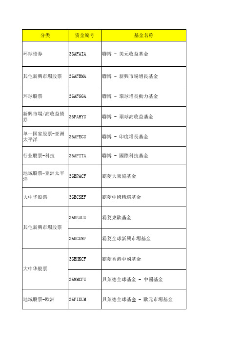
资金编号
基金名称
环球债券
36AFAIA
聯博 - 美元收益基金
其他新興市場股票
36AFRMA
聯博 - 新興市場增長基金
环球股票
36AFGGA
聯博 - 環球增長動力基金
新興市場/高收益债 36FAHYU 券 单一国家股票-亚洲 36AFEGU 太平洋 行业股票-科技 36AFITA
聯博 - 環球高收益基金
36SICOU
施羅德環球基金系列 - 中國優勢
地域股票-亚洲太平 36SCEAF 洋 新興市場/高收益债 36SCIMD 券
施羅德環球基金系列 - 新興亞洲
施羅德環球基金系列 - 新興市場債券
环球债券
36SIEBD
施羅德環球基金系列 - 歐元債券
行业股票-环境生态 36SGCCU
施羅德環球基金系列 - 環球氣候變化 策略
地域股票-亚洲太平 36HHADI 洋
亨德森遠見基金 - 亞洲股票收益基金
行业股票-房地产
36HHAPP
亨德森遠見基金 - 亞太地產股票基金
大中华股票
36HHCHI
亨德森遠見基金 - 中國躍升基金
行业股票-科技
36HHGTE
亨德森遠見基金 - 環球科技基金
日本股票
36HHJAP
亨德森遠見基金 - 日本股票基金
富達基金 - 歐洲增長基金
单一国家股票-亚洲 36FIIOD 太平洋 地域股票-亚洲太平 36FSEDA 洋 单一国家股票-亚洲 36FITHD 太平洋
富達基金 - 印尼基金
富達基金 - 東南亞基金
富達基金 - 泰國基金
环球债券
36FIUSB
富達基金 - 美元債券基金
HFBR-2412中文资料
Fiber-Optic Transmitter and ReceiverReliability Data IntroductionAgilent Technologies’ quality system includes an ongoing reliability monitor program to generate a data base from which this reliability data sheet is published.Transmitter Reliability The HFBR-0400 Series fiberoptic transmitters incorporate AlGaAs emitters and double lens optical systems. This design allows the HFBR-14XX transmitters to be driven at a relatively low current level for a specified amount of coupled power into the fiber. Because transmitter forward currents are proportional to failure rates, a low current translates into excellent transmitter reliability. To further improve reliability, Agilent has implemented a proprietary wafer screening technology that identifies dislocations whichcan lead to the formation of darkline defects (the primary mechanism for transmitter light output failures).HFBR-0400 SeriesTransmitters:HFBR-1402, -1412, -1404, -1414Receivers:HFBR-2402, -2412, -2406, -2416 Transmtter reliability data hasbeen calculated using 100 mAforward current and a 100% dutyfactor. In many actual useconditions, a 50% duty factor andlower forward currents are highlyprobable. When this is true,transmitter reliability will besubstantially better. The degree ofimprovement can be projected byexamining the footnotes below theHFBR-14XX data.Reliability PredictionModelThe reliability prediction modelused to project failure rate andmean time to failure (MTTF) atvarious temperatures shown in thesecond table assumes anexponential cumulative failurefunction (constant failure rate).The Arrhenius temperaturederating equation is used. AgilentTechnologies assumes no failuremechanism change between stressand use conditions. A conservativeactivation energy of 0.43 eV wasused and is derived from MIL-HDBD-217 for hybrid devices.Confidence intervals are basedupon the chi-squaredprediction method associated withexponential distributions.Fiber-Optic TransmitterReliability Data HFBR-1402HFBR-1412HFBR-1404HFBR-1414High Temperature Operating Life TestA. Demonstrated PerformanceTest Equivalent Test Condition Samples Device Hours Failures HTOL T A = 85°C, I F = 100 mA880 units879,5003B. Failure CriteriaFailure has occurred when the unitfails catastrophically, or when thelight output power decreases 3 dB.Point Typical PerformancePerformance [1]in Time [2]in Time(90% Confidence) Ambient Junction MTTF [1]FITs [3]MTTF [2]FITs [3] Temperature (°C)Temperature (°C)(hours)(/109 Hours)(hours)(/109 Hours) 85100293,0003411131,00075968095352,0002844158,00063347590424,0002360190,00052557085514,0001947231,00043376580626,0001598281,00035606075766,0001305344,00029055570945,0001059424,000235750651,172,000854526,000190145601,462,000684657,000152340551,838,000544825,000121235502,326,0004301,044,00095830452,965,0003371,331,00075125403,810,0002631,711,000585C. Failure Rate Prediction for Random Failures (I F @ 100 mA, 100% duty cycle)Notes:1. The point MTTF (representing an esti-mate of the mean point MTTF) is the total device hours divided by either the number performance that is expected from 90% ofall samples. This confidence interval isbased on the statistics of the distribution offailure rates prior to the onset of wear out.Refer to MIL-STD-690 for details of thismethodology.Fiber-Optic Link ReceiverReliability DataHFBR-2402HFBR-2412High Temperature Operating Life TestA. Demonstrated PerformanceTest Equivalent Test Condition Samples Device Hours Failures HTOL T A = 85°C, V CC = 5.25 V3,9602,370,0001B. Failure CriteriaFailure has occurred when the unitfails catastrophically. One devicefailed to switch logic states.Point Typical PerformancePerformance [1]in Time [2]in Time(90% Confidence) Ambient Junction MTTF [1]FITs [3]MTTF [2]FITs [3] Temperature (°C)Temperature (°C)(hours)(/109 Hours)(hours)(/109 Hours) 851002,370,000421609,0001,64080952,880,000346742,0001,34075903,530,000282909,0001,09070854,350,0002291,120,00089265805,400,0001841,390,00071960756,740,0001481,730,00057655708,480,0001172,180,000458506510,700,000932,750,000362456013,600,000733,510,000284405517,500,000564,520,000221355022,700,000435,850,000170304529,700,000337,650,000130254039,200,0002510,000,00099C. Failure Rate Prediction, Receiver (V CC = 5.25 V)Notes:1. The point MTTF (representing an esti-mate of the mean point MTTF) is the total device hours divided by either the number performance that is expected from 90% ofall samples. This confidence interval isuseful life failures. Refer to MIL-STD-690 fordetails of this methodology.Fiber-Optic Link ReceiverReliability DataHFBR-2406HFBR-2416High Temperature Operating Life TestA. Demonstrated PerformanceTest Equivalent Test Condition Samples Device Hours Failures HTOL T A = 85°C, V CC = 5.25 V2,2502,250,0000B. Failure CriteriaFailure has occurred when the unitfails catastrophically.Point Typical PerformancePerformance [1]in Time [2]in Time(90% Confidence) Ambient Junction MTTF [1]FITs [3]MTTF [2]FITs [3] Temperature (°C)Temperature (°C)(hours)(/109 Hours)(hours)(/109 Hours) 851002,250,000444977,164102380952,698,5163711,171,95385375903,252,6873071,412,62770870853,941,1732541,711,63358465804,801,4322082,085,24048060755,882,7441702,554,84939155707,250,3821383,148,80831850658,991,4071113,904,927256456011,222,799894,874,010205405514,102,949716,124,846163355017,848,023567,751,315129304522,755,516449,882,616101254029,238,4093412,698,10779C. Failure Rate Prediction, Receiver (V CC = 5.25 V)Notes:1. The point MTTF (representing an esti-mate of the mean point MTTF) is the total device hours divided by either the number performance that is expected from 90% ofall samples. This confidence interval isuseful life failures. Refer to MIL-STD-690 fordetails of this methodology.HFBR-0400 Mechanical and Environmental Test Data [1]MIL-STD-883D Units Total Test Name Reference Test Conditions Tested Failed Temperature Cycle1010500 cycles from -55 to +125°C, 15 minutes20201at extremes, 5 minutes transfer. [1]HFBR-1414500 cycles from -55 to +125°C, 15 minutes20900at extremes, 5 minutes transfer.[1]HFBR-2416 85/85T A = 85°C, 85% relative humidity,21407No bias, duration = 1,000 hours. [1]HFBR-1414T A = 85°C, 85% relative humidity,22206V CC = 5 volts, Duration = 1,000 hours[1]HFBR-2416 High Temperature1008T A = 125°C800 Storage Condition B1000 hoursResistance to2015Three 1 minute immersions.200 Solvents Brush after solvent immersion.Chemical Resistance— 5 minutes in Acetone, Methanol, Freon TF200and Boiling WaterVibration Variable 2007,20 G min., 20 to 2000 Hz.200 Frequency Condition B4, 4 minute cycles each X, Y, and Z.Thermal Shock1011-55°C to +125°C, 15 cycles600Condition B 5 min. dwell / 10 sec. transferMechanical Shock2002, 5 blows each X1, X2, Y1, Y2, Z1, Z2600Condition B1500 G, 0.5 msec. pulse.Port Wear Test [2]T A = 25°C500 connectorings200Less than 1 dBm variationConnector Side T A = 25°C 1 kg side load100 Load [3]Less than 1 dBm variationPort Strength [4]T A = 25°C 6 kg-cm (5.21 inch-lbs), no port damage100 Seal-Dye Penetrant101445 psi, 10 hours200 (Zyglo)Condition D No Leakage into microelectronic cavitySolderability2003245°C300 ESD Method 3015Human body model @ 10,000 V50HFBR-1414Human body model @ 2,000 V50HFBR-2402Human body model @ 1000 V50HFBR-2416Notes: See following page.Notes:1. Devices were preconditioned with 10 second, 260°C solder dip and 20 cycles, -40°C to 85°C, temperature cycle.2. Coupled power measurements were maximized before and after stress in determining the 1 dBm variation for SMA HFBR-0400 products. HFBR-0400 ST products do not require this due to the improved coupling design.3. The Connector Side Load test was only applied to HFBR-0400 SMA products. The Connector Side Load testing required that the housing be held so to prevent the leads from yielding. The load was applied through a SMA connectored fiber optic cable, perpendicular to the port. The product family is designed to limit cable and ferrule damage due to cable loading. The support and active leads should yield before damage to the cable or connector occurs. If extreme mechanical abuse of the cable/ connector is anticipated please contact Agilent’s Application Department for suggestions about mechanical strain relief. Due to the spring loaded feature of the ST connector, HFBR-0400 ST products will experience 1 dBm coupled power variation at a side load of less than 1 kg.4. The Port Strength test was designed to gauge the concerns with hand tightening the connector to the fiber optic port. The limit is set to alevel beyond most reasonable hand fastening loading.5. Package tests are defined as stresses that indicate the environmental strength of the package. Units tested indicate the total number of devices taken from the product family. While not all part numbers have been subjected to each stress, worst case products have been included.。
KDD25-24D03中文资料

KDD25 – 12 S 01MODEL LISTMODEL NO.INPUT VOLTAGEOUTPUT WATTAGEOUTPUT VOLTAGEOUTPUT CURRENTEFF .(MIN.)CASESingle Output ModelsKDD25 – 12S01 9~18 VDC 25 WATTS + 5 VDC 5000 mA 77% B KDD25 – 12S02 9~18 VDC 25 WATTS + 12 VDC 2100 mA 80% B KDD25 – 12S03 9~18 VDC 25 WATTS + 15 VDC 1700 mA 80% B KDD25 – 12S05 9~18 VDC 21.5 WATTS +3.3 VDC 6500 mA 75% B KDD25 – 24S01 18~36 VDC 25 WATTS + 5 VDC 5000 mA 79% B KDD25 – 24S02 18~36 VDC 25 WATTS + 12 VDC 2100 mA 81% B KDD25 – 24S03 18~36 VDC 25 WATTS + 15 VDC 1700 mA 81% B KDD25 – 24S05 18~36 VDC 21.5 WATTS +3.3 VDC 6500 mA 77% B KDD25 – 48S01 36~72 VDC 25 WATTS + 5 VDC 5000 mA 80% B KDD25 – 48S02 36~72 VDC 25 WATTS + 12 VDC 2100 mA 83% B KDD25 – 48S03 36~72 VDC 25 WATTS + 15 VDC 1700 mA 83% B KDD25 – 48S05 36~72 VDC 21.5 WATTS +3.3 VDC 6500 mA78% B Dual Output ModelsKDD25 – 12D01 9~18 VDC 25 WATTS ± 5 VDC +4700/-300 mA 77% B KDD25 – 12D02 9~18 VDC 25 WATTS ± 12 VDC +1800/-300 mA 80% B KDD25 – 12D03 9~18 VDC 25 WATTS ± 15 VDC +1400/-300 mA 80% B KDD25 – 24D01 18~36 VDC 25 WATTS ± 5 VDC +4700/-300 mA 79% B KDD25 – 24D02 18~36 VDC 25 WATTS ± 12 VDC +1800/-300 mA 81% B KDD25 – 24D03 18~36 VDC 25 WATTS ± 15 VDC +1400/-300 mA 81% B KDD25 – 48D01 36~72 VDC 25 WATTS ± 5 VDC +4700/-300 mA 80% B KDD25 – 48D02 36~72 VDC 25 WATTS ± 12 VDC +1800/-300 mA 83% B KDD25 – 48D0336~72 VDC25 WATTS± 15 VDC+1400/-300 mA83%BFEATURES* 2:1 INPUT RANGE* ISOLATION INPUT AND OUTPUT 1.5KV DC * HIGH PERFORMANCE UP TO 84% * SHORT CIRCUIT PROTECTION * 2 YEARS WARRANTY12 : 9~18V IN 24 : 18~36V IN 48:36~72V IN S : SINGLE OUTPUTD : DUAL OUTPUTWATTAGE 1: 5V OUT2: 12V OUT 3: 15V OUT 5: 3.3V OUTSPECIFICATIONAll Specifications Typical At Nominal Line, Full Load, 25 Unless Otherwise Noticed ℃GENERAL SPECIFICATION* Switching frequency: ......................... * Isolation voltage: .............................. * Isolation resistance: .......................... * Operating ambient temperature: ......... * Storage temperature: ........................ * Max. Case temperature: ..................... * M.T .B.F .: .......................................... * Cooling: ........................................... * Temperature coefficient: .................... * Dimension: ......................................80KHz 1,500VDC 1G Ω(min.) -25 to +71℃ -40 to +85℃ 90℃389,000Hrs at @ GF40, according to MIL-HDBK-217F Free air convection ±0.02% / ℃ 70 x 70 x 23mm INPUT SPECIFICATIONS* Input voltage range / frequency: .......... * Input filter: ....................................... * No load input current: ........................ * Max. Input voltage: ........................... 9 ~ 18VDC for 12V 18 ~ 36VDC for 24V 36 ~ 72VDC for 48V Pi type35mA for 12V in 30mA for 24V in 25mA for 12V in 20VDC for 12V in 40VDC for 24V in 75VDC for 48V inOUTPUT SPECIFICATIONS* Output voltage accuracy: ................... * Minimum load: .................................. * Line regulation: ................................ * Load regulation: ............................... * Ripple & noise: ................................. * Efficiency: ........................................ * Derating: ......................................... * Case material: ..................................±1 at Vo_nomNo load for single output models ±20% at Vo_nom for dual output models ±1% at Vo_nom±2% at Vo_nom for single output models ±5% at Vo_nom for dual output models Vout.x ±2%Up to 83%, see model list See table 1 Metal CONTROL AND PROTECTION* Input reversed: ................................. * Output short circuit: ..........................Shunt diode use external fuse Continuous[TABLE 1]90-25Ambient Temperture [℃]70600100P o w e r o u t [%]。
- 1、下载文档前请自行甄别文档内容的完整性,平台不提供额外的编辑、内容补充、找答案等附加服务。
- 2、"仅部分预览"的文档,不可在线预览部分如存在完整性等问题,可反馈申请退款(可完整预览的文档不适用该条件!)。
- 3、如文档侵犯您的权益,请联系客服反馈,我们会尽快为您处理(人工客服工作时间:9:00-18:30)。
Raltron Electronics Corporation 10651 NW 19th St. Miami, Florida 33172 U.S.A.
Tel: 305-593-6033 Fax: 305-594-3973 e-mail: sales@raltron.com Internet: http://www.raltron.com
SERIES H13K
SURFACE MOUNT MICROPROCESSOR CRYSTAL
FREQUENCY RANGE14.00 MHz TO 90.00 MHz
MODE OF OSCILLATION
(14.00 TO 40.320 MHz) FUNDAMENTAL
(40.00 TO 90.00 MHz) THIRD OVERTONE
FREQUENCY TOLERANCE AT 25°C±50 PPM MAXIMUM (±10 PPM, ±30 PPM AVAILABLE)
FREQUENCY STABILITY OVER
TEMPERATURE
±50 PPM MAXIMUM (±10 PPM, ±30 PPM AVAILABLE)
OPERATING TEMPERATURE RANGE
-10°C TO +60°C STANDARD
-30°C TO +85°C EXTENDED
STORAGE TEMPERATURE RANGE-30°C TO +85°C
AGING±5 PPM PER YEAR MAX.
LOAD CAPACITANCE12 pF TO 32 pF OR SERIES
EQUIVALENT SERIES RESISTANCE (ESR)SEE TABLE
SHUNT CAPACITANCE7.0 pF MAXIMUM
DRIVE LEVEL1 µW TO 100 µW
REFLOW CONDITIONS240° C FOR 10 s MAX 2 REFLOWS MAX
HOLDER TYPE-FREQUENCY-LOAD CAPACITANCE-MODE-EXTENDED TEMPERATURE-TAPE AND REEL
H13K IN MHz16 TO 32 pF FOR PARALLELS FOR SERIESFUND3OTFUNDAMENTALTHIRD OVERTONEEXTT
EXAMPLE: H13K-24.576-18-T
FEATURES
SPECIFICATIONS
PART NUMBERING SYSTEM
FREQUENCY(FUND)ESR (OHM)MAXFREQUENCY(FUND)ESR (OHM))MAXFREQUENCY3RD O/TESR (OHM)
MAX
14.318184524.003540.0065
14.74564524.5763540.32065
15.004527.003544.236865
15.3604528.003552.41665
16.003528.636363556.44865
16.93443529.49123566.66780
18.4323532.003570.0080
19.66083536.003580.0080
20.003540.003590.0080
23.0403540.32035
43
21
MARKING
AREA
.283 MAX
7.2 MAX
.
2
0
5
M
A
X
5
.
2
M
A
X
.051 MAX
1.3 MAX
.
0
3
9
1
.
0
.177
4.5
2
.
5
4
.012 R
0.3 R
.
1
0
0
.087
2.2.1574.0.0872.2
.056
1.4
.
0
5
6
1
.
4
.
0
4
3
1
.
1
PIN 1 LOCATION
PREHEATING
REFLOW
COOLING
240 °C
150 °C
25 °C
60
TIME (SECONDS)
T
E
M
P
E
R
A
T
U
R
E
200
1 TO 9 °C/s
1 TO 5 °C/s
10 s
1 TO 5 °C/s
1.55 ± .05 DIA
.06 ± .002 DIA
.16 ± .004
4 ± 0.1
1
.
7
5
±
0
.
1
.
0
6
9
±
.
0
0
4
1.8 ± 0.1
.071 ± .004
1
6
±
0
.
3
.
6
3
0
±
.
0
1
2
7
.
5
±
0
.
1
.
2
9
5
±
.
0
0
4
.315 ± .004
8.0 ± 0.1
7
.
5
±
0
.
1
2 ± 0.1
.079 ± .004
.
2
9
5
±
.
0
0
4
SOLDER REFLOW PROFILE
OUTLINE DRAWING
CARRIER TAPE DIMENSIONS
Scale none Dimension in
mm
inch
SOLDER PATTERN
255mm REEL DIAMETER
16mm TAPE WIDTH, 8mm PITCH
QUANTITY: 1000 PIECES PER REEL
PACKAGING
ALSO AVAILABLE IN ULTRA-THIN 1.0 mm HEIGHT
TIGHT TOLERANCE AND STABILITY TO ± 10 PPM
WIDE FREQUENCY RANGE
元器件交易网www.cecb2b.com