top242-250cn
TLV2543CN;TLV2543CDBR;TLV2543CDW;TLV2543IDB;TLV2543IDW;中文规格书,Datasheet资料

Terminal Functions
TERMINAL NAME AIN0 – AIN10 NO. 1 – 9, 11, 12 15 I/O I DESCRIPTION Analog input. These 11 analog-signal inputs are internally multiplexed. The driving source impedance should be less than or equal to 50 Ω for 4.1-MHz I/O CLOCK operation and capable of slewing the analog input voltage into a capacitance of 60 pF. Chip select. A high-to-low transition on CS resets the internal counters and controls and enables DATA OUT, DATA INPUT, and I/O CLOCK. A low-to-high transition disables DATA INPUT and I/O CLOCK within a setup time. Serial-data input. A 4-bit serial address selects the desired analog input or test voltage to be converted. The serial data is presented with the MSB first and is shifted in on the first four rising edges of I/O CLOCK. After the four address bits are read into the address register, I/O CLOCK clocks the remaining bits in order. Serial data output. This is the 3-state serial output for the A/D conversion result. DATA OUT is in the high-impedance state when CS is high and active when CS is low. With a valid CS, DATA OUT is removed from the high-impedance state and is driven to the logic level corresponding to the MSB/LSB value of the previous conversion result. The next falling edge of I/O CLOCK drives DATA OUT to the logic level corresponding to the next MSB / LSB, and the remaining bits are shifted out in order. End of conversion. EOC goes from a high to a low logic level after the falling edge of the last I/O CLOCK and remains low until the conversion is complete and data are ready for transfer. Ground. This is the ground return terminal for the internal circuitry. Unless otherwise noted, all voltage measurements are with respect to GND. I Input /output clock. I/O CLOCK receives the serial input and performs the following four functions: 1. It clocks the eight input data bits into the input data register on the first eight rising edges of I/O CLOCK with the multiplexer address available after the fourth rising edge. 2. On the fourth falling edge of I/O CLOCK, the analog input voltage on the selected multiplexer input begins charging the capacitor array and continues to do so until the last falling edge of I/O CLOCK. 3. It shifts the 11 remaining bits of the previous conversion data out on DATA OUT. Data changes on the falling edge of I/O CLOCK. 4. It transfers control of the conversion to the internal state controller on the falling edge of the last I/O CLOCK. Reference +. The upper reference voltage value (nominally VCC) is applied to REF+. The maximum input voltage range is determined by the difference between the voltage applied to this terminal and the voltage applied to the REF – terminal. Reference –. The lower reference voltage value (nominally ground) is applied to REF –. Positive supply voltage.
诺基亚 ONT G-2425G-A(外部天线) 技术规格书说明书
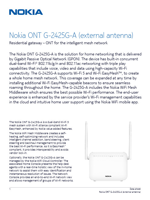
The Nokia ONT G-2425G-A is a dual-band Wi-Fi 5 mesh system with Wi-Fi Alliance compliant Wi-Fi EasyMesh, enhanced by Nokia value added features.The Nokia WiFi Mesh Middleware creates a self-healing, self-optimizing network and includes intelligent channel selection, band steering, client steering and backhaul management to provide the best Wi-Fi performance. As it is EasyMesh ™ compliant, it provides interoperability and avoids vendor lock-in.Optionally, the Nokia ONT G-2425G-A can be managed by the Nokia WiFi Cloud Controller. The associated Home Console presents the help desk agents with a real-time holistic view of the in-home network to assist them with easy identification and instantaneous resolution of issues. The Network Console provides an end-to-end Wi-Fi network view and allows management of groups of Wi-Fi networks.Nokia ONT G-2425G-A (external antenna)Residential gateway – ONT for the intelligent mesh networkThe Nokia ONT G-2425G-A is the solution for home networking that is delivered by Gigabit Passive Optical Network (GPON). The device has built-in concurrent dual-band Wi-Fi ® 802.11b/g/n and 802.11ac networking with triple play capabilities that include voice, video and data using high-capacity Wi-Ficonnectivity. The G-2425G-A supports Wi-Fi 5 and Wi-Fi EasyMesh™, to create a whole home mesh network. This coverage can be expanded at any time by installing additional Wi-Fi EasyMesh-capable beacons to ensure seamless roaming throughout the home. The G-2425G-A includes the Nokia WiFi Mesh Middleware which ensures the best possible Wi-Fi performance. The end-user experience is enhanced by the service provider’s Wi-Fi management capabilitiesin the cloud and intuitive home user support using the Nokia WiFi mobile app.This Nokia indoor ONT is designed to deliver triple play services (voice, video and data) to residential subscribers. Voice services are provided through two plain old telephone service (POTS) ports withan integrated analog telephone adapter (ATA)that converts voice traffic into Session Initiation Protocol (SIP). Connectivity to an existing public switched telephone network (PSTN) Class 5 switchis supported through SIP with direct interoperability of a variety of soft switches. Ethernet connectivity is available on four Gigabit Ethernet (GigE) ports, all of which have the ability to burst up to a full gigabit dynamically. Service providers can deliver video using IP packets (IPTV).Relying on dual-band Wi-Fi allows for support ofthe widest range of customer products. The IEEE 802.11ac standard enables gigabit speeds on many newer devices, while the widely supported 802.11b/g/n standard can simultaneously connect to legacy devices.Features• Four RJ-45 10/100/1000 Ethernet ports• Two POTS ports for carrier-grade voice services • Dual-band concurrent Wi-Fi: 2.4GHz and 5GHz • Wireless IEEE 802.11b/g/n: 2.4GHz• Wireless IEEE 802.11ac: 5GHz• Network Address Translation (NAT) and firewall • Voice interworking function from the analog POTS lines to the voice over IP (VoIP) and Ethernet layers • Two USB 2.0 host ports• Optics support received signal strength indication (RSSI)• Supports virtual private network (VPN) passthrough for Point-to-Point Tunneling Protocol (PPTP), Layer 2 Tunneling Protocol (L2TP) and IPSec• Port forwarding and demilitarized zone (DMZ)/ dynamic domain name system (DDNS)Benefits• EasyMesh enhanced by Nokia value added features • Integrates the ONT and wireless access pointfunctions to allow for one less device in the home • Delivers connectivity to Ethernet devices within the home• Supports full triple play services, including voice, video and data• Allows service-per-port configurations• Supports IP video distribution• Supports easy-to-use USB 2.0 connections for external disk drives and home network attached storage (NAS)• Delivers voice services using VoIP• Delivers video services efficiently with multicasting or unicasting• Facilitates network management using Nokia 5520 AMS• Flexible video delivery options of Ethernet or wireless to set-top boxes (STBs) Technical specifications Physical• Height: 131 mm (5.1 in)–Excluding antenna of 170 mm (6.7 in)• Width: 170 mm (6.7 in)• Depth: 30 mm (1.2 in)• Weight: 0.42 kg (0.92 lb)Installation• Desk mountable• Wall mountable with bracketOperating environment• Temperature: -5°C to 45°C (23°F to 113°F)• Relative humidity: 10% to 90%Power requirements• Local powering with 12 V input (feed uses external AC/DC adapter)• Dying gasp support• Power consumption: <24 WGPON uplinks• Wavelength: 1490 nm downstream, 1310 nm upstream• Line rate: 2.488 Gb/s downstream, 1.244 Gb/s upstream• GPON Encapsulation Method (GEM) mode support for IP/Ethernet service traffic• ITU-T G.984.3-compliant dynamic bandwidth reporting• ITU-T G.984.3-compliant Advanced Encryption Standard (AES) in downstream• ITU-T G.984.3-compliant forward error correction (FEC)• ITU-T G.988 Appendix 1 and Appendix 2 ONT Management Control Interface (OMCI)• Remote software image download• BOSA On Board (BOB) type laser, SC/APC connectorEthernet interfaces• 10/100/1000Base-T interface with RJ-45 connectors• Wi-Fi Protected Access (WPA) support, including pre-shared key (WPA-PSK) and WPA2• Forwarding• Ethernet port auto-negotiation or manual configuration with medium dependent interface/ medium dependent interface crossover(MDI/MDIX)• Virtual switch based on IEEE 802.1q virtual LAN (VLAN)• VLAN tagging/de-tagging per Ethernet port and marking/remarking of IEEE 802.1p • IP type of service/differentiated services code point (ToS/DSCP) to IEEE 802.1p mapping for untagged frames• Class of service (CoS) based on VLAN ID, IEEE 802.1p bit• Internet Group Management Protocol (IGMP)v2/v3 snoopingPOTS interfaces• Two FXS ports for VoIP service with RJ-11 connectors• Multiple codecs: ITU-T G.711, ITU-T G.729• SIP (RFC 3261)• ITU-T G.168 echo cancellation• Services: caller ID, call waiting, call hold, 3-way call, call transfer, message waiting indication• 3 ringer equivalence numbers (RENs) per line • Dual-tone multi-frequency (DTMF) dialing• Balanced sinusoidal ring signal, 55 V root mean square (RMS)WLAN interfaces• 2x2 MIMO on 802.11b/g/n• 2x2 MIMO on 802.11ac• 5 dBi external antenna• WPA, WPA-PSK/TKIP, WPA2, WPA2-PSK/AES• Media access control (MAC) filtersUSB interface• Two USB 2.0 interfacesResidential gateways• IPv4 and IPv6• Point-to-Point Protocol over Ethernet (PPPoE) and IP over Ethernet (IPoE)• NAT, DMZ and firewall• Dynamic Host Configuration Protocol (DHCP) and domain name system (DNS) proxy• IGMP proxy• Supports TR-069About NokiaWe create the technology to connect the world. Only Nokia offers a comprehensive portfolio of network equipment, software, services and licensing opportunities across the globe. With our commitment to innovation, driven by the award-winning Nokia Bell Labs, we are a leader in the development and deployment of 5G networks.Our communications service provider customers support more than 6.4 billion subscriptions with our radio networks, and our enterprise customers have deployed over 1,300 industrial networks worldwide. Adhering to the highest ethical standards, we transform how people live, work and communicate. For our latest updates, please visit us online and follow us on Twitter @nokia.Nokia operates a policy of ongoing development and has made all reasonable efforts to ensure that the content of this document is adequate and free of material errors and omissions. Nokia assumes no responsibility for any inaccuracies in this document and reserves the right to change, modify, transfer, or otherwise revise this publication without notice.Nokia is a registered trademark of Nokia Corporation. Other product and company names mentioned herein may be trademarks or trade names of their respective owners.© 2020 NokiaNokia Oyj Karaportti 3FI-02610 Espoo, Finland LEDs• Power • Link • Auth • LAN (1~4)• TEL (1~2)• VoIP• Wi-Fi Protected Setup (WPS) 2.4GHz/5GHz • WLAN 2.4GHz/5GHz • USB • InternetSafety and electromagnetic interference (EMI)• Protection of over voltage/currentRegulatory compliances• CE Mark • FCC Mark。
top249yn

TOP242 P or G 9 W TOP242 R 15 W TOP242 Y or F 10 W TOP243 P or G 13 W TOP243 R 29 W TOP243 Y or F 20 W TOP244 P or G 16 W TOP244 R 34 W TOP244 Y or F 30 W TOP245 P or G 19 W TOP245 R 37 W TOP245 Y or F 40 W TOP246 P or G 21 W TOP246 R 40 W TOP246 Y or F 60 W 42 W TOP247 R TOP247 Y or F 85 W 43 W TOP248 R TOP248 Y or F 105 W 44 W TOP249 R TOP249 Y or F 120 W 45 W TOP250 R TOP250 Y or F 135 W
Extended Power, Design Flexible, ® EcoSmart, Integrated Off-line Switcher
AC IN
+ DBiblioteka OUT -DLCONTROL
TOPSwitch-GX
S
C
X
F
PI-2632-060200
Figure 1. Typical Flyback Application.
Table 1. Notes: 1. Typical continuous power in a non-ventilated enclosed adapter measured at 50 °C ambient. 2. Maximum practical continuous power in an open frame design at 50 °C ambient. See Key Applications for detailed conditions. 3. For lead-free package options, see Part Ordering Information. 4. 230 VAC or 100/115 VAC with doubler.
超通TC6215高电压低阈值双通道MOSFET说明书
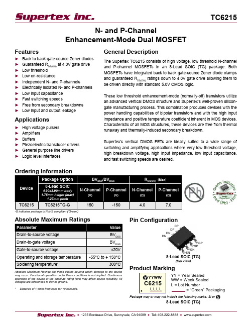
FeaturesBack to back gate-source Zener diodes Guaranteed R DS(ON) at 4.0V gate drive Low threshold Low on-resistanceIndependent N- and P-channelsElectrically isolated N- and P-channels Low input capacitance Fast switching speedsFree from secondary breakdowns Low input and output leakageApplicationsHigh voltage pulsers Amplifiers BuffersPiezoelectric transducer drivers General purpose line drivers Logic level interfaces►►►►►►►►►►►►►►►►General DescriptionThe Supertex TC6215 consists of high voltage, low threshold N-channel and P-channel MOSFETs in an 8-Lead SOIC (TG) package. Both MOSFETs have integrated back to back gate-source Zener diode clamps and guaranteed R DS(ON) ratings down to 4.0V gate drive allowing them to be driven directly with standard 5.0V CMOS logic.These low threshold enhancement-mode (normally-off) transistors utilize an advanced vertical DMOS structure and Supertex’s well-proven silicon-gate manufacturing process. This combination produces devices with the power handling capabilities of bipolar transistors and with the high input impedance and positive temperature coefficient inherent in MOS devices. Characteristic of all MOS structures, these devices are free from thermal runaway and thermally-induced secondary breakdown.Supertex’s vertical DMOS FETs are ideally suitedto a wide range of switching and amplifying applications where very low threshold voltage, high breakdown voltage, high input impedance, low input capacitance, and fast switching speeds are desired.N- and P-ChannelEnhancement-Mode Dual MOSFET-G indicates package is RoHS compliant (‘Green’)GP SP GN SNDP DP DN DNYY = Year Sealed WW = Week Sealed L = Lot Number= “Green” Packaging 8-Lead SOIC (TG)(top view)Absolute Maximum Ratings are those values beyond which damage to the device may occur. Functional operation under these conditions is not implied. Continuous operation of the device at the absolute rating level may affect device reliability. All voltages are referenced to device ground.* Distance of 1.6mm from case for 10 seconds.8-Lead SOIC (TG)Package may or may not include the following marks: Si orPin ConfigurationN-Channel Switching Waveforms and Test CircuitVOUTPUT 10V0V0VVDDInputOutputNotes:All DC parameters 100% tested at 25°C unless otherwise stated. (Pulsed test: 300µs pulse at 2% duty cycle.)All AC parameters sample tested.1.2.DD0V -10V0V V DDInputOutputNotes:All DC parameters 100% tested at 25°C unless otherwise stated. (Pulsed test: 300µs pulse at 2% duty cycle.)All AC parameters sample tested.1.2.Block DiagramSN GN SPGPDPDPDN DN 8-Lead SOIC(top view)P-Channel Output Characteristics-4.0-3.5-3.0-2.5-2.0-1.5-1.0-0.50.0-50-45-40-35-30-25-20-15-10-5V DS (volts)I D (a m p e r e s )V =-10VV =-8V V =-7VV =-6VV =-5VV =-4VV =-3VV =-2VP-Channel Saturation Characteristics-2.2-2.0-1.8-1.6-1.4-1.2-1.0-0.8-0.6-0.4-0.20.0-10-9-8-7-6-5-4-3-2-1V DS (volts)I D (a m p e r e s )V GS =-10V V GS =-8V V GS =-6V V GS =-5VV GS =-4VV GS =-3VV GS =-2VN-Channel Output Characteristics0.00.51.01.52.02.53.03.54.04.505101520253035404550V DS (volts)I D (a m p e r e s )V GS =10V V GS =8V V GS =7VV GS =6VV GS =5VV GS =4VV GS =3VV GS =2VN-Channel Saturation Characteristics0.00.51.01.52.02.53.03.54.012345678910V DS (volts)I D (a m p e r e s )V GS =10V V GS =8V V GS =6VV GS =5VV GS =4VV GS =3VV GS =2VTypical Performance CurvesSupertex inc. does not recommend the use of its products in life support applications, and will not knowingly sell them for use in such applications unless it receives an adequate “product liability indemnification insurance agreement.” Supertex inc. does not assume responsibility for use of devices described, and limits its liability to the replacement of the devices determined defective due to workmanship. No responsibility is assumed for possible omissions and inaccuracies. Circuitry and specifications are subject to change without notice. For the latest product specifications refer to the Supertex inc. website: http//.©2008 All rights reserved. Unauthorized use or reproduction is prohibited.1235 Bordeaux Drive, Sunnyvale, CA 94089(The package drawing(s) in this data sheet may not reflect the most current specifications. For the latest package outline information go to /packaging.html .)8-Lead SOIC (Narrow Body) Package Outline (TG)4.90x3.90mm body, 1.75mm height (max), 1.27mm pitchSide ViewView A-AJEDEC Registration MS-012, Variation AA, Issue E, Sept. 2005.* This dimension is not specified in the original JEDEC drawing. The value listed is for reference only.Drawings are not to scale.Supertex Doc. #: DSPD-8SOLGTG, Version H101708.Note:This chamfer feature is optional. A Pin 1 identifier must be located in the index area indicated. The Pin 1 identifier can be: a molded mark/identifier;an embedded metal marker; or a printed indicator.1.。
TOP244Y中文资料

®
+ DC OUT -
D
L
CONTROL
TOPSwitch-GX
S X F
C
PI-2632-060200
ቤተ መጻሕፍቲ ባይዱ
Figure 1. Typical Flyback Application.
OUTPUT POWER TABLE
230 VAC ±15%4 85-265 VAC Adapter1 Open Frame2
6.5 W 7W 7W 9W 15 W 15 W 11 W 18 W 20 W 20 W 26 W 24 W 40 W 26 W 55 W 28 W 70 W 30 W 80 W
10 W 14 W 14 W 15 W 23 W 30 W 20 W 28 W 45 W 32 W 60 W 36 W 90 W 43 W 125 W 48 W 155 W 52 W 180 W
Table 1. Notes: 1. Typical continuous power in a non-ventilated enclosed adapter measured at 50 °C ambient. Assumes 1 sq. in. of 2 oz. copper heat sink area for R package. 2. Maximum practical continuous power in an open frame design at 50 °C ambient. See Key Applications for detailed conditions. Assumes 3 sq. in. of 2 oz. copper heat sink area for R package. 3. See Part Ordering Information. 4. 230 VAC or 100/115 VAC with doubler.
top258pn

TOP252-262TOPSwitch-HX Family January 2009Enhanced EcoSmart ®, Integrated Off-Line Switcher with Advanced Feature Set and Extended Power Range®Product HighlightsLower System Cost, Higher Design FlexibilityMulti-mode operation maximizes efficiency at all loads New eSIP-7F and eSIP-7C packagesLow thermal impedance junction-to-case (2 °C per watt)Low height is ideal for adapters where space is limitedSimple mounting using a clip to aid low cost manufacturing Horizontal eSIP-7F package ideal for ultra low height adapter and monitor applicationsExtended package creepage distance from DRAIN pin to adjacent pin and to heat sinkNo heatsink required up to 35 W using P , G and M packages with universal input voltage and up to 48 W at 230 VACOutput overvoltage protection (OVP) is user programmable for latching/non-latching shutdown with fast AC reset Allows both primary and secondary sensingLine undervoltage (UV) detection prevents turn-off glitches Line overvoltage (OV) shutdown extends line surge limit Accurate programmable current limitOptimized line feed-forward for line ripple rejection132 kHz frequency (254Y-258Y and all E/L packages) reduces transformer and power supply sizeHalf frequency option for video applications Frequency jittering reduces EMI fi lter cost •••••••••••••••••Figure 1. Typical Flyback Application.Heatsink is connected to SOURCE for low EMIImproved auto-restart delivers <3% of maximum power in short circuit and open loop fault conditionsAccurate hysteretic thermal shutdown function automatically recovers without requiring a resetFully integrated soft-start for minimum start-up stress Extended creepage between DRAIN and all other pins improves fi eld reliability•••••Table 1.Output Power Table. (for notes see page 2).Rev. F 01/09EcoSmart ®– Energy Effi cientEnergy efficient over entire load range No-load consumptionLess than 200 mW at 230 VAC Standby power for 1 W input>600 mW output at 110 VAC input >500 mW output at 265 VAC inputDescriptionTOPSwitch-HX cost effectively incorporates a 700 V power MOSFET, high voltage switched current source, PWM control, oscillator, thermal shutdown circuit, fault protection and other control circuitry onto a monolithic device.••••••Figure 2. Typical Flyback Application TOP259YN, TOP260YN and TOP261YN.Y Package Option for TOP259-261In order to improve noise-immunity on large TOPSwitch-HX Y package parts, the F pin has been removed (TOP259-261YN are fi xed at 66 kHz switching frequency) and replaced with a SIGNAL GROUND (G) pin. This pin acts as a low noise path for the C pin capacitor and the X pin resistor. It is only required for the TOP259-261YN package parts.Notes for Table 1:1. Minimum continuous power in a typical non-ventilatedenclosed adapter measured at +50 °C ambient. Use of an external heat sink will increase power capability. 2. Minimum continuous power in an open frame design at+50 °C ambient.3. Peak power capability in any design at +50 °C ambient.4. 230 VAC or 110/115 VAC with doubler.5. Packages: P: DIP-8C, G: SMD-8C, M: SDIP-10C,Y: TO-220-7C, E: eSIP-7C, L: eSIP-7F .See part ordering information.6. TOP261 and TOP262 have the same current limit set point. Insome applications TOP262 may run cooler than TOP261 due to a lower R DS(ON) for the larger device.7. TOP256E package parts are available with Green (HalogenFree) mold compound. See Part Ordering Information on page 47. Parametrically green material encapsulated E package parts are identical to non-green parts. Section ListFunctional Block Diagram (4)Pin Functional Description (6)TOPSwitch-HX Family Functional Description (7)CONTROL (C) Pin Operation (8)Oscillator and Switching Frequency (8)Pulse Width Modulator (9)Maximum Load Cycle (9)ErrorAmplifier (9)On-Chip Current Limit with External Programmability (9)Line Under-Voltage Detection (UV) (10)Line Overvoltage Shutdown (OV) (11)Hysteretic or Latching Output Overvoltage Protection (OVP) (11)Line Feed-Forward with DCMAX Reduction (13)Remote ON/OFF and Synchronization (13)Soft-Start (13)Shutdown/Auto-Restart (13)Hysteretic Over-Temperature Protection (13)BandgapReference (13)High-Voltage Bias Current Source (13)Typical Uses of FREQUENCY (F) Pin (15)Typical Uses of VOLTAGE MONITOR (V) and EXTERNAL CURRENT LIMIT (X) Pins (16)Typical Uses of MULTI-FUNCTION (M) Pin (18)Application Examples (21)A High Effi ciency, 35 W, Dual Output – Universal Input Power Supply (21)A High Effi ciency, 1500 W, 250-380 VDC Input Power Supply (22)A High Effi ciency, 20 W Continuous – 80 W Peak, Universal Input Power Supply (23)A High Effi ciency, 65 W, Universal Input Power Supply (24)Key Application Considerations (25)TOPSwitch-HX vs.TOPSwitch-GX (25)TOPSwitch-HX Design Considerations (26)TOPSwitch-HX Layout Considerations (27)Quick Design Checklist (31)DesignTools (31)Product Specifi cations and Test Conditions (32)Typical Performance Characteristics (39)Package Outlines (43)Part Ordering Information (47)Rev. F 01/09Rev. F 01/09Figure 3a. Functional Block Diagram (P and G Packages).Figure 3b. Functional Block Diagram (M Package).Rev. F 01/09Figure 3c. Functional Block Diagram (TOP254-258 YN Package and all eSIP Packages).Figure 3d. Functional Block Diagram TOP259YN, TOP260YN, TOP261YN.Rev. F 01/09Pin Functional DescriptionDRAIN (D) Pin:High-voltage power MOSFET DRAIN pin. The internal start-up bias current is drawn from this pin through a switched high-voltage current source. Internal current limit sense point for drain current.CONTROL (C) Pin:Error amplifi er and feedback current input pin for duty cycle control. Internal shunt regulator connection to provide internal bias current during normal operation. It is also used as the connection point for the supply bypass and auto-restart/compensation capacitor.EXTERNAL CURRENT LIMIT (X) Pin (Y, M, E and L package):Input pin for external current limit adjustment and remote ON/OFF. A connection to SOURCE pin disables all functions on this pin.Figure 4. Pin Confi guration (Top View).P I -4711-021308Figure 5. TOP254-258 Y and All M/E/L Package Line Sense and Externally Set Current Limit.Figure 7. P/G Package Line Sense.P I -4983-021308Figure 6. TOP259-261 Y Package Line Sense and External Current Limit.VOLTAGE MONITOR (V) Pin (Y & M package only):Input for OV, UV, line feed forward with DC MAX reduction, output overvoltage protection (OVP), remote ON/OFF and device reset. A connection to the SOURCE pin disables all functions on this pin.MULTI-FUNCTION (M) Pin (P & G packages only):This pin combines the functions of the VOLTAGE MONITOR (V) and EXTERNAL CURRENT LIMIT (X) pins of the Y package into one pin. Input pin for OV, UV, line feed forward with DC MAXRev. F 01/09Figure 8. P/G Package Externally Set Current Limit.reduction, output overvoltage protection (OVP), external current limit adjustment, remote ON/OFF and device reset. Aconnection to SOURCE pin disables all functions on this pin and makes TOPSwitch-HX operate in simple three terminal mode (like TOPSwitch-II).FREQUENCY (F) Pin (TOP254-258Y, and all E and L packages):Input pin for selecting switching frequency 132 kHz if connected to SOURCE pin and 66 kHz if connected to CONTROL pin. The switching frequency is internally set for fi xed 66 kHzoperation in the P , G, M package and TOP259YN, TOP260YN and TOP261YN.SIGNAL GROUND (G) Pin (TOP259YN, TOP260YN & TOP261YN only):Return for C pin capacitor and X pin resistor.SOURCE (S) Pin:Output MOSFET source connection for high voltage power return. Primary side control circuit common and reference point.TOPSwitch-HX Family Functional DescriptionLike TOPSwitch-GX, TOPSwitch-HX is an integrated switched mode power supply chip that converts a current at the control input to a duty cycle at the open drain output of a high voltage power MOSFET. During normal operation the duty cycle of the power MOSFET decreases linearly with increasing CONTROL pin current as shown in Figure 9.In addition to the three terminal TOPSwitch features, such as the high voltage start-up, the cycle-by-cycle current limiting, loop compensation circuitry, auto-restart and thermalshutdown, the TOPSwitch-HX incorporates many additional functions that reduce system cost, increase power supply performance and design fl exibility. A patented high voltageCMOS technology allows both the high-voltage power MOSFET and all the low voltage control circuitry to be cost effectively integrated onto a single monolithic chip.Three terminals, FREQUENCY, VOLTAGE-MONITOR, andEXTERNAL CURRENT LIMIT (available in Y and E/L packages),two terminals, VOLTAGE-MONITOR and EXTERNAL CURRENT LIMIT (available in M package) or one terminal MULTI-FUNCTION (available in P and G package) have been used to implement some of the new functions. These terminals can be connected to the SOURCE pin to operate the TOPSwitch-HX in aTOPSwitch-like three terminal mode. However, even in this three terminal mode, the TOPSwitch-HX offers many transparent features that do not require any external components:A fully integrated 17 ms soft-start significantly reduces or eliminates output overshoot in most applications by sweeping both current limit and frequency from low to high to limit the peak currents and voltages during start-up.A maximum duty cycle (DC MAX ) of 78% allows smaller inputstorage capacitor, lower input voltage requirement and/or higher power capability.Multi-mode operation optimizes and improves the powersupply effi ciency over the entire load range while maintaining good cross regulation in multi-output supplies.1.2.3.Figure 9. Control Pin Characteristics (Multi-Mode Operation).Rev. F 01/09Switching frequency of 132 kHz reduces the transformer sizewith no noticeable impact on EMI.Frequency jittering reduces EMI in the full frequency mode athigh load condition.Hysteretic over-temperature shutdown ensures automaticrecovery from thermal fault. Large hysteresis prevents circuit board overheating.Packages with omitted pins and lead forming provide largedrain creepage distance.Reduction of the auto-restart duty cycle and frequency toimprove the protection of the power supply and load during open loop fault, short circuit, or loss of regulation.Tighter tolerances on I 2f power coeffi cient, current limitreduction, PWM gain and thermal shutdown threshold.The VOLTAGE-MONITOR (V) pin is usually used for line sensing by connecting a 4 M Ω resistor from this pin to the rectifi ed DC high voltage bus to implement line overvoltage (OV), under-voltage (UV) and dual-slope line feed-forward with DC MAXreduction. In this mode, the value of the resistor determines the OV/UV thresholds and the DC MAX is reduced linearly with a dual slope to improve line ripple rejection. In addition, it also provides another threshold to implement the latched and hysteretic output overvoltage protection (OVP). The pin can also be used as a remote ON/OFF using the I UV threshold.The EXTERNAL CURRENT LIMIT (X) pin can be used to reduce the current limit externally to a value close to the operating peak current, by connecting the pin to SOURCE through a resistor. This pin can also be used as a remote ON/OFF input.For the P and G package the VOLTAGE-MONITOR andEXTERNAL CURRENT LIMIT pin functions are combined on one MULTI-FUNCTION (M) pin. However, some of the functions become mutually exclusive.The FREQUENCY (F) pin in the TOP254-258 Y and E/L packages set the switching frequency in the full frequency PWM mode to the default value of 132 kHz when connected to SOURCE pin. A half frequency option of 66 kHz can be chosen by connecting this pin to the CONTROL pin instead. Leaving this pin open is not recommended. In the P , G and M packages and the TOP259-261 Y packages, the frequency is set internally at 66 kHz in the full frequency PWM mode.CONTROL (C) Pin OperationThe CONTROL pin is a low impedance node that is capable of receiving a combined supply and feedback current. During normal operation, a shunt regulator is used to separate thefeedback signal from the supply current. CONTROL pin voltage V C is the supply voltage for the control circuitry including the MOSFET gate driver. An external bypass capacitor closely connected between the CONTROL and SOURCE pins is required to supply the instantaneous gate drive current. The total amount of capacitance connected to this pin also sets the auto-restart timing as well as control loop compensation.When rectifi ed DC high voltage is applied to the DRAIN pin during start-up, the MOSFET is initially off, and the CONTROL pin capacitor is charged through a switched high voltage4.5.6.7.8.9.current source connected internally between the DRAIN and CONTROL pins. When the CONTROL pin voltage V C reaches approximately 5.8 V, the control circuitry is activated and the soft-start begins. The soft-start circuit gradually increases the drain peak current and switching frequency from a low starting value to the maximum drain peak current at the full frequency over approximately 17 ms. If no external feedback/supplycurrent is fed into the CONTROL pin by the end of the soft-start, the high voltage current source is turned off and the CONTROL pin will start discharging in response to the supply current drawn by the control circuitry. If the power supply is designed properly, and no fault condition such as open loop or shorted output exists, the feedback loop will close, providing external CONTROL pin current, before the CONTROL pin voltage has had a chance to discharge to the lower threshold voltage of approximately 4.8 V (internal supply undervoltage lockout threshold). When the externally fed current charges theCONTROL pin to the shunt regulator voltage of 5.8 V, current in excess of the consumption of the chip is shunted to SOURCE through an NMOS current mirror as shown in Figure 3. The output current of that NMOS current mirror controls the duty cycle of the power MOSFET to provide closed loop regulation. The shunt regulator has a fi nite low output impedance Z C that sets the gain of the error amplifi er when used in a primary feedback confi guration. The dynamic impedance Z C of the CONTROL pin together with the external CONTROL pin capacitance sets the dominant pole for the control loop.When a fault condition such as an open loop or shorted output prevents the fl ow of an external current into the CONTROL pin, the capacitor on the CONTROL pin discharges towards 4.8 V. At 4.8 V, auto-restart is activated, which turns the output MOSFET off and puts the control circuitry in a low current standby mode. The high-voltage current source turns on and charges the external capacitance again. A hysteretic internal supply undervoltage comparator keeps V C within a window of typically 4.8 V to 5.8 V by turning the high-voltage current source on and off as shown in Figure 11. The auto-restart circuit has a divide-by-sixteen counter, which prevents the output MOSFET from turning on again until sixteen discharge/charge cycles have elapsed. This is accomplished by enabling the output MOSFET only when the divide-by-sixteen counter reaches the full count (S15). The counter effectively limitsTOPSwitch-HX power dissipation by reducing the auto-restart duty cycle to typically 2%. Auto-restart mode continues until output voltage regulation is again achieved through closure of the feedback loop.Oscillator and Switching FrequencyThe internal oscillator linearly charges and discharges an internal capacitance between two voltage levels to create atriangular waveform for the timing of the pulse width modulator. This oscillator sets the pulse width modulator/current limit latch at the beginning of each cycle.The nominal full switching frequency of 132 kHz was chosen to minimize transformer size while keeping the fundamental EMI frequency below 150 kHz. The FREQUENCY pin (available only in TOP254-258 Y and E, L packages), when shorted to the CONTROL pin, lowers the full switching frequency to 66 kHzRev. F 01/09Figure 10. Switching Frequency Jitter (Idealized V DRAIN Waveforms).(half frequency), which may be preferable in some cases such as noise sensitive video applications or a high effi ciency standby mode. Otherwise, the FREQUENCY pin should be connected to the SOURCE pin for the default 132 kHz. In the M, P and G packages and the TOP259-261 Y package option, the full frequency PWM mode is set at 66 kHz, for higher effi ciency and increased output power in all applications.To further reduce the EMI level, the switching frequency in the full frequency PWM mode is jittered (frequency modulated) by approximately ±2.5 kHz for 66 kHz operation or ±5 kHz for 132 kHz operation at a 250 Hz (typical) rate as shown in Figure 10. The jitter is turned off gradually as the system is entering the variable frequency mode with a fi xed peak drain current.Pulse Width ModulatorThe pulse width modulator implements multi-mode control by driving the output MOSFET with a duty cycle inversely proportional to the current into the CONTROL pin that is in excess of the internal supply current of the chip (see Figure 9). The feedback error signal, in the form of the excess current, is fi ltered by an RC network with a typical corner frequency of 7 kHz to reduce the effect of switching noise in the chip supply current generated by the MOSFET gate driver.To optimize power supply effi ciency, four different control modes are implemented. At maximum load, the modulator operates in full frequency PWM mode; as load decreases, the modulator automatically transitions, fi rst to variable frequency PWM mode, then to low frequency PWM mode. At light load, the control operation switches from PWM control to multi-cycle-modulation control, and the modulator operates in multi-cycle-modulation mode. Although different modes operate differently to make transitions between modes smooth, the simple relationship between duty cycle and excess CONTROL pin current shown in Figure 9 is maintained through all three PWM modes. Please see the following sections for the details of the operation of each mode and the transitions between modes.Full Frequency PWM mode: The PWM modulator enters full frequency PWM mode when the CONTROL pin current (I C ) reaches I B . In this mode, the average switching frequency is kept constant at f OSC (66 kHz for P , G and M packages and TOP259-261 Y, pin selectable 132 kHz or 66 kHz for Y and E/Lpackages). Duty cycle is reduced from DC MAX through the reduction of the on-time when I C is increased beyond I B . This operation is identical to the PWM control of all other TOPSwitch families. TOPSwitch-HX only operates in this mode if the cycle-by-cycle peak drain current stays above k PS(UPPER)*I LIMIT (set), where k PS(UPPER) is 55% (typical) and I LIMIT (set) is the current limit externally set via the X or M pin.Variable Frequency PWM mode: When peak drain current is lowered to k PS(UPPER)* I LIMIT (set) as a result of power supply load reduction, the PWM modulator initiates the transition to variable frequency PWM mode, and gradually turns off frequency jitter. In this mode, peak drain current is held constant at k PS(UPPER)* I LIMIT (set) while switching frequency drops from the initial full frequency of f OSC (132 kHz or 66 kHz) towards the minimum frequency of f MCM(MIN) (30 kHz typical). Duty cycle reduction is accomplished by extending the off-time.Low Frequency PWM mode: When switching frequencyreaches f MCM(MIN) (30 kHz typical), the PWM modulator starts to transition to low frequency mode. In this mode, switchingfrequency is held constant at f MCM(MIN) and duty cycle is reduced, similar to the full frequency PWM mode, through the reduction of the on-time. Peak drain current decreases from the initial value of k PS(UPPER)* I LIMIT (set) towards the minimum value ofk PS(LOWER)*I LIMIT (set), where k PS(LOWER) is 25% (typical) and I LIMIT (set) is the current limit externally set via the X or M pin.Multi-Cycle-Modulation mode: When peak drain current is lowered to k PS(LOWER)*I LIMIT (set), the modulator transitions to multi-cycle-modulation mode. In this mode, at each turn-on, the modulator enables output switching for a period of T MCM(MIN) at the switching frequency of f MCM(MIN) (4 or 5 consecutive pulses at 30 kHz) with the peak drain current of k PS(LOWER)*I LIMIT (set), and stays off until the CONTROL pin current falls below I C(OFF). This mode of operation not only keeps peak drain current low but also minimizes harmonic frequencies between 6 kHz and30 kHz. By avoiding transformer resonant frequency this way, all potential transformer audible noises are greatly supressed.Maximum Duty CycleThe maximum duty cycle, DC MAX , is set at a default maximum value of 78% (typical). However, by connecting the VOLTAGE-MONITOR or MULTI-FUNCTION pin (depending on the package) to the rectifi ed DC high voltage bus through a resistor with appropriate value (4 M Ω typical), the maximum duty cycle can be made to decrease from 78% to 40% (typical) when input line voltage increases from 88 V to 380 V, with dual gain slopes.Error Amplifi erThe shunt regulator can also perform the function of an error amplifi er in primary side feedback applications. The shunt regulator voltage is accurately derived from a temperature-compensated bandgap reference. The CONTROL pin dynamic impedance Z C sets the gain of the error amplifi er. TheCONTROL pin clamps external circuit signals to the V C voltage level. The CONTROL pin current in excess of the supply current is separated by the shunt regulator and becomes the feedback current I fb for the pulse width modulator.Rev. F 01/09On-Chip Current Limit with External ProgrammabilityThe cycle-by-cycle peak drain current limit circuit uses the output MOSFET ON-resistance as a sense resistor. A current limit comparator compares the output MOSFET on-state drain to source voltage V DS(ON) with a threshold voltage. High drain current causes V DS(ON) to exceed the threshold voltage and turns the output MOSFET off until the start of the next clock cycle. The current limit comparator threshold voltage is temperature compensated to minimize the variation of the current limit due to temperature related changes in R DS(ON) of the output MOSFET. The default current limit of TOPSwitch-HX is preset internally. However, with a resistor connected between EXTERNAL CURRENT LIMIT (X) pin (Y, E/L and M packages) or MULTI-FUNCTION (M) pin (P and G package) and SOURCE pin (for TOP259-261 Y, the X pin is connected to the SIGNAL GROUND (G) pin), current limit can be programmed externally to a lower level between 30% and 100% of the default current limit. By setting current limit low, a larger TOPSwitch-HX than necessary for the power required can be used to take advantage of the lower R DS(ON) for higher effi ciency/smaller heat sinkingrequirements. TOPSwitch-HX current limit reduction initial tolerance through the X pin (or M pin) has been improved signifi cantly compare with previous TOPSwitch-GX. With a second resistor connected between the EXTERNAL CURRENT LIMIT (X) pin (Y, E/L and M packages) or MULTI-FUNCTION (M) pin (P and G package) and the rectifi ed DC high voltage bus, the current limit is reduced with increasing line voltage, allowing a true power limiting operation against line variation to be implemented. When using an RCD clamp, this power limiting technique reduces maximum clamp voltage at high line. This allows for higher refl ected voltage designs as well as reducing clamp dissipation.The leading edge blanking circuit inhibits the current limitcomparator for a short time after the output MOSFET is turned on. The leading edge blanking time has been set so that, if a power supply is designed properly, current spikes caused by primary-side capacitances and secondary-side rectifi er reverse recovery time should not cause premature termination of the switching pulse.The current limit is lower for a short period after the leading edge blanking time. This is due to dynamic characteristics of the MOSFET. During startup and fault conditions the controller prevents excessive drain currents by reducing the switching frequency.Line Undervoltage Detection (UV)At power up, UV keeps TOPSwitch-HX off until the input line voltage reaches the undervoltage threshold. At power down, UV prevents auto-restart attempts after the output goes out of regulation. This eliminates power down glitches caused by slow discharge of the large input storage capacitor present in applications such as standby supplies. A single resistor connected from the VOLTAGE-MONITOR pin (Y, E/L and M packages) or MULTI-FUNCTION pin (P and G packages) to the rectifi ed DC high voltage bus sets UV threshold during power up. Once the power supply is successfully turned on, the UV threshold is lowered to 44% of the initial UV threshold to allow extended input voltage operating range (UV low threshold). If the UV low threshold is reached during operation without the power supply losing regulation, the device will turn off and stay off until UV (high threshold) has been reached again. If the power supply loses regulation before reaching the UV lowthreshold, the device will enter auto-restart. At the end of each auto-restart cycle (S15), the UV comparator is enabled. If the UV high threshold is not exceeded, the MOSFET will bedisabled during the next cycle (see Figure 11). The UV feature can be disabled independent of the OV feature.Figure 11. Typical Waveforms for (1) Power Up (2) Normal Operation (3) Auto-Restart (4) Power Down.Line Overvoltage Shutdown (OV)The same resistor used for UV also sets an overvoltage threshold, which, once exceeded, will force TOPSwitch-HX to stop switching instantaneously (after completion of the current switching cycle). If this condition lasts for at least 100 μs, the TOPSwitch-HX output will be forced into off state. Unlike with TOPSwitch-GX, however, when the line voltage is back to normal with a small amount of hysteresis provided on the OV threshold to prevent noise triggering, the state machine sets to S13 and forces TOPSwitch-HX to go through the entire auto-restart sequence before attempting to switch again. The ratio of OV and UV thresholds is preset at 4.5, as can be seen in Figure 12. When the MOSFET is off, the rectifi ed DC high voltage surge capability is increased to the voltage rating of the MOSFET (700 V), due to the absence of the refl ected voltage and leakage spikes on the drain. The OV feature can be disabled independent of the UV feature.In order to reduce the no-load input power of TOPSwitch-HX designs, the V-pin (or M-pin for P Package) operates at very low currents. This requires careful layout considerations when designing the PCB to avoid noise coupling. Traces and components connected to the V-pin should not be adjacent to any traces carrying switching currents. These include the drain, clamp network, bias winding return or power traces from otherconverters. If the line sensing features are used, then the senseresistors must be placed within 10 mm of the V-pin to minimizethe V-pin node area. The DC bus should then be routed to theline sense resistors. Note that external capacitance must notbe connected to the V-pin as this may cause misoperaton of theV pin related functions.Hysteretic or Latching Output Overvoltage Protection (OVP) The detection of the hysteretic or latching output overvoltageprotection (OVP) is through the trigger of the line overvoltagethreshold. The V-pin or M-pin voltage will drop by 0.5 V, andthe controller measures the external attached impedanceimmediately after this voltage drops. If IVor IMexceeds IOV(LS) (336 μA typical) longer than 100 μs, TOPSwitch-HX will latchinto a permanent off state for the latching OVP. It only can bereset if VVor VMgoes below 1 V or VCgoes below the power-up-reset threshold (VC(RESET)) and then back to normal.If IVor IMdoes not exceed IOV(LS)or exceeds no longer than100 μs, TOPSwitch-HX will initiate the line overvoltage and thehysteretic OVP. Their behavior will be identical to the line overvoltage shutdown (OV) that has been described in detail in the previous section.Voltage Monitor and External Current Limit Pin Table**This table is only a partial list of many VOLTAGE MONITOR and EXTERNAL CURRENT LIMIT Pin Confi gurations that are possible. Table 2. VOLTAGE MONITOR (V) Pin and EXTERNAL CURRENT LIMIT (X) Pin Confi guration Options.Multi-Function Pin Table**This table is only a partial list of many MULTI-FUNCTIONAL Pin Confi gurations that are possible.Table 3. MULTI-FUNCTION (M) Pin Confi guration Options.。
TOP与UC3842的区别
开关电源基础基础知识1.什么是开关电源:开关电源就是,通过电路控制开关管,进行高速的导通和截至,将直流电转换为交流电,提供给高频变压器进行变压,从而产生出一组或多组电压。
一般说来,开关频率的取值在30KHz到150KHz之间。
2.开关电源的主要部分:1) 整流滤波部分:这一部分的主要工作,是将交流转化为直流,提供给开关电源变压器的初级线圈。
事实上,由于工频输入的频率为50Hz,而开关管工作的频率为30~150K Hz,在开关电源容量不大,并且要求也不太高的情况下,可以考虑省去母线滤波电路,仅留下整流部分即可。
不过,这是以增加电路的损耗,因为开关电源总是要不断的调节自身的PWM波的占空比,以达到稳压的目的。
2) 逆变部分:通过PWM产生芯片,控制开关管的导通与关断。
开关管开通时,母线对变压器进行充电,电能转化为磁能,存储在变压器中;开关管关断时,之前存储在变压器中的磁能,则以电能的方式释放出来。
这其中,很重要的一个环节,就是闭环的调节。
通过将输出电压,与我们设定的基准进行比较,并参考比较得出的结果,用以调节输出PWM波的占空比:电压偏低时,增大占空比;电压偏高时,减小占空比。
以此来达到稳压的目的。
开关电源的调试,主要是针对这一部分。
3) 输出滤波部分:对变压器输出的波形进行滤波,以得到稳定的直流输出。
3. 为什么要学习开关电源:相对于现有的电源模块来说,板载开关电源具有很多的优势,输入范围宽,输出电压的组数和每组电压值可以自行设定,此外,价格也比较便宜。
也许我们在没有涉及到一个完整的产品的时候,还不会感觉到开关电源的重要性;平时我们做做实验,也是现成的开关电源直接使用。
但是,仔细想想,一个投入使用的产品,用户提供的永远只有50Hz的市电。
那么,我们的线路板上的芯片,集成,器件等等,它们使用的电源,必将由开关电源来提供。
一般说来,只要线路板上,对电源电压有一定要求的情况下,开关电源必不可少。
此外,基于开关电源的产品,现在也逐渐的开始热起来。
威图Rittal产品型号及价格参考2012-7-18
#N/A AE1001 S/S ENCLOSURE 200X300X120 AE1002 LESS MTPL CABINET AE1002 s/s cab 200X300X155 AE1002 S/S ENCLOSURE 200X300X155 AE1003 S/S ENCLOSURE 300X300X210 AE1004 LESS MTPL CABINET AE1004 S/S ENCLOSURE 380X300X155 STAINLESS STEEL ELECTRICAL AE1005 ENCLOSURE 300X380X210 AE1005 S/S ENCLOSURE 300X380X210 AE1006 LESS MTPL CABINET AE1006 ENCLOSURE 380X380X210 AE1006 S/S ENCLOSURE 380X380X210 STAINLESS STEEL ELECTRICAL AE1007 S/S ENCLOSURE 500X500X210 AE1008 LESS MTPL CABINET AE1008 S/S ENCLOSURE 380X600X210 STAINLESS STEEL ELECTRICAL AE1009 ENCLOSURE 600X380X210 AE1009 S/S ENCLOSURE 600X380X210 AE1010 LESS MTPL CABINET AE1010 ENCLOSURE 600X600X210 AE1010 S/S ENCLOSURE 600X600X210 AE1011 S/S ENCLOSURE 380X300X210 AE1012 S/S ENCLOSURE 600X760X210 AE S/STEEL ENCLOSURE 500X500X300 AE1014 LESS MTPL CABINET AE1014 S/S ENCLOSURE 760X760X300 AE1015 S/S ENCLOSURE 400X500X210 AE1016 LESS MTPL CABINET AE1016 S/S ENCLOSURE 800X1000X STAINLESS STEEL ELECTRICAL AE1017 S/S ENCLOSURE 800X1200X AE1018 S/S ENCLOSURE 1000X1000X AE1019 ENCLOSURE 1000X1200X300 AE1019 S/S ENCLOSURE 1000X1200X KL PREMIUM-LINE, 1.4301 KL PREMIUM LINE, SS 1.4301 KL PREMIUM-LINE, 1.4301 KL PREMIUM-LINE, 1.4301 KL MOUNTING PLATE FOR KL MOUNTING PLATE FOR AE1030 PRIMER LESS MTPL AE1030 PRIMER LESS MTPL,LESS
- 1、下载文档前请自行甄别文档内容的完整性,平台不提供额外的编辑、内容补充、找答案等附加服务。
- 2、"仅部分预览"的文档,不可在线预览部分如存在完整性等问题,可反馈申请退款(可完整预览的文档不适用该条件!)。
- 3、如文档侵犯您的权益,请联系客服反馈,我们会尽快为您处理(人工客服工作时间:9:00-18:30)。
TOP242-250
目录
功能结构图.................................................................................................................................................................... 3 引脚功能描述 ................................................................................................................................................................. 4 TOPSwitch-GX 产品系列功能描述................................................................................................................................ 5 控制引脚(C)工作方式 .............................................................................................................................................. 6 振荡器及开关频率 ................................................................................................................................................... 6 PWM及最大占空比 ........................................................................................................................................................ 7 轻载频率降低 .......................................................................................................................................................... 7 误差放大器 .............................................................................................................................................................. 7 可外部编程的片内流限 ............................................................................................................................................ 7 线电压欠压检测(UV) ............................................................................................................................................... 8 线电压过压关断(OV) ............................................................................................................................................... 8 DCMAX降低的线电压前馈.......................................................................................................................................... 8 遥控开/关机及同步 ...................................................................................................................................................... 9 软启动 ..................................................................................................................................................................... 9 关断/自动重启动 ................................................................................................................................................... 9 迟滞过热保护 .......................................................................................................................................................... 9 带隙基准 ................................................................................................................................................................ 10 高压偏置电流源 ..................................................................................................................................................... 10 特色引脚的使用 ........................................................................................................................................................... 10 频率(F)引脚工作方式 ............................................................................................................................................. 10 线电压检测(L)引脚工作方式 .................................................................................................................................. 10 外部流限(X)引脚工作方式 ..................................................................................................................................... 11 多功能(M)引脚工作方式 ........................................................................................................................................ 11 频率 (F) 引脚的典型应用.............................................................................................................................................. 14 线电压检测 (L) 引脚及外部流限 (X) 引脚的典型应用 ................................................................................................... 15 多功能 (M) 引脚的典型应用 ......................................................................................................................................... 17 应用范例 ...................................................................................................................................................................... 20 高效的30 W输出、宽电压输入电源.............................................................................................................................. 20 高效的70 W输出、封闭式宽电压输入电源 ............................................................................................................ 20 高效的250 W输出、250-380 VDC输入的电源....................................................................................................... 22 60 W多路输出、185-265 VAC输入的电源 ............................................................................................................. 23 处理器控制电源的开启/关断 ............................................................................................................................... 24 关键应用考量 ............................................................................................................................................................... 26 TOPSwitch-II与TOPSwitch-GX ............................................................................................................................. 26 TOPSwitch-FX与TOPSwitch-GX........................................................................................................................... 28 TOPSwitch-GX设计考量 ....................................................................................................................................... 28 TOPSwitch-GX布局考量 ....................................................................................................................................... 30 快速设计校验清单 ................................................................................................................................................. 32 设计工具 ................................................................................................................................................................ 32 产品规格及测试条件 .................................................................................................................................................... 33 典型性能特性 ............................................................................................................................................................... 40 器件订购信息 ............................................................................................................................................................... 46 器件封装信息 ............................................................................................................................................................... 47