6803中文资料
OPA680中文资料
UNITS MHz MHz MHz MHz MHz dB MHz V/µs ns ns ns ns dBc dBc dBc dBc nV/√Hz pA/√Hz % deg dB mV µV/°C µA nA/°C µA nA/°C V dB kΩ || pF MΩ || pF
Gain-Bandwidth Product Bandwidth for 0.1dB Gain Flatness Peaking at a Gain of +1 Large-Signal Bandwidth Slew Rate Rise/Fall Time Settling Time to 0.02% 0.1% Harmonic Distortion 2nd Harmonic 3rd Harmonic Input Voltage Noise Input Current Noise Differential Gain Differential Phase DC PERFORMANCE(4) Open-Loop Voltage Gain (AOL ) Input Offset Voltage Average Offset Voltage Drift Input Bias Current Average Bias Current Drift (magnitude) Input Offset Current Average Offset Current Drift INPUT Common-Mode Input Range (CMIR)(5) Common-Mode Rejection Ratio (CMRR) Input Impedance Differential-Mode Common-Mode OUTPUT Voltage Output Swing Current Output, Sourcing Current Output, Sinking Closed-Loop Output Impedance DISABLE (Disabled Low) Power Down Supply Current (+VS) Disable Time Enable Time Off Isolation Output Capacitance in Disable Turn On Glitch Turn Off Glitch Enable Voltage Disable Voltage Control Pin Input Bias Current (VDIS) POWER SUPPLY Specified Operating Voltage Maximum Operating Voltage Range Max Quiescent Current Min Quiescent Current Power Supply Rejection Ratio (+PSRR) THERMAL CHARACTERISTICS Specified Operating Range P, U, N Package Thermal Resistance, θJA P 8-Pin DIP U SO-8 N SOT23-6
9163中文资料

Copyright 1997, 1999 by Capital Advanced Technologies, Inc. All rights reserved. Surfboards Are a registered trademark of Capital Advanced technologies, Inc. All other trademarks or registered trademarks are property of their respective owners. Availability, specifications, and prices are subject to change without notice. All information given is believed to be accurate but is not guaranteed. The user of information given or products represented by such information is responsible for determin-ing the suitability of said information or products for a given purpose. 685)%2$5'6 R 7+(%5($'%2$5',1*0(',80)25$&# & %% 6(5,(6)25, & V %2$5'0$7(5,$/ ,Q 7KLFN * )5 *ODVV (SR[\RU HTXLYDOHQW &,5&8,76 R]&RSSHU ZLWK VROGHU FRDWHG SDGV 72/(5$1&(6 *LYHQ LQ LQFKHV %RDUG 6L]H 2$/ &LU FXLW SDWWHUQ SRVLWLRQ %2$5'63(&,),&$7,216&$3,7$/$'9$1&('7(&+12/2*,(6 ,1&&$52/675($0 ,//,12,6 86$ 3+21( ::: &DSLWDO$GYDQFHG &RP )$; 21 '(0$1' )2,/02',),&$7,216(;3$1'9(56$7,/,7<7\SLFDO RI PDQ\6XUIERDUGV DUH ODUJH SDG DUHDV ZKLFK ZKLFKPD\EH PRGLILHG WR FUHDWH DGGLWLRQDO SDUWPRXQWLQJ ]RQHV RU H[SDQG OD\RXW RU FRQQHFWLRQ RSWLRQV6FRUH IRLO ZLWK VKDUS UD]RU WR GHILQH QHZ ]RQH$SSO\KHDW ZLWK LURQ WR GHODPLQDWH IRLO VHFWLRQ1HZ PRXQWLQJ ]RQH KDV EHHQ FUHDWHG 6ROGHU FRPSRQHQW WR QHZ PRXQWLQJ ]RQH675$''/(, & SLQV IDQ RXW WR SHULSKHUDO SDUW PRXQWLQJ DUHDV FDSDEOH RI DFFHSWLQJ VHYHUDO VXUIDFH PRXQW GHYLFHV 02'(/$&&(37621( 25 3,16 2 , & #7:2 3,162,&V',5(&73,128725$''$'',7,21$/&20321(1763,7&+ LQ PPLQ PP , & )22735,17DFFHSWV RQH RU SLQ 62,& RU WZR SLQ 62,&V LQ LQ ,Q ,QFKHV $ % & ' ( 3,163(&,),&$7,216 72/(5$1&(6-867$''3$576$1'3/8*,1 706,1*/( ,1 /,1( 6,3 3,1621 LQ &(17(567KH SURYLGHV GLUHFW SLQ RXW RI , & WR 6,3SLQV ,I GHVLUHG FRPSRQHQWV FDQ EH PRXQWHG DFURVV DGMRLQLQJ FLUFXLWV VWUDGGOH PRXQWHG RU QHZ PRXQWLQJ ]RQHV FDQ EH FUHDWHG LQ WKH ODUJH FLUFXLW IRLOV 7KH ODUJH IRLOV SURYLGH VSDFH IRU VLJQLILFDQW PRGLILFDWLRQV RU DGGLWLRQ RI MXPSHUV LI QHHGHG 7KH ILQLVKHG SURWRW\SH RI VXE DVVHPEO\FDQ EH SOXJJHG LQWR D VROGHUOHVV EUHDGERDUG RU VRFNHW RU VROGHUHG LQWR D FRQYHQWLRQDO EUHDGERDUG IDS9163A 3-9-99元器件交易网。
LPD6803中文资料

5:SOP16/TSSOP16封装下,LPD6803可直接替换ZQL9712(恒压模式)
引脚布局:
NO.
引脚名称
I/O
功能
1
DIN
输入
串行数据输入,内度矫正方式:GMODE=1,采用线性调制,GMODE=0,采用反伽码256级非线性调制。内置上拉
15
DOUT
输出
串行数据输出,经内部前驱动输出
16
VCC
--
电源
恒流模式下反馈输出
11
OUT3
输出
三路PWM驱动输出
12
DCLKO
输出
串行时钟输出,经内部锁相再生和强驱动输出
13
CMODE
输入
选择内部灰度时钟源GCLK:CMODE=0, GCLK=DCLK, CMODE=1, GCLK二内部振荡器输出。内置上拉
14
VOUT
输出
VCC>5V时,5V稳压输出,VCC<5V时,VOCT=VCC,同时作内部工作电压,建议外接一个0.0 1 uF-0. 1 uF的退藕电容到地
简化外围配套,可扩充性好,也可作为PWM发生器控制大电流器件驱动大功率LED灯
与ZQL9712性能比较:
注1:测试条件为数据时钟2M,长度200级,32级灰度,LPD6803扫描频率与长度无关;
2:显示同样内容,LPD6803的数据量为ZQL9712的1/5-1/3;
3:FREE-RUN功能指停止控制信号输入后,保持原有灰度显示的能力;
直接PWM输出,无亮度损失,降低数据传输量,有效减少电磁干扰(EMI)
支持32级灰度/256级灰度(内置反伽码校正逻辑)两种模式,扫描频率高(>4000HZ)
华仪普 HYP PM6803A 功率计使用说明书
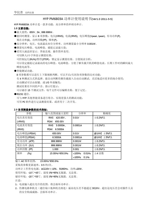
HYP PM6803A功率计使用说明书(Ver1.0 2011‐3‐5)HYP PM6803A功率计是一款多功能,高分辨率的单相功率计。
1.0主要功能:●最大量程:650V , 3A , 999.999W。
●能同时测量、显示8项参数:电压(VRMS), 电流(IRMS), 电压峰值(Vpeak, Ipeak), 有功功率(P),视在功率(S) , 功率因数(PF), 频率(F)。
●高分辨率:电压、电流最高5位分辨率,功率测量最小分辨率0.001W。
●测量电压峰值、电流峰值,捕捉记录最大值;●采用大液晶屏显示,界面直观,操作简单易用。
可切换大/小字体显示测量结果;可控制运行(RUN)/暂停(STOP),锁定显示测量结果,方便阅读分析;可以设定捕捉记录最高的电压峰值、电流峰值,方便了解负载开机的峰值电流、长期工作时的瞬间最大峰值电流等。
●智能测试功能。
8项参数都可以进行上下限规格判断,可以开启/关闭各项参数的比对功能;有4种测试方式供选择,能自动判断待测负载接入自动启动测试,灵活地适应更多的场合使用;启动测试可以由按键、或I/O外部触发;测试结果有不同的声音、指示灯提示;可以储存15个测试文件,每个文件可以编辑名称,便于记忆。
●RS232通信。
可与HYP其他智能设备进行组合,实现更强大的测试功能;可用PC软件进行记录测量结果,或者用于二次开发。
2.0各项测量参数的技术指标:参数 输入范围或最大量程 分辨率 精确度电压真有效值 (VRMS)RMS 420.00V ,PEAK 650.00V0.01V ±0.2%F.S.电流真有效值 (IRMS)RMS 3.0000A ,PEAK 6.5000A0.0001A ±0.2%F.S.电压峰值(VPEAK) 650.00V 0.01V @1KHZ ±5%F.S.电流峰值(IPEAK) 6.5000A 0.0001A @1KHZ ±5%F.S.有功功率 (ATP) 999.999W 0.001W ±0.2%F.S.视在功率 (SUI) 999.999W 0.001W ±0.2%F.S.功率因数 (PF) 1.000 0.001 ±0.2%F.S.频率 (Fq) 15.00Hz~650.0Hz <100Hz 0.01Hz>100Hz 0.1Hz±4读数输入AC频率范围: 15.00Hz~650.0Hz采集的参数更新速率:0.5秒/次。
AU6803 Twin PLL specifications ED3
5.3 Measures for Eliminating Noise 5.4 Constructing a Fail-safe System 5.5 Encoder Application Appendix Outline drawing of IC chip
--- --- --- --- --- --- --- --- --- --- --- --- --- --- --- ------ --- --- 30 --- --- --- --- --- --- --- --- --- --- --- --- --- --- --- ------ --- --- 31 --- --- --- --- --- --- --- --- --- --- --- --- --- --- --- --- --- --- --- 32
Setting register
Twin-PLL Smartcoder AU6803 Specifications Table of Contents
1. Scope 2. Related Documents 3. Requirements --- --- --- --- --- --- --- --- --- --- --- --- --- --- --- --- --- ------ --- --- 3 --- --- --- --- --- --- --- --- --- --- --- --- --- --- --- --- --- ------ --- --- 3 --- --- --- --- --- --- --- --- --- --- --- --- --- --- --- --- --- ------ --- --- 3 --- --- --- --- --- ------ --- --- --- --- --- --- --- --- --- --- -- 3
CY7C68013A中文资料

EZ-USB FX2LP™ USB MicrocontrollerCY7C68013A/CY7C68014A CY7C68015A/CY7C68016A1.0Features (CY7C68013A/14A/15A/16A)•USB 2.0–USB-IF high speed certified (TID # 40440111)•Single-chip integrated USB 2.0 transceiver, smart SIE, and enhanced 8051 microprocessor•Fit, form and function compatible with the FX2—Pin-compatible—Object-code-compatible—Functionally-compatible (FX2LP is a superset)•Ultra Low power: I CC no more than 85 mA in any mode —Ideal for bus and battery powered applications •Software: 8051 code runs from:—Internal RAM, which is downloaded via USB —Internal RAM, which is loaded from EEPROM —External memory device (128 pin package)•16 KBytes of on-chip Code/Data RAM•Four programmable BULK/INTERRUPT/ISOCHRO-NOUS endpoints—Buffering options: double, triple, and quad•Additional programmable (BULK/INTERRUPT) 64-byte endpoint•8- or 16-bit external data interface •Smart Media Standard ECC generation •GPIF (General Programmable Interface)—Allows direct connection to most parallel interface—Programmable waveform descriptors and configu-ration registers to define waveforms—Supports multiple Ready (RDY) inputs and Control (CTL) outputs•Integrated, industry-standard enhanced 8051—48-MHz, 24-MHz, or 12-MHz CPU operation —Four clocks per instruction cycle —Two USARTS—Three counter/timers—Expanded interrupt system —Two data pointers•3.3V operation with 5V tolerant inputs•Vectored USB interrupts and GPIF/FIFO interrupts •Separate data buffers for the Set-up and Data portions of a CONTROL transfer•Integrated I 2C controller, runs at 100 or 400 kHz •Four integrated FIFOs—Integrated glue logic and FIFOs lower system cost —Automatic conversion to and from 16-bit buses —Master or slave operation—Uses external clock or asynchronous strobes —Easy interface to ASIC and DSP ICs•Available in Commercial and Industrial temperature grade (all packages except VFBGA)A d d r e s s (16)x20PLL/0.5/1.0/2.08051 Core 12/24/48 MHz,four clocks/cycleI 2CVCC1.5kD+D–A d d r e s s (16) / D a t aB u s (8)FX2LPGPIFCY Smart USB 1.1/2.0EngineUSB 2.0XCVR16 KB RAM4 kB FIFOIntegrated full- and high-speedXCVRAdditional I/Os (24)ADDR (9)CTL (6)RDY (6)8/16D a t a (8)24 MHz Ext. XTALEnhanced USB core Simplifies 8051 code “Soft Configuration”Easy firmware changes FIFO and endpoint memory (master or slave operation)Up to 96 MBytes/s burst rateGeneralprogrammable I/F to ASIC/DSP or bus standards such as ATAPI, EPP , etc.Abundant I/Oincluding two USARTS High-performance micro using standard toolswith lower-power optionsMasterFigure 1-1. Block Diagramconnected for full speedECC1.1Features (CY7C68013A/14A only)•CY7C68014A: Ideal for battery powered applications —Suspend current: 100 µA (typ)•CY7C68013A: Ideal for non-battery powered applica-tions—Suspend current: 300 µA (typ)•Available in five lead-free packages with up to 40 GPIOs —128-pin TQFP (40 GPIOs), 100-pin TQFP (40 GPIOs),56-pin QFN (24 GPIOs), 56-pin SSOP (24 GPIOs), and 56-pin VFBGA (24 GPIOs)1.2Features (CY7C68015A/16A only)•CY7C68016A: Ideal for battery powered applications—Suspend current: 100 µA (typ)•CY7C68015A: Ideal for non-battery powered applica-tions—Suspend current: 300 µA (typ)•Available in lead-free 56-pin QFN package (26 GPIOs)—2 more GPIOs than CY7C68013A/14A enabling addi-tional features in same footprintCypress Semiconductor Corporation’s (Cypress’s) EZ-USB FX2LP™ (CY7C68013A/14A) is a low-power version of the EZ-USB FX2™ (CY7C68013), which is a highly integrated, low-power USB 2.0 microcontroller. By integrating the USB 2.0 transceiver, serial interface engine (SIE), enhanced 8051 microcontroller, and a programmable peripheral interface in a single chip, Cypress has created a very cost-effective solution that provides superior time-to-market advantages with low power to enable bus powered applications.The ingenious architecture of FX2LP results in data transfer rates of over 53 Mbytes per second, the maximum-allowable USB 2.0 bandwidth, while still using a low-cost 8051 microcon-troller in a package as small as a 56 VFBGA (5mm x 5mm). Because it incorporates the USB 2.0 transceiver, the FX2LP is more economical, providing a smaller footprint solution than USB 2.0 SIE or external transceiver implementations. With EZ-USB FX2LP, the Cypress Smart SIE handles most of the USB 1.1 and 2.0 protocol in hardware, freeing the embedded microcontroller for application-specific functions and decreasing development time to ensure USB compatibility. The General Programmable Interface (GPIF) and Master/Slave Endpoint FIFO (8- or 16-bit data bus) provides an easy and glueless interface to popular interfaces such as ATA, UTOPIA, EPP, PCMCIA, and most DSP/processors. The FX2LP draws considerably less current than the FX2 (CY7C68013), has double the on-chip code/data RAM and is fit, form and function compatible with the 56-, 100-, and 128-pin FX2.Five packages are defined for the family: 56VFBGA, 56 SSOP, 56 QFN, 100 TQFP, and 128 TQFP.2.0 Applications•Portable video recorder•MPEG/TV conversion•DSL modems•ATA interface•Memory card readers•Legacy conversion devices•Cameras•Scanners•Home PNA•Wireless LAN•MP3 players•NetworkingThe “Reference Designs” section of the Cypress web site provides additional tools for typical USB 2.0 applications. Each reference design comes complete with firmware source and object code, schematics, and documentation. Please visit for more information.3.0Functional Overview3.1USB Signaling SpeedFX2LP operates at two of the three rates defined in the USB Specification Revision 2.0, dated April 27, 2000:•Full speed, with a signaling bit rate of 12 Mbps •High speed, with a signaling bit rate of 480 Mbps.FX2LP does not support the low-speed signaling mode of 1.5Mbps.3.28051 MicroprocessorThe 8051 microprocessor embedded in the FX2LP family has 256 bytes of register RAM, an expanded interrupt system,three timer/counters, and two USARTs.3.2.18051 Clock FrequencyFX2LP has an on-chip oscillator circuit that uses an external 24-MHz (±100-ppm) crystal with the following characteristics:•Parallel resonant •Fundamental mode •500-µW drive level•12-pF (5% tolerance) load capacitors.An on-chip PLL multiplies the 24-MHz oscillator up to 480MHz, as required by the transceiver/PHY , and internal counters divide it down for use as the 8051 clock. The default 8051 clock frequency is 12 MHz. The clock frequency of the 8051 can be changed by the 8051 through the CPUCS register, dynamically.The CLKOUT pin, which can be three-stated and inverted using internal control bits, outputs the 50% duty cycle 8051clock, at the selected 8051 clock frequency—48, 24, or 12MHz.3.2.2USARTSFX2LP contains two standard 8051 USARTs, addressed via Special Function Register (SFR) bits. The USART interface pins are available on separate I/O pins, and are not multi-plexed with port pins.UART0 and UART1 can operate using an internal clock at 230KBaud with no more than 1% baud rate error. 230-KBaud operation is achieved by an internally derived clock source that generates overflow pulses at the appropriate time. The internal clock adjusts for the 8051 clock rate (48, 24, 12 MHz)such that it always presents the correct frequency for 230-KBaud operation.[1]3.2.3Special Function RegistersCertain 8051 SFR addresses are populated to provide fast access to critical FX2LP functions. These SFR additions are shown in Table 3-1. Bold type indicates non-standard,enhanced 8051 registers. The two SFR rows that end with “0”and “8” contain bit-addressable registers. The four I/O ports A–D use the SFR addresses used in the standard 8051 for ports 0–3, which are not implemented in FX2LP . Because of the faster and more efficient SFR addressing, the FX2LP I/O ports are not addressable in external RAM space (using the MOVX instruction).3.3I 2C BusFX2LP supports the I 2C bus as a master only at 100-/400-KHz.SCL and SDA pins have open-drain outputs and hysteresis inputs. These signals must be pulled up to 3.3V, even if no I 2C device is connected.3.4BusesAll packages: 8- or 16-bit “FIFO” bidirectional data bus, multi-plexed on I/O ports B and D. 128-pin package: adds 16-bit output-only 8051 address bus, 8-bit bidirectional data bus.Figure 3-1. Crystal Configuration12 pf12 pf24 MHz20 × PLLC1C212-pF capacitor values assumes a trace capacitanceof 3 pF per side on a four-layer FR4 PCANote:1.115-KBaud operation is also possible by programming the 8051 SMOD0 or SMOD1 bits to a “1” for UART0 and/or UART1, respectively.3.5USB Boot MethodsDuring the power-up sequence, internal logic checks the I2C port for the connection of an EEPROM whose first byte is either 0xC0 or 0xC2. If found, it uses the VID/PID/DID values in the EEPROM in place of the internally stored values (0xC0), or it boot-loads the EEPROM contents into internal RAM (0xC2). If no EEPROM is detected, FX2LP enumerates using internally stored descriptors. The default ID values for FX2LP are VID/PID/DID (0x04B4, 0x8613, 0xAxxx where xxx = Chip revision).[2]3.6ReNumeration™Because the FX2LP’s configuration is soft, one chip can take on the identities of multiple distinct USB devices.When first plugged into USB, the FX2LP enumerates automat-ically and downloads firmware and USB descriptor tables over the USB cable. Next, the FX2LP enumerates again, this time as a device defined by the downloaded information. This patented two-step process, called ReNumeration™, happens instantly when the device is plugged in, with no hint that the initial download step has occurred.Two control bits in the USBCS (USB Control and Status) register control the ReNumeration process: DISCON and RENUM. To simulate a USB disconnect, the firmware sets DISCON to 1. To reconnect, the firmware clears DISCON to 0. Before reconnecting, the firmware sets or clears the RENUM bit to indicate whether the firmware or the Default USB Device will handle device requests over endpoint zero: if RENUM = 0, the Default USB Device will handle device requests; if RENUM = 1, the firmware will.3.7Bus-powered ApplicationsThe FX2LP fully supports bus-powered designs by enumer-ating with less than 100 mA as required by the USB 2.0 speci-fication.3.8Interrupt System3.8.1INT2 Interrupt Request and Enable RegistersFX2LP implements an autovector feature for INT2 and INT4. There are 27 INT2 (USB) vectors, and 14 INT4 (FIFO/GPIF) vectors. See EZ-USB Technical Reference Manual (TRM) for more details.3.8.2USB-Interrupt AutovectorsThe main USB interrupt is shared by 27 interrupt sources. To save the code and processing time that normally would be required to identify the individual USB interrupt source, the FX2LP provides a second level of interrupt vectoring, called Autovectoring. When a USB interrupt is asserted, the FX2LP pushes the program counter onto its stack then jumps to address 0x0043, where it expects to find a “jump” instruction to the USB Interrupt service routine.Table 3-1. Special Function Registersx8x9x Ax Bx Cx Dx Ex Fx 0IOA IOB IOC IOD SCON1PSW ACC B 1SP EXIF INT2CLR IOE SBUF12DPL0MPAGE INT4CLR OEA3DPH0OEB4DPL1OEC5DPH1OED6DPS OEE7PCON8TCON SCON0IE IP T2CON EICON EIE EIP 9TMOD SBUF0A TL0AUTOPTRH1EP2468STAT EP01STAT RCAP2LB TL1AUTOPTRL1EP24FIFOFLGS GPIFTRIG RCAP2HC TH0reserved EP68FIFOFLGS TL2D TH1AUTOPTRH2GPIFSGLDATH TH2E CKCON AUTOPTRL2GPIFSGLDATLXF reserved AUTOPTRSET-UP GPIFSGLDATLNOXTable 3-2. Default ID Values for FX2LPDefault VID/PID/DIDVendor ID0x04B4Cypress SemiconductorProduct ID0x8613EZ-USB FX2LPDevice release0xAnnn Depends on chip revision(nnn = chip revision where firstsilicon = 001)Note:2.The I2C bus SCL and SDA pins must be pulled up, even if an EEPROM is not connected. Otherwise this detection method does not work properly.The FX2LP jump instruction is encoded as follows.If Autovectoring is enabled (AV2EN = 1 in the INTSET-UP register), the FX2LP substitutes its INT2VEC byte. Therefore, if the high byte (“page”) of a jump-table address is preloaded at location 0x0044, the automatically-inserted INT2VEC byte at 0x0045 will direct the jump to the correct address out of the 27 addresses within the page.3.8.3FIFO/GPIF Interrupt (INT4)Just as the USB Interrupt is shared among 27 individual USB-interrupt sources, the FIFO/GPIF interrupt is shared among 14 individual FIFO/GPIF sources. The FIFO/GPIF Interrupt, like the USB Interrupt, can employ autovectoring. Table3-4 shows the priority and INT4VEC values for the 14 FIFO/GPIF interrupt sources.Table 3-3. INT2 USB InterruptsUSB INTERRUPT TABLE FOR INT2 Priority INT2VEC Value Source Notes1 00SUDAV Set-up Data Available2 04 SOF Start of Frame (or microframe)3 08SUTOK Set-up Token Received4 0C SUSPEND USB Suspend request5 10USB RESET Bus reset6 14HISPEED Enteredhigh speed operation7 18 EP0ACK FX2LP ACK’d the CONTROL Handshake8 1C reserved9 20 EP0-IN EP0-IN ready to be loaded with data10 24 EP0-OUT EP0-OUT has USB data11 28 EP1-IN EP1-IN ready to be loaded with data12 2C EP1-OUT EP1-OUT has USB data13 30 EP2 IN: buffer available. OUT: buffer has data14 34 EP4 IN: buffer available. OUT: buffer has data15 38 EP6 IN: buffer available. OUT: buffer has data16 3C EP8 IN: buffer available. OUT: buffer has data17 40 IBN IN-Bulk-NAK (any IN endpoint)18 44reserved19 48 EP0PING EP0 OUT was Pinged and it NAK’d20 4C EP1PING EP1 OUT was Pinged and it NAK’d21 50 EP2PING EP2 OUT was Pinged and it NAK’d22 54 EP4PING EP4 OUT was Pinged and it NAK’d23 58 EP6PING EP6 OUT was Pinged and it NAK’d24 5C EP8PING EP8 OUT was Pinged and it NAK’d25 60 ERRLIMIT Bus errors exceeded the programmed limit26 6427 68 reserved28 6C reserved29 70 EP2ISOERR ISO EP2 OUT PID sequence error30 74 EP4ISOERR ISO EP4 OUT PID sequence error31 78 EP6ISOERR ISO EP6 OUT PID sequence error32 7C EP8ISOERR ISO EP8 OUT PID sequence errorIf Autovectoring is enabled (AV4EN = 1 in the INTSET-UP register), the FX 2LP substitutes its INT4VEC byte. Therefore, if the high byte (“page”) of a jump-table address is preloaded at location 0x0054, the automatically-inserted INT4VEC byte at 0x0055 will direct the jump to the correct address out of the 14 addresses within the page. When the ISR occurs, the FX2LP pushes the program counter onto its stack then jumps to address 0x0053, where it expects to find a “jump” instruction to the ISR Interrupt service routine.3.9Reset and Wakeup3.9.1Reset PinThe input pin, RESET#, will reset the FX2LP when asserted. This pin has hysteresis and is active LOW. When a crystal is used with the CY7C680xxA the reset period must allow for the stabilization of the crystal and the PLL. This reset period should be approximately 5 ms after VCC has reached 3.0V. If the crystal input pin is driven by a clock signal the internal PLL stabilizes in 200 µs after VCC has reached 3.0V[3]. Figure3-2 shows a power-on reset condition and a reset applied during operation. A power-on reset is defined as the time reset is asserted while power is being applied to the circuit. A powered reset is defined to be when the FX2LP has previously been powered on and operating and the RESET# pin is asserted. Cypress provides an application note which describes and recommends power on reset implementation and can be found on the Cypress web site. For more information on reset imple-mentation for the FX2 family of products visit the .Table 3-4. Individual FIFO/GPIF Interrupt SourcesPriority INT4VEC Value Source Notes 180EP2PF Endpoint 2 Programmable Flag2 84 EP4PF Endpoint 4 Programmable Flag388EP6PF Endpoint 6 Programmable Flag48C EP8PF Endpoint 8 Programmable Flag590EP2EF Endpoint 2 Empty Flag694EP4EF Endpoint 4 Empty Flag798EP6EF Endpoint 6 Empty Flag89C EP8EF Endpoint 8 Empty Flag9A0 EP2FF Endpoint 2 Full Flag10A4EP4FF Endpoint 4 Full Flag11 A8EP6FF Endpoint 6 Full Flag12AC EP8FF Endpoint 8 Full Flag13 B0GPIFDONE GPIF Operation Complete14 B4GPIFWF GPIF WaveformNote:3.If the external clock is powered at the same time as the CY7C680xxA and has a stabilization wait period, it must be added to the 200 µs.3.9.2Wakeup PinsThe 8051 puts itself and the rest of the chip into a power-down mode by setting PCON.0 = 1. This stops the oscillator and PLL. When WAKEUP is asserted by external logic, the oscil-lator restarts, after the PLL stabilizes, and then the 8051receives a wakeup interrupt. This applies whether or not FX2LP is connected to the USB.The FX2LP exits the power-down (USB suspend) state using one of the following methods:•USB bus activity (if D+/D– lines are left floating, noise on these lines may indicate activity to the FX2LP and initiate a wakeup).•External logic asserts the WAKEUP pin •External logic asserts the PA3/WU2 pin.The second wakeup pin, WU2, can also be configured as a general purpose I/O pin. This allows a simple external R-C network to be used as a periodic wakeup source. Note that WAKEUP is by default active LOW.3.10Program/Data RAM3.10.1SizeThe FX2LP has 16 KBytes of internal program/data RAM,where PSEN#/RD# signals are internally ORed to allow the 8051 to access it as both program and data memory. No USB control registers appear in this space.Two memory maps are shown in the following diagrams:Figure 3-3 Internal Code Memory, EA = 0Figure 3-4 External Code Memory, EA = 1.3.10.2Internal Code Memory, EA = 0This mode implements the internal 16-KByte block of RAM (starting at 0) as combined code and data memory. When external RAM or ROM is added, the external read and write strobes are suppressed for memory spaces that exist inside the chip. This allows the user to connect a 64-KByte memory without requiring address decodes to keep clear of internal memory spaces.Only the internal 16 KBytes and scratch pad 0.5 KBytes RAM spaces have the following access:•USB download •USB upload •Set-up data pointer •I 2C interface boot load.3.10.3External Code Memory, EA = 1The bottom 16 KBytes of program memory is external, and therefore the bottom 16 KBytes of internal RAM is accessible only as data memory.Figure 3-2. Reset Timing PlotsV IL 0V3.3V 3.0VT RESETVCCRESET#Power on ResetT RESETVCCRESET#V IL Powered Reset3.3V0VTable 3-5. Reset Timing ValuesConditionT RESET Power-on Reset with crystal 5 msPower-on Reset with external clock200 µs + Clock stability timePowered Reset 200 µsFigure 3-3. Internal Code Memory, EA = 0Inside FX2LPOutside FX2LP7.5 KBytes USB regs and 4K FIFO buffers (RD#,WR#)0.5 KBytes RAM Data (RD#,WR#)*(OK to populate data memory here—RD#/WR#strobes are not active)40 KBytes External Data Memory (RD#,WR#)(Ok to populate data memory here—RD#/WR#strobes are not active)16 KBytes RAM Code and Data(PSEN#,RD#,WR#)*48 KBytes External Code Memory (PSEN#)(OK to populate programmemory here—PSEN# strobe is not active)*SUDPTR, USB upload/download, I 2C interface boot accessFFFFE200E1FF E0003FFF0000DataCodeFigure 3-4. External Code Memory, EA = 1Inside FX2LPOutside FX2LP7.5 KBytes USB regs and 4K FIFO buffers (RD#,WR#)0.5 KBytes RAM Data (RD#,WR#)*(OK to populatedata memory here—RD#/WR#strobes are not active)40 KBytes External Data Memory (RD#,WR#)(Ok to populate data memory here—RD#/WR#strobes are not active)16 KBytes RAM Data(RD#,WR#)*64 KBytes External Code Memory (PSEN#)*SUDPTR, USB upload/download, I 2C interface boot accessFFFFE200E1FFE0003FFF0000DataCode3.11Register Addresses3.12Endpoint RAM3.12.1Size•3× 64 bytes (Endpoints 0 and 1)•8 × 512 bytes (Endpoints 2, 4, 6, 8)3.12.2Organization•EP0•Bidirectional endpoint zero, 64-byte buffer •EP1IN, EP1OUT•64-byte buffers, bulk or interrupt •EP2,4,6,8•Eight 512-byte buffers, bulk, interrupt, or isochronous. EP4 and EP8 can be double buffered, while EP2 and 6 can be either double, triple, or quad buffered. For high-speed end-point configuration options, see Figure 3-5.3.12.3Set-up Data BufferA separate 8-byte buffer at 0xE6B8-0xE6BF holds the Set-up data from a CONTROL transfer.3.12.4Endpoint Configurations (High-speed Mode)Endpoints 0 and 1 are the same for every configuration.Endpoint 0 is the only CONTROL endpoint, and endpoint 1 can be either BULK or INTERRUPT. The endpoint buffers can be configured in any 1 of the 12 configurations shown in the vertical columns. When operating in full-speed BULK mode only the first 64 bytes of each buffer are used. For example in high-speed, the max packet size is 512 bytes but in full-speed it is 64 bytes. Even though a buffer is configured to be a 512byte buffer, in full-speed only the first 64 bytes are used. The unused endpoint buffer space is not available for other opera-tions. An example endpoint configuration would be:FFFFE800E7BF E740E73F E700E6FF E500E4FF E480E47F E400E200E1FFE000E3FF EFFF2 KBytes RESERVED64 Bytes EP0 IN/OUT 64 Bytes RESERVED 8051 Addressable RegistersReserved (128)128 bytes GPIF Waveforms512 bytes 8051 xdata RAMF000(512)Reserved (512)E78064 Bytes EP1OUT E77F 64 Bytes EP1IN E7FF E7C0 4 KBytes EP2-EP8buffers(8 x 512)EP2–1024 double buffered; EP6–512 quad buffered (column 8).3.12.5Default Full-Speed Alternate Settings3.12.6Default High-Speed Alternate Settings6464645125121024102410241024102410241024512512512512512512512512512512EP0 IN&OUTEP1 IN EP1 OUTFigure 3-5. Endpoint Configuration1024102410245125125125125125125125125125125125125125125125125125125125125125125125125125125125125125121024102410241024102410245125121024102451251251251251251251251210241024512512512512512512646464646464646464646464646464646464646464646464646464646464646464123456789101112Table 3-6. Default Full-Speed Alternate Settings [4, 5]Alternate Setting 0123ep064646464ep1out 064 bulk 64 int 64 int ep1in 064 bulk 64 int 64 int ep2064 bulk out (2×)64 int out (2×)64 iso out (2×)ep4064 bulk out (2×)64 bulk out (2×)64 bulk out (2×)ep6064 bulk in (2×)64 int in (2×)64 iso in (2×)ep8064 bulk in (2×)64 bulk in (2×)64 bulk in (2×)Notes:4.“0” means “not implemented.”5.“2×” means “double buffered.”6.Even though these buffers are 64 bytes, they are reported as 512 for USB 2.0 compliance. The user must never transfer packets larger than 64 bytes to EP1.Table 3-7. Default High-Speed Alternate Settings [4, 5]Alternate Setting 0123ep064646464ep1out 0512 bulk [6]64 int 64 int ep1in 0512 bulk [6]64 int64 intep20512 bulk out (2×)512 int out (2×)512 iso out (2×)ep40512 bulk out (2×)512 bulk out (2×)512 bulk out (2×)ep60512 bulk in (2×)512 int in (2×)512 iso in (2×)ep80512 bulk in (2×)512 bulk in (2×)512 bulk in (2×)3.13External FIFO Interface3.13.1ArchitectureThe FX2LP slave FIFO architecture has eight 512-byte blocks in the endpoint RAM that directly serve as FIFO memories, and are controlled by FIFO control signals (such as IFCLK, SLCS#, SLRD, SLWR, SLOE, PKTEND, and flags).In operation, some of the eight RAM blocks fill or empty from the SIE, while the others are connected to the I/O transfer logic. The transfer logic takes two forms, the GPIF for internally generated control signals, or the slave FIFO interface for externally controlled transfers.3.13.2Master/Slave Control SignalsThe FX2LP endpoint FIFOS are implemented as eight physi-cally distinct 256x16 RAM blocks. The 8051/SIE can switch any of the RAM blocks between two domains, the USB (SIE) domain and the 8051-I/O Unit domain. This switching is done virtually instantaneously, giving essentially zero transfer time between “USB FIFOS” and “Slave FIFOS.” Since they are physically the same memory, no bytes are actually transferred between buffers.At any given time, some RAM blocks are filling/emptying with USB data under SIE control, while other RAM blocks are available to the 8051 and/or the I/O control unit. The RAM blocks operate as single-port in the USB domain, and dual-port in the 8051-I/O domain. The blocks can be configured as single, double, triple, or quad buffered as previ-ously shown.The I/O control unit implements either an internal-master (M for master) or external-master (S for Slave) interface.In Master (M) mode, the GPIF internally controls FIFOADR[1..0] to select a FIFO. The RDY pins (two in the 56-pin package, six in the 100-pin and 128-pin packages) can be used as flag inputs from an external FIFO or other logic if desired. The GPIF can be run from either an internally derived clock or externally supplied clock (IFCLK), at a rate that transfers data up to 96 Megabytes/s (48-MHz IFCLK with 16-bit interface).In Slave (S) mode, the FX2LP accepts either an internally derived clock or externally supplied clock (IFCLK, max. frequency 48 MHz) and SLCS#, SLRD, SLWR, SLOE, PKTEND signals from external logic. When using an external IFCLK, the external clock must be present before switching to the external clock with the IFCLKSRC bit. Each endpoint can individually be selected for byte or word operation by an internal configuration bit, and a Slave FIFO Output Enable signal SLOE enables data of the selected width. External logic must insure that the output enable signal is inactive when writing data to a slave FIFO. The slave interface can also operate asynchronously, where the SLRD and SLWR signals act directly as strobes, rather than a clock qualifier as in synchronous mode. The signals SLRD, SLWR, SLOE and PKTEND are gated by the signal SLCS#.3.13.3GPIF and FIFO Clock RatesAn 8051 register bit selects one of two frequencies for the internally supplied interface clock: 30 MHz and 48 MHz. Alter-natively, an externally supplied clock of 5 MHz–48 MHz feeding the IFCLK pin can be used as the interface clock. IFCLK can be configured to function as an output clock when the GPIF and FIFOs are internally clocked. An output enable bit in the IFCONFIG register turns this clock output off, if desired. Another bit within the IFCONFIG register will invert the IFCLK signal whether internally or externally sourced. 3.14GPIFThe GPIF is a flexible 8- or 16-bit parallel interface driven by a user-programmable finite state machine. It allows the CY7C68013A/15A to perform local bus mastering, and can implement a wide variety of protocols such as ATA interface, printer parallel port, and Utopia.The GPIF has six programmable control outputs (CTL), nine address outputs (GPIFADRx), and six general-purpose ready inputs (RDY). The data bus width can be 8 or 16 bits. Each GPIF vector defines the state of the control outputs, and deter-mines what state a ready input (or multiple inputs) must be before proceeding. The GPIF vector can be programmed to advance a FIFO to the next data value, advance an address, etc. A sequence of the GPIF vectors make up a single waveform that will be executed to perform the desired data move between the FX2LP and the external device.3.14.1Six Control OUT SignalsThe 100- and 128-pin packages bring out all six Control Output pins (CTL0-CTL5). The 8051 programs the GPIF unit to define the CTL waveforms. The 56-pin package brings out three of these signals, CTL0–CTL2. CTLx waveform edges can be programmed to make transitions as fast as once per clock (20.8 ns using a 48-MHz clock).3.14.2Six Ready IN SignalsThe 100- and 128-pin packages bring out all six Ready inputs (RDY0–RDY5). The 8051 programs the GPIF unit to test the RDY pins for GPIF branching. The 56-pin package brings out two of these signals, RDY0–1.3.14.3Nine GPIF Address OUT SignalsNine GPIF address lines are available in the 100- and 128-pin packages, GPIFADR[8..0]. The GPIF address lines allow indexing through up to a 512-byte block of RAM. If more address lines are needed, I/O port pins can be used.3.14.4Long Transfer ModeIn master mode, the 8051 appropriately sets GPIF transaction count registers (GPIFTCB3, GPIFTCB2, GPIFTCB1, or GPIFTCB0) for unattended transfers of up to 232 transactions. The GPIF automatically throttles data flow to prevent under or overflow until the full number of requested transactions complete. The GPIF decrements the value in these registers to represent the current status of the transaction.。
AN001(1)6803角度方案
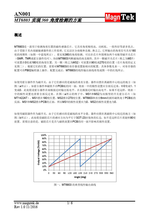
概述MT6803是一款用于检测角度位置的磁传感器芯片。
它具有角度精度高、功耗低、一致性好等诸多优点。
由于受限于其内部磁敏感器件的工作原理,它无法区分南极和北极。
换言之,它所输出的角度信号具有180度的周期性(如图一中蓝线所示)。
要实现360的角度检测,可以在芯片外围增加两个双极型磁开关芯片(GMR、TMR或霍尔器件均可),协助MT6803判断磁场的南北极性。
其中一颗磁开关芯片(称之为MS1)可放置在0度或180度的角度位置,另一颗(称之为MS2)可放置在90度或270度的位置(芯片角度的定义见图二)。
根据它们的位置,需要对MT6803的寄存器设置做相应的配置,具体参数见表一。
对寄存器的配置可在PB02编程器上操作。
配置完成后,MT6803的线性输出曲线将变成图一中的红线所示。
如使用霍尔器件作为磁开关,由于它们感应的是磁场的垂直分量,器件应摆在离磁铁中心较远的地方(如图三a所示)。
如霍尔器件和磁铁不在PCB板的同一面,则表一中的极性设置应全部反过来,即0变成1,1变成0。
此处假设霍尔器件在南极接近时输出低电平,在北极接近时输出高电平。
如果不是这样,则表一中的极性设置也需要全部反过来。
在图三a所示的例子中,MS1和MS2为双极型的开关霍尔芯片(如MT1422AT),MS1摆在180度位置,MS2摆在270度位置。
MT6803和直径6mm的圆形磁铁处于PCB板的反面,MS1和MS2摆在PCB的正面,所以MS1的极性设置应为0,MS2的极性设置也为0。
如使用磁阻器件作为磁开关,由于它们感应的是磁场的水平分量,器件应摆在离磁铁中心较近的地方(如图三b所示)。
此处假设磁阻芯片的感应方向为平行于SOT-23封装体的长边,如不是这样芯片需旋转90度放置。
需要注意的是,磁阻芯片是否与磁铁放置在PCB的同一面不影响其极性设置。
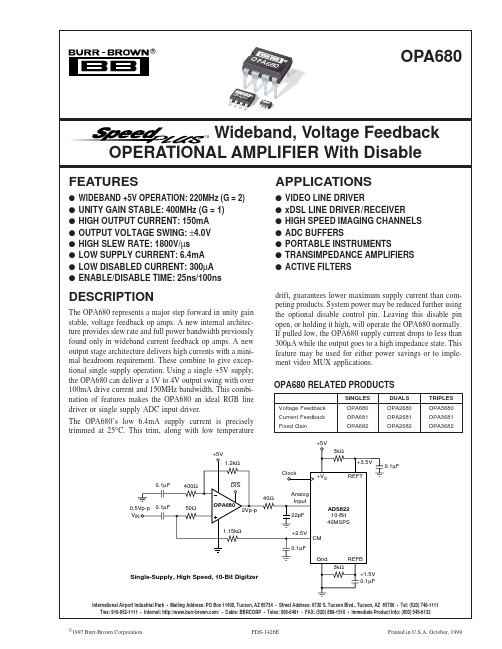
图一:MT6803的典型线性输出曲线α图二:芯片的敏感区域标示,各个角度位置的定义表一:(a)(b)图三:一种可能的放置情况(MT6803和磁铁在PCB板的背面,磁开关芯片在PCB板的正面)(a)用霍尔器件的情况;(b)用磁阻器件的情况。
医疗器械常用词汇中英文对照

55
680707
Ⅱ类
胸腔心血管外科用吸引器 thoracic cavity cardiovascular surgical aspirator
56 6808
腹部外科手术器械 abdominal surgical operation instruments
57
680802
Ⅰ类
腹部外科用剪 abdominal surgical scissors
2
680101
Ⅱ类
医用缝合针(不带线) medical suture needle (without thread)
3
680102
Ⅰ类
基础外科用刀 basic surgical knife
4
680103
Ⅰ类
基础外科用剪 basic surgical scissors
5
680104
Ⅰ类
基础外科用钳 basic surgical clamp
医疗器械产品分类目 Medical Equipment Classific
监管类
序 号 Ser ial NO.
分类 编码 Class ifica tion Code
别 Superv ision
& Admini strati
on
Level
名称 Name
1 6801
基础外科手术器械 basic surgical operation instruments
83
681202
Ⅰ类
妇产科用剪 obsteric and gynecologic scissors
84
681203
Ⅰ类
妇产科用钳 obsteric and gynecologic forceps