HDSP-5703-HG000中文资料
XXHDS产品优势介绍yx

HPQ XP256 XP48 XP512 XP128 XP1024 XP10000 XP12000 XP 24000
SUN N/A SE9910 SE9960 SE9970 SE9980 SE9985 SE9990 SE9990V
学习改变命运,知 识创造未来
XXHDS产品优势介绍yx
各厂商磁盘产品
• HDS独有虚拟端口模式
– 每一个物理端口支持128个异构主机 平台连接
• 各主机拥有自己的存储空间,没有数 据覆盖危险
• 多个LUN 0 支持
– 更好的利用FC端口200MB/s的带宽
• 很多应用仅需要5-10MB/s的带宽
学习改变命运,知 识创造未来
•存储系统
•POR T
•AMS •Virtual Port
SE9985
SE9990
SE9990 V
• HP:高端存储全球OEM战略合作 • SUN:高端存储全球联合品牌合作 • 联想、Gateway、Acer:中、低端模
块化存储联合品牌
学习改变命运,知 识创造未来
•直销 •代理商
•OEMs
•直销
•分销
XXHDS产品优势介绍yx
•代理商
•OE M
HDS中国区业务
• 4 iSCSI ports—2 per controller (Fibre Channel models available 2008)
• Supports SATA II (500GB or 750GB) or SAS (147GB or 300GB) HDDs
• 6, 8, or 12 HDDs per model, up to 9TB of capacity
• • • •
HDSP-G10X资料

Features• Low Power Consumption • Industry Standard Size• Industry Standard Pinout • Choice of Character Size 7.6 mm (0.30 in), 10 mm (0.40 in), 10.9 mm (0.43 in), 14.2 mm (0.56 in), 20 mm (0.80 in)• Choice of ColorsAlGaAs Red, High Efficiency Red (HER), Yellow, Green• Excellent Appearance Evenly Lighted Segments±50° Viewing Angle• Design FlexibilityCommon Anode or Common CathodeSingle and Dual DigitLeft and Right Hand Decimal Points±1. Overflow Character• Categorized for Luminous IntensityYellow and Green Categorized for ColorUse of Like Categories Yields a Uniform Display• Excellent for Long Digit String Multiplexing DescriptionThese low current seven segment displays are designed for applica-tions requiring low power consumption. They are tested and selected for their excellent low current characteristics to ensure that the segments are matched at low currents. Drive currents as low as 1 mA per segment are available.Pin for pin equivalent displays are also available in a standard current or high light ambient design. The standard current displays are available in all colors and are ideal for most applica-tions. The high light ambient displays are ideal for sunlight ambients or long string lengths. For additional information see the 7.6 mm Micro Bright Seven Segment Displays, 10 mm Seven Segment Displays, 7.6 mm/10.9 mm Seven Segment Displays, 14.2 mm Seven Segment Displays, 20 mm Seven Segment Displays, or High Light Ambient Seven Segment Displays data sheets.Low Current Seven SegmentDisplays Technical Data HDSP-335x Series HDSP-555x Series HDSP-751x Series HDSP-A10x Series HDSP-A80x Series HDSP-A90x Series HDSP-E10x Series HDSP-F10x Series HDSP-G10x Series HDSP-H10x Series HDSP-K12x, K70x SeriesHDSP-N10x SeriesDevicesAlGaAs HER Yellow Green Package HDSP-HDSP-HDSP-HDSP-Description Drawing A1017511A801A9017.6 mm Common Anode Right Hand Decimal AA1037513A803A9037.6 mm Common Cathode Right Hand Decimal BA1077517A807A9077.6 mm Common Anode ±1. Overflow CA1087518A808A9087.6 mm Common Cathode ±1. Overflow DF10110 mm Common Anode Right Hand Decimal EF10310 mm Common Cathode Right Hand Decimal FF10710 mm Common Anode ±1. Overflow GF10810 mm Common Cathode ±1. Overflow HG10110 mm Two Digit Common Anode Right Hand Decimal XG10310 mm Two Digit Common Cathode Right Hand Decimal YE100335010.9 mm Common Anode Left Hand Decimal IE101335110.9 mm Common Anode Right Hand Decimal JE103335310.9 mm Common Cathode Right Hand Decimal KE106335610.9 mm Universal ±1. Overflow[1]LH101555114.2 mm Common Anode Right Hand Decimal MH103555314.2 mm Common Cathode Right Hand Decimal NH107555714.2 mm Common Anode ±1. Overflow OH108555814.2 mm Common Cathode ±1. Overflow PK121K70114.2 mm Two Digit Common Anode Right Hand Decimal RK123K70314.2 mm Two Digit Common Cathode Right Hand Decimal SN10020 mm Common Anode Left Hand Decimal QN10120 mm Common Anode Right Hand Decimal TN10320 mm Common Cathode Right Hand Decimal UN10520 mm Common Cathode Left Hand Decimal VN10620 mm Universal ±1. Overflow[1]W Note:1. Universal pinout brings the anode and cathode of each segment’s LED out to separate pins. See internal diagrams L or W.Part Numbering System5082-x xx x-x x x xxHDSP-x xx x-x x x xxMechanical Options[1]00: No mechanical optionColor Bin Options[1,2]0: No color bin limitationMaximum Intensity Bin[1,2]0: No maximum intensity bin limitationMinimum Intensity Bin[1,2]0: No minimum intensity bin limitationDevice Configuration/Color[1]G: GreenDevice Specific Configuration[1]Refer to respective datasheetPackage[1]Refer to Respective datasheetNotes:1. For codes not listed in the figure above, please refer to the respective datasheet or contact your nearest Agilent representative fordetails.2. Bin options refer to shippable bins for a part-number. Color and Intensity Bins are typically restricted to 1 bin per tube (excep-tions may apply). Please refer to respective datasheet for specific bin limit information.Package DimensionsPackage Dimensions (cont.)Package Dimensions (cont.)*The Side View of package indicates Country of Origin.Package Dimensions (cont.)Package Dimensions (cont.)元器件交易网9 Package Dimensions (cont.)10 Internal Circuit DiagramInternal Circuit Diagram (cont.)Absolute Maximum RatingsAlGaAs Red HERHDSP-A10X/E10X/HDSP-751X/Yellow GreenH10X/K12X/N10X/335X/555X/HDSP-A80X HDSP-A90X Description F10X, G10X Series K70X Series Series Series Units Average Power per Segment or DP375264mW Peak Forward Current per 45mA Segment or DPDC Forward Current per15[1]15[2]mA Segment or DPOperating Temperature Range-20 to +100-40 to +100°C Storage Temperature Range -55 to +100°C Reverse Voltage per Segment 3.0V or DPLead Solder Temperature for 3Seconds (1.60 mm [0.063 in.] below 260°C seating plane)Notes:1. Derate above 91°C at 0.53 mA/°C.2. Derate HER/Yellow above 80°C at 0.38 mA/°C and Green above 71°C at 0.31 mA/°C.Electrical/Optical Characteristics at T A = 25°CAlGaAs RedDeviceSeriesHDSP-Parameter Symbol Min.Typ.Max.Units Test Conditions315600I F = 1 mA A10x3600I F = 5 mA330650I F = 1 mAF10x, G10x3900I F = 5 mA390650I F = 1 mA E10x Luminous Intensity/Segment[1,2]I Vµcd(Digit Average)3900I F = 5 mA400700I F = 1 mAH10x, K12x4200I F = 5 mA270590I F = 1 mA N10x3500I F = 5 mA1.6I F = 1 mAForward Voltage/Segment or DP V F 1.7V I F = 5 mA1.82.2I F = 20 mA Pk All Devices Peak WavelengthλPEAK645nmDominant Wavelength[3]λd637nmReverse Voltage/Segment or DP[4]V R 3.015V I R = 100 µATemperature Coefficient of∆V F/°C-2 mV mV/°CV F/Segment or DPA10x255F10x, G10x320E10x340Thermal Resistance LED RθJ-PIN°C/W/SegH10x, K12x Junction-to-Pin400N10x430High Efficiency RedDeviceSeriesHDSP-Parameter Symbol Min.Typ.Max.Units Test Conditions160270I F = 2 mA 751x1050I F = 5 mA200300I F = 2 mA Luminous Intensity/Segment[1,2]I V mcd(Digit Average)1200I F = 5 mA335x, 555x,K70x270370I F = 2 mA1480I F = 5 mA1.6I F = 2 mAForward Voltage/Segment or DP V F 1.7V I F = 5 mA2.1 2.5I F = 20 mA Pk All Devices Peak WavelengthλPEAK635nmDominant Wavelength[3]λd626nmReverse Voltage/Segment or DP[4]V R 3.030V I R = 100 µATemperature Coefficient of∆V F/°C-2mV/°CV F/Segment or DP751x200335x Thermal Resistance LED RθJ-PIN280°C/WJunction-to-Pin555x, K70x345YellowDeviceSeriesHDSP-Parameter Symbol Min.Typ.Max.Units Test Conditions Luminous Intensity/Segment[1,2]250420I F = 4 mA(Digit Average)I V mcd1300I F = 10 mA1.7I F = 4 mAForward Voltage/Segment or DP V F 1.8V I F = 5 mA A80x2.1 2.5I F = 20 mA PkPeak WavelengthλPEAK583nmDominant Wavelength[3,5]λd581.5585592.5nmReverse Voltage/Segment or DP[4]V R 3.030V I R = 100 µATemperature Coefficient of∆V F/°C-2mV/°CV F/Segment or DPThermal Resistance LED RθJ-PIN200°C/WJunction-to-PinGreenDeviceSeriesHDSP-Parameter Symbol Min.Typ.Max.Units Test Conditions Luminous Intensity/Segment[1,2]250475I F = 4 mA(Digit Average)I V mcd1500I F = 10 mA1.9I F = 4 mAForward Voltage/Segment or DP V F 2.0V I F = 10 mA A90x2.1 2.5I F = 20 mA PkPeak WavelengthλPEAK566nmDominant Wavelength[3,5]λd571577nmReverse Voltage/Segment or DP[4]V R 3.030V I R = 100 µATemperature Coefficient of∆V F/°C-2mV/°CV F/Segment or DPThermal Resistance LED RθJ-PIN200°C/WJunction-to-PinNotes:1. Device case temperature is 25°C prior to the intensity measurement.2. The digits are categorized for luminous intensity. The intensity category is designated by a letter on the side of the package.3. The dominant wavelength, λd, is derived from the CIE chromaticity diagram and is the single wavelength which defines the color of thedevice.4. Typical specification for reference only. Do not exceed absolute maximum ratings.5. The yellow (HDSP-A800) and Green (HDSP-A900) displays are categorized for dominant wavelength. The category is designated by anumber adjacent to the luminous intensity category letter.Intensity Bin Limits (mcd)AlGaAs RedHDSP-A10xIV Bin Category Min.Max.E0.3150.520F0.4280.759G0.621 1.16H0.945 1.71I 1.40 2.56J 2.10 3.84K 3.14 5.75L 4.708.55HDSP-E10x/F10x/G10xIV Bin Category Min.Max.D0.3910.650E0.5320.923F0.755 1.39G 1.13 2.08H 1.70 3.14HDSP-H10x/K12xIV Bin Category Min.Max.C0.4150.690D0.5650.990E0.810 1.50F 1.20 2.20G 1.80 3.30H 2.73 5.00I 4.097.50HDSP-N10xIV Bin Category Min.Max.A0.2700.400B0.3250.500C0.4150.690D0.5650.990E0.810 1.50F 1.20 2.20G 1.80 3.30H 2.73 5.00I 4.097.50Intensity Bin Limits (mcd), continued HERHDSP-751xIV Bin Category Min.Max.B0.1600.240C0.2000.300D0.2500.385E0.3150.520F0.4280.759G0.621 1.16HDSP-751xIV Bin Category Min.Max.B0.2400.366C0.3000.477D0.3910.650E0.5320.923F0.755 1.39G 1.13 2.08H 1.70 3.14HDSP-555x/K70xIV Bin Category Min.Max.A0.2700.400B0.3250.500C0.4150.690D0.5650.990E0.810 1.50F 1.20 2.20G 1.80 3.30H 2.73 5.00I 4.097.50Intensity Bin Limits (mcd), continued YellowHDSP-A80xIV Bin Category Min.Max.D0.2500.385E0.3150.520F0.4250.760G0.625 1.14H0.940 1.70I 1.40 2.56J 2.10 3.84K 3.14 5.76L 4.718.64M7.0713.00N10.6019.40O15.9029.20P23.9043.80Q35.8065.60GreenHDSP-A90xIV Bin Category Min.Max.E0.3150.520F0.4250.760G0.625 1.14H0.940 1.70I 1.40 2.56J 2.10 3.84K 3.14 5.76L 4.718.64M7.0713.00N10.6019.40O15.9029.20P23.9043.80Q35.8065.60Electrical/OpticalFor more information on electrical/optical characteristics, please see Application Note 1005.Contrast Enhancement For information on contrast enhancement, please see Application Note 1015.Soldering/Cleaning Cleaning agents from the ketone family (acetone, methyl ethyl ketone, etc.) and from the chorinated hydrocarbon family (methylene chloride, trichloro-ethylene, carbon tetrachloride, etc.) are not recommended for cleaning LED parts. All of these various solvents attack or dissolve the encapsulating epoxies used to form the package of plastic LED parts.For information on soldering LEDs, please refer to Application Note 1027.Note:All categories are established for classification of products. Productsmay not be available in all categories. Please contact your localAgilent representatives for further clarification/information.Color Categories/semiconductorsFor product information and a complete list ofdistributors, please go to our web site.For technical assistance call:Americas/Canada: +1 (800) 235-0312 or(916) 788 6763Europe: +49 (0) 6441 92460China: 10800 650 0017Hong Kong: (+65) 6271 2451India, Australia, New Zealand: (+65) 6271 2394Japan: (+81 3) 3335-8152(Domestic/International), or0120-61-1280(Domestic Only)Korea: (+65) 6271 2194Malaysia, Singapore: (+65) 6271 2054Taiwan: (+65) 6271 2654Data subject to change.Copyright © 2003 Agilent Technologies, Inc.Obsoletes 5988-8412ENSeptember 24, 20035989-0080EN。
HDSP-0883-00300中文资料

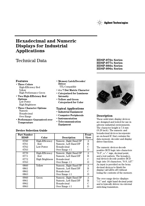
DevicesPart Number HDSP-ColorDescriptionFront View0781High-Efficiency Red Numeric, Right Hand DP A 0782Low Power Numeric, Left Hand DP B 0783Over Range ±1C 0784HexadecimalD 0791High-Efficiency Red Numeric, Right Hand DP A 0792High Brightness Numeric, Left Hand DP B 0793Over Range ±1C 0794HexadecimalD 0881YellowNumeric, Right Hand DP A 0882Numeric, Left Hand DP B 0883Over Range ±1C 0884HexadecimalD 0981High-Performance GreenNumeric, Right Hand DP A 0982Numeric, Left Hand DP B 0983Over Range ±1C 0984HexadecimalDHDSP-078x HDSP-079x HDSP-088x HDSP-098xFeatures• Three Character Options Numeric, Hexadecimal, Over Range• Three ColorsHigh Efficiency Red, Yellow,High Performance Green• 4x 7 Dot Matrix Character • High Efficiency Red, Yellow and High Performance Green • Two High Efficiency Red OptionsLow Power, High Brightness • Performance Guaranteed Over Temperature• High Temperature Stabilized • Memory Latch/Decoder/DriverTTL Compatible• Categorized for Luminous IntensityDescriptionThese standard solid state displays have a 7.4 mm (0.29 inch) dot matrix character and an on-board IC with data memory latch/decoder and LED drivers in a glass/ceramic package.The hermetic HDSP-078x,-079x/-088x displays utilize a solder glass frit seal. The HDSP-098X displays utilize an epoxy glass-to-ceramic seal.The numeric devices decode posi-tive BCD logic into characters “0-9,” a “–” sign, decimal point,and a test pattern. Thehexadecimal devices decodeGlass/Ceramic Numeric and Hexadecimal Displays for Industrial Applications Technical Datapositive BCD logic into 16characters, “0-9, A-F.” An input is provided on the hexadecimal devices to blank the display (all LEDS off) without losing the contents of the memory.The over range device displays “±1” and right hand decimal point and is typically driven via external switching transistors.COUNTRY CODEPackage DimensionsAbsolute Maximum RatingsNotes:1. The nominal thermal resistance of a display mounted in a socket that is soldered onto a printed circuit board isRθJA=50°C/W/device. The device package thermal resistance is RθJ-PIN = 15°C/W/device. The thermal resistance device pin-to-ambient through the PC board should not exceed 35°C/W/device for operation up to T A = +100°C.2. Voltage values are with respect to device ground, pin 6.3. These displays are categorized for luminous intensity with the intensity category designated by a letter code located on the back ofthe display package. Case temperature of the device immediately prior to the light measurement is equal to 25°C.Electrical/Optical Characteristics T A = –55°C to +100°CNotes:4. The luminous intensity at a specific operating ambienttemperature, I v(T A), may be approximated from the following exponential equation: I v(T A)=I v(25°C) e[k(T-25°C)].Device KHDSP-078 Series–0.0131/°CHDSP-079x SeriesHDSP-088x Series–0.0112/°CHDSP-098x Series–0.0104/°C 5. The dominant wavelength, λd, is derived from the CIE chroma-ticity diagram and represents the single wavelength whichdefines the color of the device.6. The HDSP-088X and HDSP-098X series devices are categor-ized as to dominant wavelength with the category designated by a number on the back of the display package.7. All typical values at V CC = 5.0 V and T A = 25°C.Operational ConsiderationsElectricalThese devices use a modified4x7 dot matrix of light emitting diodes to display decimal/ hexadecimal numeric informa-tion. The high efficiency red and yellow displays use GaAsP/GaP LEDs and the high performance green displays use GaP/GaP LEDs. The LEDs are driven by constant current drivers, BCD information is accepted by the display memory when the enable line is at logic low and the data islatched when the enable is atlogic high. Using the enable pulsewidth and data setup and holdtimes listed in the RecommendedOperating Conditions allows datato be clocked into an array ofdisplays at a 6.7MHz rate.The decimal point input is activelow true and this data is latchedinto the display memory in thesame fashion as the BCD data.The decimal point LED is drivenby the on-board IC.The blanking control input on thehexadecimal displays blanks(turns off) the displayedinformation without disturbingthe contents of display memory.The display is blanked at aminimum threshold level of 2.0volts. When blanked, the displaystandby power is nominally 250mW at T A = 25°C.The ESD susceptibility of the ICdevices is Class A of MIL-STD-883 or Class 2 of DOD-STD-1686and DOD-HDBK-263.AMechanicalThese displays are hermetically sealed for use in environments that require a high reliability device. These displays are designed and tested to meet a helium leak rate of5x10-8cc/sec.These displays may be mounted by soldering directly to a printed circuit board or insertion into a socket. The lead-to-lead pin spacing is 2.54 mm (0.100 inch) and the lead row spacing is 15.24 mm (0.600 inch). These displays may be end stacked with 2.54 mm (0.100 inch) spacing between outside pins of adjacent displays. Sockets such as Augat 324-AG2D (3 digits) or Augat 508-AG8D (one digit, right anglemounting) may be used.The primary thermal path forpower dissipation is through thedevice leads. Therefore, to insurereliable operation up to anambient temperature of +100°C,it is important to maintain abase-to-ambient thermalresistance of less than35°C watt/device as measured ontop of display pin 3.For further information onsoldering and post soldercleaning, see Application Note1027, Soldering LEDComponents.PreconditioningThese displays are 100% pre-conditioned by 24 hour storage at125°C, at 100°C for the HDSP-098x Series.Contrast EnhancementThese display devices aredesigned to provide an optimumON/OFF contrast when placedbehind an appropriate contrastenhancement filter. For furtherinformation on contrastenhancement, see ApplicationNote 1015, ContrastEnhancement for LEDDisplays.Over Range DisplayThe over range devices display“±1” and decimal point. Thecharacter height and packageconfiguration are the same as thenumeric and hexadecimaldevices. Character selection isobtained via external switchingtransistors and current limitingresistors.Absolute Maximum RatingsDescription Symbol Min Max Unit Storage Temperature, Ambient T S–65+125°C Operating Temperature, Ambient T A–55+100°C Forward Current, Each LED I F10mA Reverse Voltage, Each LED V R5VPackage DimensionsLuminous Intensity per LED(Digit Average) at T= 25°C Figure 3. Typical Driving Circuit.Notes:0: Line switching transistor in Figure 7 cutoff.1: Line switching transistor in Figure 7 saturated.X: ‘don’t care.’Electrical Characteristics T A = –55°C to +100°CColor Bin Limits (Dominant Wavelength)Note:Bin categories are established for classification of products. Productsmay not be available in all bin categories. Please consult your localAgilent Technologies representative./semiconductorsFor product information and a complete list ofdistributors, please go to our web site.For technical assistance call:Americas/Canada: +1 (800) 235-0312 or(916) 788-6763Europe: +49 (0) 6441 92460China: 10800 650 0017Hong Kong: (+65) 6756 2394India, Australia, New Zealand: (+65) 6755 1939Japan: (+81 3) 3335-8152 (Domestic/Interna-tional), or 0120-61-1280 (Domestic Only)Korea: (+65) 6755 1989Singapore, Malaysia, Vietnam, Thailand,Philippines, Indonesia: (+65) 6755 2044Taiwan: (+65) 6755 1843Data subject to change.Copyright © 2004 Agilent Technologies, Inc.Obsoletes 5964-6390EJuly 14, 20045988-2261EN。
HDSP-5707-HD000中文资料

14.2 mm (0.56 inch)Seven Segment Displays Technical DataFeatures• Industry Standard Size • Industry Standard Pinout 15.24 mm (0.6 in.) DIP Leads on 2.54 mm (0.1 in.) Centers • Choice of ColorsAlGaAs Red, High Efficiency Red, Yellow, Green, Orange • Excellent Appearance Evenly Lighted Segments Mitered Corners on Segments Gray Package Gives Optimum Contrast±50° Viewing Angle • Design FlexibilityCommon Anode or Common CathodeSingle and Dual Digits Right Hand Decimal Point ±1. Overflow Character• Categorized for Luminous IntensityYellow and Green Categorized for ColorUse of Like Categories Yields a Uniform Display • High Light Output • High Peak Current• Excellent for Long Digit String Multiplexing • Intensity and Color Selection OptionSee Intensity and ColorSelected Displays Data Sheet • Sunlight Viewable AlGaAsDescriptionThe 14.2 mm (0.56 inch) LED seven segment displays aredesigned for viewing distances upto 7 metres (23 feet). Thesedevices use an industry standard size package and pinout. Both the numeric and ±1 overflow devices feature a right hand decimalpoint. All devices are available as either common anode or common cathode.Orange AlGaAs Red HERYellowGreen Package HDSP-HDSP-[1]HDSP-[1]HDSP-HDSP- DescriptionDrawingH401H151550157015601Common Anode Right Hand Decimal A H403H153550357035603Common Cathode Right Hand Decimal B H157550757075607Common Anode ±1. Overflow C H158550857085608Common Cathode ±1. OverflowD K401552157215621Two Digit Common Anode Right Hand DecimalE K403552357235623Two Digit Common Cathode Right Hand DecimalFDevicesNote:1. These displays are recommended for high ambient light operation. Please refer to the HDSP-H10X/K12X AlGaAs and HDSP-555X HER data sheet for low current operation.HDSP-K40x Series HDSP-550x Series HDSP-552x Series HDSP-560x Series HDSP-562x Series HDSP-570x Series HDSP-572x Series HDSP-H15x Series HDSP-H40x SeriesThese displays are ideal for most applications. Pin for pin equivalent displays are alsoavailable in a low current design.The low current displays are idealfor portable applications. For additional information see the Low Current Seven Segment Displays data sheet.Part Numbering SystemNotes:1. For codes not listed in the figure above, please refer to the respective datasheet or contact your nearest Agilent representative for details.2. Bin options refer to shippable bins for a part number. Color and Intensity Bins are typically restricted to 1bin per tube (exceptions may apply). Please refer to respective datasheet for specific bin limit information.5082 -X X X X-X X X X X HDSP-X X X X-X X X X XMechanical Options [1]00: No Mechanical Option Color Bin Options [1,2]0: No Color Bin LimitationMaximum Intensity Bin [1,2]0: No Maximum Intensity Bin Limitation Minimum Intensity Bin [1,2]0: No Minimum Intensity Bin Limitation Device Configuration/Color [1]1: Common Anode 3: Common CathodeDevice Specific Configuration [1]Refer to Respective DatasheetPackage [1]H: 14.2 mm (0.56 inch) Single Digit Seven Segment DisplayFUNCTIONPIN AB CDEF1CATHODE e ANODE e CATHODE c ANODE cE CATHODE NO. 1 E ANODE NO. 12CATHODE d ANODE d ANODE c, d CATHODE c, d D CATHODE NO. 1 D ANODE NO. 13ANODE [3]CATHODE [4]CATHODE b ANODE bC CATHODE NO. 1 C ANODE NO. 14CATHODE c ANODE c ANODE a, b, DP CATHODE a, b, DP DP CATHODE NO. 1DP ANODE NO. 15CATHODE DP ANODE DP CATHOPDE DP ANODE DE E CATHODE NO. 1 E ANODE NO. 26CATHODE b ANODE b CATHODE a ANODE aD CATHODE NO. 2 D ANODE NO. 27CATHODE a ANODE a ANODE a, b, DP CATHODE a, b, DP G CATHODE NO. 2G ANODE NO. 28ANODE [3]CATHODE [4]ANODE c, d CATHODE c, d C CATHODE NO. 2 C ANODE NO. 29CATHODE f ANODE f CATHODE d ANODE d DP CATHODE NO. 2DP ANODE NO. 210CATHODE g ANODE g NO PINNO PINB CATHODE NO. 2 B ANODE NO. 211 A CATHODE NO. 2 A ANODE NO. 212 F CATHODE NO. 2 F ANODE NO. 213DIGIT NO. 2 ANODE DIGIT NO. 2 CATHODE 14DIGIT NO. 1 ANODE DIGIT NO. 1 CATHODE 15 B CATHODE NO. 1 B ANODE NO. 116 A CATHODE NO. 1 A ANODE NO. 117G CATHODE NO. 1G ANODE NO. 118F CATHODE NO. 1 F ANODE NO. 1NOTES:1. ALL DIMENSIONS IN MILLIMETRES (INCHES).2. ALL UNTOLERANCED DIMENSIONS ARE FOR REFERENCE ONLY.3. REDUNDANT ANODES.4. REDUNDANT CATHODES.5. FOR HDSP-5600/-5700 SERIES PRODUCT ONLY.Package DimensionsInternal Circuit DiagramNotes:1. See Figure 2 to establish pulsed conditions.2. Derate above 46°C at 0.54 mA/°C.3. See Figure 7 to establish pulsed conditions.4. Derate above 53°C at 0.45 mA/°C.5. See Figure 8 to establish pulsed conditions.HER/Orange HDSP-5500AlGaAs Red HDSP-H40x Yellow Green HDSP-H150HDSP-K40x HDSP-5700HDSP-5600 Description SeriesSeriesSeriesSeriesUnits Average Power per Segment or DP 9610580105mW Peak Forward Current per 160[1]90[3]60[5]90[7]mA Segment or DPDC Forward Current per Segment or DP 40[2]30[4]20[6]3018]mA Operating Temperature Range -20 to +100[9]-40 to +100°C Storage Temperature Range -55 to +100°C Reverse Voltage per Segment or DP 3.0V Lead Solder Temperature for 3 Seconds 260°C(1.60 mm [0.063 in.] below seating plane)Absolute Maximum Ratings6. Derate above 81°C at 0.52 mA/°C.7. See Figure 9 to establish pulsed conditions.8. Derate above 39°C at 0.37 mA/°C.9. For operation below -20°C, contact your local Agilent components sales office or an authorized distributor.Electrical/Optical Characteristics at T A = 25°CAlGaAs RedDeviceSeriesHDSP- Parameter Symbol Min.Typ.Max.Units Test Conditions Luminous Intensity/Segment[1,2,5]I V9.116.0mcd I F = 20 mA(Digit Average)1.8I F = 20 mAForward Voltage/Segment or DP V F V2.03.0I F = 100 mAH15XPeak WavelengthλPEAK645nmDominant Wavelength[3]λd637nmReverse Voltage/Segment or DP[4]V R 3.015V I R = 100 µATemperature Coefficient of∆V F/°C-2mV/°CV F/Segment or DPThermal Resistance LED Junction-RθJ-Pin400°C/W/to-Pin SegHigh Efficiency RedDeviceSeriesHDSP- Parameter Symbol Min.Typ.Max.Units Test Conditions9002800I F = 10 mA Luminous Intensity/Segment[1,2,6]I Vµcd(Digit Average)3700I F = 60 mA Peak:1 of 6 dfForward Voltage/Segment or DP V F 2.1 2.5V I F = 20 mA 55XXPeak WavelengthλPEAK635nmDominant Wavelength[3]λd626nmReverse Voltage/Segment or DP[4]V R 3.030V I R = 100 µATemperature Coefficient of∆V F/°C-2mV/°CV F/Segment or DPThermal Resistance LED Junction-RθJ-Pin345°C/W/to-Pin SegYellowDeviceSeriesHDSP- Parameter Symbol Min.Typ.Max.Units Test Conditions6001800I F = 10 mA Luminous Intensity/Segment[1,2]I Vµcd(Digit Average)2750I F = 60 mA Peak:1 of 6 dfForward Voltage/Segment or DP V F 2.1 2.5V I F = 20 mA 57XXPeak WavelengthλPEAK583nmDominant Wavelength[3,7]λd581.5586592.5nmReverse Voltage/Segment or DP[4]V R 3.040V I R = 100 µATemperature Coefficient of∆V F/°C-2mV/°CV F/Segment or DPThermal Resistance LED Junction-RθJ-Pin345°C/W/to-Pin SegOrangeDeviceSeriesHDSP- Parameter Symbol Min.Typ.Max.Units Test Conditions Luminous Intensity/Segment I V 2.37mcd I F = 10 mA(Segment Average)[1,2]Forward Voltage/Segment or DP V F 2.1 2.5V I F = 20 mAPeak WavelengthλPEAK600nm H40x Dominant Wavelength[3]λd603nm I F = 10 mA K40x Reverse Voltage/Segment or DP[4]V R 3.030V I R = 100 µA Temperature Coefficient of∆V F/°C-2mV/°CV F/Segment or DPThermal Resistance LED Junction-RθJ-Pin345°C/W/to-Pin SegDeviceSeriesHDSP-ParameterSymbol Min.Typ.Max.UnitsTest Conditions 9002500I F = 10 mALuminous Intensity/Segment [1,2]I Vµcd(Digit Average)`3100I F = 60 mA Peak:1 of 6 df Forward Voltage/Segment or DPV F 2.1 2.5V I F = 10 mA56XXPeak Wavelength λPEAK 566nm Dominant Wavelength [3,7]λd 571577nm Reverse Voltage/Segment or DP [4]V R 3.050V I R = 100 µATemperature Coefficient of ∆V F /°C -2mV/°C V F /Segment or DPThermal Resistance LED Junction-R θJ-Pin345°C/W/to-PinSegHigh Performance GreenNotes:1. Device case temperature is 25°C prior to the intensity measurement.2. The digits are categorized for luminous intensity. The intensity category is designated by a letter on the side of the package.3. The dominant wavelength, λd , is derived from the CIE chromaticity diagram and is that single wavelength which defines the color of the device.4. Typical specification for reference only. Do not exceed absolute maximum ratings.5. For low current operation, the AlGaAs HDSP-H10X series displays are recommended. They are tested at 1 mA dc/segment and are pin for pin compatible with the HDSP-H15X series.6. For low current operation, the HER HDSP-555X series displays are recommended. They are tested at 2 mA dc/segment and are pin for pin compatible with the HDSP-550X series.7. The Yellow (HDSP-5700) and Green (HDSP-5600) displays are categorized for dominant wavelength. The category is designated by a number adjacent to the luminous intensity category letter.AlGaAs RedFigure 3. Maximum Allowable DC Current vs.Ambient Temperature.Figure 4. Forward Current vs.Forward Voltage.HER, Yellow, Green, OrangeFigure 7. Maximum Tolerable Peak Currentvs. Pulse Duration – HER, Orange.I D C M A X . – M A X I M U M D C C U R R E N T P E R S E G M E N T – m AT A – AMBIENT TEMPERATURE – °C 5030102051525354045I F – F O R W A R D C U R R E N T P E R S E G M E N T – m AV F – FORWARD VOLTAGE – VR E L A T I V E L U M I N O U S I N T E N S I T Y (N O R M A L I Z E D T O 1 A T 20 m A)I F – FORWARD CURRENT PER SEGMENT – mA204010305152535ηP E A K – N O R M A L IZ E D R E L A T I V E E F F I C I E N C YI PEAK – PEAK FORWARD CURRENTPER SEGMENT – mA4550110120Figure 11. Forward Current vs.Forward Voltage.Figure 9. Maximum Tolerable PeakCurrent vs. Pulse Duration – Green.Figure 10. Maximum Allowable DC Current vs.Ambient Temperature.Figure 12. Relative LuminousIntensity vs. DC Forward Current.Figure 13. Relative Efficiency (Luminous Intensity per Unit Current) vs. Peak Current.Electrical/OpticalFor more information onelectrical/optical characteristics,please see Application Note 1005.Contrast EnhancementFor information on contrastenhancement please see Application Note 1015.Soldering/CleaningCleaning agents from the ketone family (acetone, methyl ethyl ketone, etc.) and from thechlorinated hydrocarbon family(methylene chloride, trichloro–ethylene, carbon tetrachloride,etc.) are not recommended for cleaning LED parts. All of these various solvents attack or dissolve the encapsulating epoxies used to form the package of plastic LED parts.For information on soldering LEDs please refer to Application Note 1027.I F – F O R W A R D C U R R E N T P E R S E G M E N T – m AV F – FORWARD VOLTAGE – VR E L A T I V E L U M I N O U S I N T E N S I T Y (N O R M A L I Z E D A T 10 m A )I F – DC FORWARD CURRENT – mAηV – R E L A T I V E E F F I C I E N C Y (N O R M A L I Z E D T O 1 A T 10 m A P E R S E G ME N T )0.6I PEAK – PEAK FORWARD CURRENTPER SEGMENT – mA902070801001.61.41.31.10.90.860504030100.71.01.21.5HDSP-H15x IV Bin Category Min.Max.K 9.2016.90L 13.8025.30M 20.7038.00N 31.1056.90O 46.6085.40Intensity Bin Limits (mcd)AlGaAs RedHDSP-550x/552x IV Bin Category Min.Max.E 0.91 1.67F 1.37 2.51G 2.05 3.76H 3.08 5.64I 4.628.64J 6.9312.70K 10.3919.04HERHDSP-570x/572xIV Bin Category Min.Max.D 0.61 1.11E 0.91 1.67F 1.37 2.51G 2.05 3.76H 3.08 5.64I 4.628.64J 6.9312.70K 10.3919.04YellowHDSP-560x/562x IV Bin Category Min.Max.E 0.91 1.67F 1.37 2.51G 2.05 3.76H 3.08 5.64I 4.618.46GreenColor CategoriesNote:All categories are established for classification of products. Products may not be available in all categories. Please contact your Agilent representatives for further clarification/information.10HDSP-H40x/K40x IV Bin Category Min.Max.B 0.77 1.17C 0.95 1.45D 1.19 1.82E 1.49 2.27F 1.85 2.89G 2.32 3.54H 2.904.43Orange元器件交易网元器件交易网/semiconductorsFor product information and a complete list ofdistributors, please go to our web site.For technical assistance call:Americas/Canada: +1 (800) 235-0312 or(408) 654-8675Europe: +49 (0) 6441 92460China: 10800 650 0017Hong Kong: (+65) 271 2451India, Australia, New Zealand: (+65) 271 2394Japan: (+81 3) 3335-8152(Domestic/Interna-tional), or 0120-61-1280(Domestic Only)Korea: (+65) 271 2194Malaysia, Singapore: (+65) 271 2054Taiwan: (+65) 271 2654Data subject to change.Copyright © 2002 Agilent Technologies, Inc.Obsoletes 5988-0383ENJanuary 17, 20025988-4273EN。
HDS NAS介绍
价格
Essential NAS
2000 2000近线性
用于文件服务器、整合、 文件共享和备份的标准 解决方案
3100
1100c
1300c
1500c
性能
5
3200
价格
Essential NAS Platform 设备型号
• 现场升级能力 • 可从以前的产品升级
所有的指标基于双节点集群:
Accounts
IP Network LAN
Exchange Server
DB Server
NAS
SAN
FC Backup
IP FC
3
减少或消除部门内部的服务器和 存储设备
SW Development
减少或消除部门内部的服务器和 存储设备
Engineering
减少或消除部门内部的服务器和 存储设备
Sales
25
ProtecTIER 设备架构概述
“它是一个磁 带库,同时也 是一个磁带驱 动器”
Virtual Tape Library Appliance
集成的服务器和 磁盘存储系统
光纤通道
备份服务器
ProtecTIER 应用程序
• 模拟磁带库单元,包括驱动器、磁带盒和机械臂 • 使用光纤通道 ( FC) 连接的磁盘存储系统作为备份介质
• 中等级别业务, 远程办公室,大型 企业
• 为文件共享,备份和整合提供方案
• 适用于对性能和扩展能力 NAS Platform • 企业及产品,具有高级功能
• 企业级大型环境, 对性能要求高的场 合
• 为整合, 高性能的企业应用提供解决 方案
• 适用于对性能和扩展能力要求非常高 的场合
HDSP-076X资料
Package DimensionsZAbsolute Maximum RatingsDescription Symbol Min.Max.Unit Storage Temperature, Ambient T S-65+100°C Operating Temperature, Ambient[1]T A-55+85°C Supply Voltage[2]V CC-0.5+7.0V Voltage Applied to Input Logic, dp and Enable Pins V I, V DP, V E-0.5V CC V Voltage Applied to Blanking Input[2]V B-0.5V CC V Maximum Solder Temperature at 1.59 mm (0.062 inch)260°C Below Seating Plane, t ≤ 5 secondsRecommended Operating ConditionsDescription Symbol Min.Nom.Max.Unit Supply Voltage[2]V CC 4.5 5.0 5.5V Operating Temperature, Ambient[1]T A-55+85°C Enable Pulse Width t W100nsec Time Data Must Be Held Before Positive t SETUP50nsec Transition of Enable LineTime Data Must Be Held After Positive t HOLD50nsec Transition of Enable LineEnable Pulse Rise Time t TLH 1.0msec Optical Characteristics at T A = 25°C, V CC = 5.0 VNotes:1. The nominal thermal resistance of a display mounted in a socket that is soldered onto a printed circuit board is RθJA = 50°C/W/device. The device package thermal resistance is RθJ-PIN = 15°C/W/device. The thermal resistance device pin-to-ambient through the PC board should not exceed 35°C/W/device for operation at T A = +85°C.2. Voltage values are with respect to device ground, pin 6.3. These displays are categorized for luminous intensity with the intensity category designated by a letter code located on the back ofthe display package. Case temperature of the device immediately prior to the light measurement is equal to 25°C.Electrical Characteristics; T A = -55°C to +85°CNotes:4. The luminous intensity at a specific operating ambient temperature, I V (T A ) may be approximated from the following exponential equation: I (T = I (25°C) e [k (T - 25°C)].d device.6. The HDSP-0860 and HDSP-0960 series devices are categorized as to dominant wavelength with the category designated by a number on the back of the display package.7. All typical values at V CC = 5.0 V and T A = 25°C.AOperational ConsiderationsElectricalThese devices use a modified4x7 dot matrix light emitting diode to display decimal/hexa-decimal numeric information. The high efficiency red and yellow LEDs are GaAsP epitaxial layer on a GaP transparent substrate. The green LEDs are GaP epitaxial layer on a GaP transparent substrate. The LEDs are driven by constant current drivers, BCD information is accepted by the display memory when the enable line is at logic low and the data is latched when the enable is at logic high. Using the enable pulse width and data setup and hold times listed in the Recommended Operating Conditions allows data to be clocked into an array of displays at a 6.7 MHz rate.The decimal point input is activelow true and this data is latchedinto the display memory in thesame fashion as the BCD data.The decimal point LED is drivenby the on-board IC.The blanking control input on thehexadecimal displays blanks (turnsoff) the displayed informationwithout disturbing the contents ofdisplay memory. The display isblanked at a minimum thresholdlevel of 2.0 volts. When blanked,the display standby power isnominally 250 mW at T A = 25°C.MechanicalThe primary thermal path forpower dissipation is through thedevice leads. Therefore, to insurereliable operation up to anambient temperature of +85°C, itis important to maintain a case-to-ambient thermal resistance ofless than 35°C watt/device asmeasured on top of display pin 3.For information on soldering andpost solder cleaning see Applica-tion Note 1027, Soldering LEDComponents.Contrast EnhancementThese display devices aredesigned to provide an optimumON/OFF contrast when placedbehind an appropriate contrastenhancement filter. For furtherinformation, please refer toApplication Note 1015, ContrastEnhancement Techniques forLED Displays.Over Range DisplayThe over range devices display“±1” and decimal point. Thecharacter height and packageconfiguration are the same as thenumeric and hexadecimaldevices. Character selection isobtained via external switchingtransistors and current limitingresistors.Package DimensionsNotes:0: Line switching transistor in Figure 7 cutoff.1: Line switching transistor in Figure 7 saturated.X: 'don't care'Absolute Maximum RatingsDescriptionSymbol Min.Max.Unit Storage Temperature, Ambient T S-65+100°C Operating Temperature, Ambient T A -55+85°C Forward Current, Each LED I F 10mA Reverse Voltage, Each LEDV R5VLuminous Intensity per LED[3,4]Figure 3. Typical Driving Circuit.Electrical Characteristics: T= -55°C to +85°CNote:Test conditions as specified in Optical Characteristic table.Intensity Bin Limits for HDSP-0760Note:Test conditions as specified in Optical Characteristic table.Intensity Bin Limits for HDSP-0770Intensity Bin Limits for HDSP-0860Note:Test conditions as specified in Optical Characteristic table.Intensity Bin Limits for HDSP-0960Note:Test conditions as specified in Optical Characteristic table.Color Bin LimitsNote:Test conditions as specified in Optical Characteristic table.Data subject to change.Copyright © 2001 Agilent Technologies, Inc.June 15, 2001Obsoletes 5963-7395E (11/99)5988-2260EN。
HQxxxx-xxx-3AA中文资料

HQ SeriesSPECIFICATIONS STANDARD*SPECIAL ELECTRICALCenter Frequency (Fc)100 to 1000 Mhz80 to 1400 MHz 3dB Relative Bandwidth (% of FC) 4 to 40 4 to 50 Number of Sections Available 3 to 8 2 to 10 Nominal Impedance50 Ohms50 to 75 Ohms Maximum Insertion Loss See Curve See Curve Maximum VSWR 1.5/1 1.3/1 Attenuation in the Stopband See Graph See GraphMaximum Input Power (Average)(Watts to10,000 ft.)500 x 3dB BW (MHz)(Loss Factor)(Fc MHz)See StandardMaximum Input Power (Peak)(Watts to10,000 ft.)300 x 3dB BW (MHz)Fc (MHz)2,000ENVIRONMENTALShock15 G's25 G's Vibration 5 G's10 G's Humidity90% relative100% relativeINSERTION LOSS:The Maximum Insertion Loss at center frequency is equal to :LF x (N + 0.5) / % 3 dB BW + 0.2 Where:LF= Loss Factor, N= Number of Sections% 3dB BW:3dB BW (MHz) x 100divided byCenter Frequency (MHz) Example:A 3 section HQ with a center frequency of 400 MHz and a 3dB BW of 40 MHz would have,1.5 x 3.5 / 10 = 5.25 / 10 = 0.525 0.525 + 0.2 = 0.8 dBConnectors Available on HQ Series:Lark Code Type C DIM.Inches & MMLarkCodeType C DIM.Inches & MMA SMA JACK.800 & 20.3G N JACK 1.625 & 41.3B SMA PLUG.855 & 22.5H N PLUG 1.585 & 40.3C TNC JACK 1.350 & 34.3L SOLDER MPINAXIAL.625 & 15.9D TNC PLUG 1.280 & 32.5*M SOLDER PINRADIAL.625 & 15.9E BNC JACK 1.350 & 34.3S SPECIALF BNC PLUG 1.280 & 32.5*Not recommended for use with this series.LENGTH:The approximate length of a Lark HQ series filter can be determined by the formula:( 0.5 N + 2 / %BW ) x LC = LWhere N is the number of sections used, % BW is:3dB BW (MHz) x 100divided byCENTER FREQUENCY (MHz)LC is the length constant at the specified center frequency, L is the dimension between theconnectors; C1 and C2 are the connector lengths as shown above. All of the length information given here is approximate. Exact length specifications must be quoted by the factory. If a special length is needed,please submit all of your requirements - both electrical and mechanical. This will enable Lark Engineering to quote the optimum design for your application.Example:A 3 section HQ with a center frequency of 400 MHz a 3dB BW of 40 MHz and SMA jack input and output connectors would be:(1.5 + 0.2) x 1.38 = 2.35 + C1 + C2In most cases, the L dimension is rounded to the nearest 1/4 inch which in this instance would be 2.25inches and the O.A.L. is:2.25 + .800 + .800 =3.85 inches.To convert inches to millimeters multiply x 25.40.Lark Engineering HQ SERIES元器件交易网STOPBAND ATTENUATIONThe graph on the following pages defines the normal specification limits on attenuation Lark bandpass filter series HP, HQ, SF, and SM. The minimum level of attenuation in dB is shown as a "number of 3dB bandwidths from center frequency".Since the frequency characteristics vary for differing bandwidths, it is necessary to establishspecifications for each bandwidth of filter. The different graphs represent various 3dB percentage bandwidths. Intermediate values should be interpolated. The 3dB percentage bandwidth is defined asfollows:STOPATT5.HTM元器件交易网As the 3dB bandwidth is exactly 10% of the center frequency, the answer can be read directly from the 10% graph. Using the 5 section curve at the point -1.5 (255 MHz) we find the minimum level of attenuation is 36dB. At +1.6 (348 MHz) the minimum level of attenuation is 48dB.For special requirements, please contact our Application Engineering Department.STOPBAND ATTENUATIONSTOPBAND ATTENUATIONSTOPATT5.HTM元器件交易网STOPBAND ATTENUATIONSTOPBAND ATTENUATIONSTOPBAND ATTENUATION。
HDSP-207资料

10 mm (0.40 inch) Seven Segment DisplaysTechnical DataFeatures• Industry Standard Size• Industry Standard Pinout 7.6 mm (0.3 inch) DIP Single 15.24 mm (0.6 inch) DIP Dual Leads on 2.54 mm(0.1 inch) Centers• Choice of ColorsRed, AlGaAs Red, High Efficiency Red, Orange, Yellow, Green• Excellent Appearance Evenly Lighted Segments Mitered Corners on Segments Gray Package Gives Optimum Contrast±50° Viewing Angle • Design FlexibilityCommon Anode orCommon CathodeSingle and Dual DigitsRight Hand Decimal Point±1. Overflow Character• Categorized for LuminousIntensityYellow and Green Categorizedfor ColorUse of Like Categories Yields aUniform Display• High Light Output• High Peak Current• Excellent for Long DigitString MultiplexingHDSP-F00x SeriesHDSP-F15x SeriesHDSP-F20x SeriesHDSP-F30x SeriesHDSP-F40x SeriesHDSP-F50x SeriesHDSP-G00x SeriesHDSP-G15x SeriesHDSP-G20x SeriesHDSP-G30x SeriesHDSP-G40x SeriesHDSP-G50x Series• Intensity and ColorSelection Option• Sunlight Viewable AlGaAsAlGaAs Red Red[1]HER Orange Yellow Green PackageHDSP-HDSP-HDSP-HDSP-HDSP-HDSP-Description DrawingF001F151F201F401F301F501Common Anode Right Hand Decimal AF003F153F203F403F303F503Common Cathode Right Hand Decimal BF007F157F207F407F307F507Common Anode ±1. Overflow CF008F158F208F408F308F508Common Cathode ±1. Overflow DG001G151G201G401G301G501Two Digit Common AnodeRight Hand Decimal E G003G153G203G403G303G503Two Digit Common CathodeRight Hand Decimal F DevicesNote:1. These displays are recommended for high ambient light operation. Please refer to the HDSP-F10X data sheet for low currentoperation.元器件交易网DescriptionThe 10 mm (0.40 inch) LED seven segment displays are Agilent’s most space-efficient character size. They are designed for viewing distances up to 4.5metres (15 feet). These devicesuse an industry standard sizepackage and pinout. The dualnumeric, single numeric, and ±1.overflow devices feature a righthand decimal point. All devicesare available as either commonanode or common cathode.Typical applications includeinstruments, point of saleterminals, and appliances.Package DimensionsInternal Circuit DiagramHOLE PATTERN FOR PCB LAYOUT TO ACHIEVE UNIFORM 0.450 IN. DIGIT TO DIGIT PITCH. FOR HDSP-FXXX TO HDSP-GXXX.Electrical/Optical Characteristics at T A = 25°C Absolute Maximum RatingsRed AlGaAs Red HER/Orange Yellow Green HDSP-HDSP-HDSP-HDSP-HDSP-F00X/G00X F15X/G15X F20X/G20X/F30X/G30X F50X/G50X DescriptionSeriesSeriesG40X SeriesSeriesSeriesUnits Average Power per Segment or DP 829610580105mW Peak Forward Current per 150[1]160[3]90[7]60[7]90[9]mA Segment or DPDC Forward Current per 25[2]40[4]30[6]20[8]30[10]mA Segment or DPOperating Temperature Range -40 to +100-20 to +100[11]-40 to +100°C Storage Temperature Range -55 to +100°C Reverse Voltage per 3.0VSegment or DPLead Solder Temperature for 3Seconds (1.59 mm [0.63 in.]260°Cbelow seating plane)Notes:1. See Figure 1 to establish pulsed conditions.2. Derate above 80°C at 0.63 mA/°C.3. See Figure 2 to establish pulsed conditions.4. Derate above 46°C at 0.54 mA/°C.5. See Figure 7 to establish pulsed conditions.6. Derate above 53°C at 0.45 mA/°C.7. See Figure 8 to establish pulsed conditions.8. Derate above 81°C at 0.52 mA/°C.9. See Figure 9 to establish pulsed conditions.10. Derate above 39°C at 0.37 mA/°C.11. For operation below -20°C, contact your local Agilentcomponents sales office or an authorized distributor.Device SeriesParameterSymbol Min.Typ.Max.Units Test Conditions Luminous Intensity/Segment [1,2]I V 6501200µcdI F = 20 mA (Digit Average)Forward Voltage/Segment or DPV F 1.6 2.0V I F = 20 mAHDSP-Peak Wavelength λPEAK 655nm F00X/G00XDominant Wavelength [3]λd 640nm Reverse Voltage/Segment or DP [4]V R 3.012V I F = 100 µATemperature Coefficient of ∆V F /°C -2mV/°CV F /Segment or DP Thermal Resistance LED R θJ-PIN320°C/W/SegJunction-to-PinRedAlGaAs RedDeviceSeries Parameter Symbol Min.Typ.Max.Units Test Conditions Luminous Intensity/Segment[1,2,5]I V7.515.0mcd I F = 20 mA(Digit Average)Forward Voltage/Segment or DP V F 1.8 2.2V I F = 20 mA HDSP-Peak WavelengthλPEAK645nmF15X/G15X Dominant Wavelength[3]λd637nmReverse Voltage/Segment or DP[4]V R 3.015V I R = 100 µATemperature Coefficient of∆V F/°C-2mV/°CV F/Segment or DPThermal Resistance LED RθJ-PIN320°C/W/SegJunction-to-PinHigh Efficiency RedDeviceSeries Parameter Symbol Min.Typ.Max.Units Test Conditions Luminous Intensity/Segment[1,2]I V4201200µcd I F = 5 mA(Digit Average)Forward Voltage/Segment or DP V F 2.0 2.5V I F = 20 mA HDSP-Peak WavelengthλPEAK635nmF20X/G20X Dominant Wavelength[3]λd626nmReverse Voltage/Segment or DP[4]V R 3.030V I R = 100 µATemperature Coefficient of∆V F/°C-2mV/°CV F/Segment or DPThermal Resistance LED RθJ-PIN320°C/W/SegJunction-to-PinOrangeYellowDevice SeriesParameterSymbolMin.Typ.Max.Units Test Conditions Luminous Intensity/Segment [1,2]290800µcdI F = 5 mA(Digit Average)I V Forward Voltage/Segment or DPV F 2.2 2.5V I F = 20 mAHDSP-Peak Wavelength λPEAK 583nm F30X /G30XDominant Wavelength [3,6]λd 581.5586592.5nm Reverse Voltage/Segment or DP [4]V R 3.040V I R = 100 µA Temperature Coefficient of ∆V F /°C -2mV/°CV F /Segment or DP Thermal Resistance LED R θJ-PIN320°C/W/SegJunction-to-PinDevice SeriesParameterSymbol Min.Typ.Max.Units Test Conditions Luminous Intensity/Segment [1,2]I V 4201200µcdI F = 5 mA(Digit Average)Forward Voltage/Segment or DPV F 2.0 2.5V I F = 20 mAPeak Wavelength l PEAK 600nm Dominant Wavelength [3]l d 603nm Reverse Voltage/Segment or DP [4]V R 3.030V I R = 100 µATemperature Coefficient of ∆V F /°C -2mV/°CV F /Segment or DP Thermal Resistance LED Rl\q J-PIN320°C/W/SegJunction-to-PinHDSP-F40X/G40XHigh Performance GreenDevice Test Series Parameter Symbol Min.Typ.Max.Units Conditions Luminous Intensity/Segment[1,2]I V10303500µcd I F = 10 mA(Digit Average)Forward Voltage/Segment or DP V F 2.1 2.5V I F = 10 mA HDSP-Peak WavelengthλPEAK566nmF50X/G50X Dominant Wavelength[3,6]λd571577nmReverse Voltage/Segment or DP[4]V R 3.050V I R = 100 µATemperature Coefficient of∆V F/°C-2mV/°CV F/Segment or DPThermal Resistance LED RθJ-PIN320°C/W/SegJunction-to-PinNotes:1. Case temperature of device immediately prior to the intensity measurement is 25°C.2. The digits are categorized for luminous intensity. The intensity category is designated by a letter on the side of the package.3. The dominant wavelength, λd, is derived from the CIE chromaticity diagram and is that single wavelength which defines the color ofthe device.4. Typical specification for reference only. Do not exceed absolute maximum ratings.5. For low current operation, the AlGaAs HDSP-F10X, G10X series displays are recommended. They are tested at 1 mAdc/segment and are pin for pin compatible with the HDSP-F15X/G15X series.6. The Yellow (HDSP-F30X/G30X) series and Green (HDSP-F50X/G50X) series displays are categorized for dominant wavelength. Thecategory is designated by a number adjacent to the luminous intensity category letter.Figure 1. Maximum Tolerable Peak Current vs. Pulse Duration – Red.Figure 5. Relative Luminous Intensity vs. DC Forward Current.Figure 6. Relative Efficiency (Luminous Intensity per Unit Current) vs. Peak Current.RED, AlGaAs RedHER, Orange, Yellow, GreenFigure 7. Maximum Tolerable Peak Current vs.Pulse Duration – HER, Orange.Figure 8. Maximum Tolerable Peak Current vs. Pulse Duration – Yellow.元器件交易网元器件交易网Data subject to change.Copyright © 1999 Agilent Technologies, Inc.Obsoletes 5952-3428 (11/90)5963-7393E (11/99)。
- 1、下载文档前请自行甄别文档内容的完整性,平台不提供额外的编辑、内容补充、找答案等附加服务。
- 2、"仅部分预览"的文档,不可在线预览部分如存在完整性等问题,可反馈申请退款(可完整预览的文档不适用该条件!)。
- 3、如文档侵犯您的权益,请联系客服反馈,我们会尽快为您处理(人工客服工作时间:9:00-18:30)。
14.2 mm (0.56 inch)Seven Segment Displays Technical DataFeatures• Industry Standard Size • Industry Standard Pinout 15.24 mm (0.6 in.) DIP Leads on 2.54 mm (0.1 in.) Centers • Choice of ColorsAlGaAs Red, High Efficiency Red, Yellow, Green, Orange • Excellent Appearance Evenly Lighted Segments Mitered Corners on Segments Gray Package Gives Optimum Contrast±50° Viewing Angle • Design FlexibilityCommon Anode or Common CathodeSingle and Dual Digits Right Hand Decimal Point ±1. Overflow Character• Categorized for Luminous IntensityYellow and Green Categorized for ColorUse of Like Categories Yields a Uniform Display • High Light Output • High Peak Current• Excellent for Long Digit String Multiplexing • Intensity and Color Selection OptionSee Intensity and ColorSelected Displays Data Sheet • Sunlight Viewable AlGaAsDescriptionThe 14.2 mm (0.56 inch) LED seven segment displays aredesigned for viewing distances upto 7 metres (23 feet). Thesedevices use an industry standard size package and pinout. Both the numeric and ±1 overflow devices feature a right hand decimalpoint. All devices are available as either common anode or common cathode.Orange AlGaAs Red HERYellowGreen Package HDSP-HDSP-[1]HDSP-[1]HDSP-HDSP- DescriptionDrawingH401H151550157015601Common Anode Right Hand Decimal A H403H153550357035603Common Cathode Right Hand Decimal B H157550757075607Common Anode ±1. Overflow C H158550857085608Common Cathode ±1. OverflowD K401552157215621Two Digit Common Anode Right Hand DecimalE K403552357235623Two Digit Common Cathode Right Hand DecimalFDevicesNote:1. These displays are recommended for high ambient light operation. Please refer to the HDSP-H10X/K12X AlGaAs and HDSP-555X HER data sheet for low current operation.HDSP-K40x Series HDSP-550x Series HDSP-552x Series HDSP-560x Series HDSP-562x Series HDSP-570x Series HDSP-572x Series HDSP-H15x Series HDSP-H40x SeriesThese displays are ideal for most applications. Pin for pin equivalent displays are alsoavailable in a low current design.The low current displays are idealfor portable applications. For additional information see the Low Current Seven Segment Displays data sheet.Part Numbering SystemNotes:1. For codes not listed in the figure above, please refer to the respective datasheet or contact your nearest Agilent representative for details.2. Bin options refer to shippable bins for a part number. Color and Intensity Bins are typically restricted to 1bin per tube (exceptions may apply). Please refer to respective datasheet for specific bin limit information.5082 -X X X X-X X X X X HDSP-X X X X-X X X X XMechanical Options [1]00: No Mechanical Option Color Bin Options [1,2]0: No Color Bin LimitationMaximum Intensity Bin [1,2]0: No Maximum Intensity Bin Limitation Minimum Intensity Bin [1,2]0: No Minimum Intensity Bin Limitation Device Configuration/Color [1]1: Common Anode 3: Common CathodeDevice Specific Configuration [1]Refer to Respective DatasheetPackage [1]H: 14.2 mm (0.56 inch) Single Digit Seven Segment DisplayFUNCTIONPIN AB CDEF1CATHODE e ANODE e CATHODE c ANODE cE CATHODE NO. 1 E ANODE NO. 12CATHODE d ANODE d ANODE c, d CATHODE c, d D CATHODE NO. 1 D ANODE NO. 13ANODE [3]CATHODE [4]CATHODE b ANODE bC CATHODE NO. 1 C ANODE NO. 14CATHODE c ANODE c ANODE a, b, DP CATHODE a, b, DP DP CATHODE NO. 1DP ANODE NO. 15CATHODE DP ANODE DP CATHOPDE DP ANODE DE E CATHODE NO. 1 E ANODE NO. 26CATHODE b ANODE b CATHODE a ANODE aD CATHODE NO. 2 D ANODE NO. 27CATHODE a ANODE a ANODE a, b, DP CATHODE a, b, DP G CATHODE NO. 2G ANODE NO. 28ANODE [3]CATHODE [4]ANODE c, d CATHODE c, d C CATHODE NO. 2 C ANODE NO. 29CATHODE f ANODE f CATHODE d ANODE d DP CATHODE NO. 2DP ANODE NO. 210CATHODE g ANODE g NO PINNO PINB CATHODE NO. 2 B ANODE NO. 211 A CATHODE NO. 2 A ANODE NO. 212 F CATHODE NO. 2 F ANODE NO. 213DIGIT NO. 2 ANODE DIGIT NO. 2 CATHODE 14DIGIT NO. 1 ANODE DIGIT NO. 1 CATHODE 15 B CATHODE NO. 1 B ANODE NO. 116 A CATHODE NO. 1 A ANODE NO. 117G CATHODE NO. 1G ANODE NO. 118F CATHODE NO. 1 F ANODE NO. 1NOTES:1. ALL DIMENSIONS IN MILLIMETRES (INCHES).2. ALL UNTOLERANCED DIMENSIONS ARE FOR REFERENCE ONLY.3. REDUNDANT ANODES.4. REDUNDANT CATHODES.5. FOR HDSP-5600/-5700 SERIES PRODUCT ONLY.Package DimensionsInternal Circuit DiagramNotes:1. See Figure 2 to establish pulsed conditions.2. Derate above 46°C at 0.54 mA/°C.3. See Figure 7 to establish pulsed conditions.4. Derate above 53°C at 0.45 mA/°C.5. See Figure 8 to establish pulsed conditions.HER/Orange HDSP-5500AlGaAs Red HDSP-H40x Yellow Green HDSP-H150HDSP-K40x HDSP-5700HDSP-5600 Description SeriesSeriesSeriesSeriesUnits Average Power per Segment or DP 9610580105mW Peak Forward Current per 160[1]90[3]60[5]90[7]mA Segment or DPDC Forward Current per Segment or DP 40[2]30[4]20[6]3018]mA Operating Temperature Range -20 to +100[9]-40 to +100°C Storage Temperature Range -55 to +100°C Reverse Voltage per Segment or DP 3.0V Lead Solder Temperature for 3 Seconds 260°C(1.60 mm [0.063 in.] below seating plane)Absolute Maximum Ratings6. Derate above 81°C at 0.52 mA/°C.7. See Figure 9 to establish pulsed conditions.8. Derate above 39°C at 0.37 mA/°C.9. For operation below -20°C, contact your local Agilent components sales office or an authorized distributor.Electrical/Optical Characteristics at T A = 25°CAlGaAs RedDeviceSeriesHDSP- Parameter Symbol Min.Typ.Max.Units Test Conditions Luminous Intensity/Segment[1,2,5]I V9.116.0mcd I F = 20 mA(Digit Average)1.8I F = 20 mAForward Voltage/Segment or DP V F V2.03.0I F = 100 mAH15XPeak WavelengthλPEAK645nmDominant Wavelength[3]λd637nmReverse Voltage/Segment or DP[4]V R 3.015V I R = 100 µATemperature Coefficient of∆V F/°C-2mV/°CV F/Segment or DPThermal Resistance LED Junction-RθJ-Pin400°C/W/to-Pin SegHigh Efficiency RedDeviceSeriesHDSP- Parameter Symbol Min.Typ.Max.Units Test Conditions9002800I F = 10 mA Luminous Intensity/Segment[1,2,6]I Vµcd(Digit Average)3700I F = 60 mA Peak:1 of 6 dfForward Voltage/Segment or DP V F 2.1 2.5V I F = 20 mA 55XXPeak WavelengthλPEAK635nmDominant Wavelength[3]λd626nmReverse Voltage/Segment or DP[4]V R 3.030V I R = 100 µATemperature Coefficient of∆V F/°C-2mV/°CV F/Segment or DPThermal Resistance LED Junction-RθJ-Pin345°C/W/to-Pin SegYellowDeviceSeriesHDSP- Parameter Symbol Min.Typ.Max.Units Test Conditions6001800I F = 10 mA Luminous Intensity/Segment[1,2]I Vµcd(Digit Average)2750I F = 60 mA Peak:1 of 6 dfForward Voltage/Segment or DP V F 2.1 2.5V I F = 20 mA 57XXPeak WavelengthλPEAK583nmDominant Wavelength[3,7]λd581.5586592.5nmReverse Voltage/Segment or DP[4]V R 3.040V I R = 100 µATemperature Coefficient of∆V F/°C-2mV/°CV F/Segment or DPThermal Resistance LED Junction-RθJ-Pin345°C/W/to-Pin SegOrangeDeviceSeriesHDSP- Parameter Symbol Min.Typ.Max.Units Test Conditions Luminous Intensity/Segment I V 2.37mcd I F = 10 mA(Segment Average)[1,2]Forward Voltage/Segment or DP V F 2.1 2.5V I F = 20 mAPeak WavelengthλPEAK600nm H40x Dominant Wavelength[3]λd603nm I F = 10 mA K40x Reverse Voltage/Segment or DP[4]V R 3.030V I R = 100 µA Temperature Coefficient of∆V F/°C-2mV/°CV F/Segment or DPThermal Resistance LED Junction-RθJ-Pin345°C/W/to-Pin SegDeviceSeriesHDSP-ParameterSymbol Min.Typ.Max.UnitsTest Conditions 9002500I F = 10 mALuminous Intensity/Segment [1,2]I Vµcd(Digit Average)`3100I F = 60 mA Peak:1 of 6 df Forward Voltage/Segment or DPV F 2.1 2.5V I F = 10 mA56XXPeak Wavelength λPEAK 566nm Dominant Wavelength [3,7]λd 571577nm Reverse Voltage/Segment or DP [4]V R 3.050V I R = 100 µATemperature Coefficient of ∆V F /°C -2mV/°C V F /Segment or DPThermal Resistance LED Junction-R θJ-Pin345°C/W/to-PinSegHigh Performance GreenNotes:1. Device case temperature is 25°C prior to the intensity measurement.2. The digits are categorized for luminous intensity. The intensity category is designated by a letter on the side of the package.3. The dominant wavelength, λd , is derived from the CIE chromaticity diagram and is that single wavelength which defines the color of the device.4. Typical specification for reference only. Do not exceed absolute maximum ratings.5. For low current operation, the AlGaAs HDSP-H10X series displays are recommended. They are tested at 1 mA dc/segment and are pin for pin compatible with the HDSP-H15X series.6. For low current operation, the HER HDSP-555X series displays are recommended. They are tested at 2 mA dc/segment and are pin for pin compatible with the HDSP-550X series.7. The Yellow (HDSP-5700) and Green (HDSP-5600) displays are categorized for dominant wavelength. The category is designated by a number adjacent to the luminous intensity category letter.AlGaAs RedFigure 3. Maximum Allowable DC Current vs.Ambient Temperature.Figure 4. Forward Current vs.Forward Voltage.HER, Yellow, Green, OrangeFigure 7. Maximum Tolerable Peak Currentvs. Pulse Duration – HER, Orange.I D C M A X . – M A X I M U M D C C U R R E N T P E R S E G M E N T – m AT A – AMBIENT TEMPERATURE – °C 5030102051525354045I F – F O R W A R D C U R R E N T P E R S E G M E N T – m AV F – FORWARD VOLTAGE – VR E L A T I V E L U M I N O U S I N T E N S I T Y (N O R M A L I Z E D T O 1 A T 20 m A)I F – FORWARD CURRENT PER SEGMENT – mA204010305152535ηP E A K – N O R M A L IZ E D R E L A T I V E E F F I C I E N C YI PEAK – PEAK FORWARD CURRENTPER SEGMENT – mA4550110120Figure 11. Forward Current vs.Forward Voltage.Figure 9. Maximum Tolerable PeakCurrent vs. Pulse Duration – Green.Figure 10. Maximum Allowable DC Current vs.Ambient Temperature.Figure 12. Relative LuminousIntensity vs. DC Forward Current.Figure 13. Relative Efficiency (Luminous Intensity per Unit Current) vs. Peak Current.Electrical/OpticalFor more information onelectrical/optical characteristics,please see Application Note 1005.Contrast EnhancementFor information on contrastenhancement please see Application Note 1015.Soldering/CleaningCleaning agents from the ketone family (acetone, methyl ethyl ketone, etc.) and from thechlorinated hydrocarbon family(methylene chloride, trichloro–ethylene, carbon tetrachloride,etc.) are not recommended for cleaning LED parts. All of these various solvents attack or dissolve the encapsulating epoxies used to form the package of plastic LED parts.For information on soldering LEDs please refer to Application Note 1027.I F – F O R W A R D C U R R E N T P E R S E G M E N T – m AV F – FORWARD VOLTAGE – VR E L A T I V E L U M I N O U S I N T E N S I T Y (N O R M A L I Z E D A T 10 m A )I F – DC FORWARD CURRENT – mAηV – R E L A T I V E E F F I C I E N C Y (N O R M A L I Z E D T O 1 A T 10 m A P E R S E G ME N T )0.6I PEAK – PEAK FORWARD CURRENTPER SEGMENT – mA902070801001.61.41.31.10.90.860504030100.71.01.21.5HDSP-H15x IV Bin Category Min.Max.K 9.2016.90L 13.8025.30M 20.7038.00N 31.1056.90O 46.6085.40Intensity Bin Limits (mcd)AlGaAs RedHDSP-550x/552x IV Bin Category Min.Max.E 0.91 1.67F 1.37 2.51G 2.05 3.76H 3.08 5.64I 4.628.64J 6.9312.70K 10.3919.04HERHDSP-570x/572xIV Bin Category Min.Max.D 0.61 1.11E 0.91 1.67F 1.37 2.51G 2.05 3.76H 3.08 5.64I 4.628.64J 6.9312.70K 10.3919.04YellowHDSP-560x/562x IV Bin Category Min.Max.E 0.91 1.67F 1.37 2.51G 2.05 3.76H 3.08 5.64I 4.618.46GreenColor CategoriesNote:All categories are established for classification of products. Products may not be available in all categories. Please contact your Agilent representatives for further clarification/information.10HDSP-H40x/K40x IV Bin Category Min.Max.B 0.77 1.17C 0.95 1.45D 1.19 1.82E 1.49 2.27F 1.85 2.89G 2.32 3.54H 2.904.43Orange元器件交易网元器件交易网/semiconductorsFor product information and a complete list ofdistributors, please go to our web site.For technical assistance call:Americas/Canada: +1 (800) 235-0312 or(408) 654-8675Europe: +49 (0) 6441 92460China: 10800 650 0017Hong Kong: (+65) 271 2451India, Australia, New Zealand: (+65) 271 2394Japan: (+81 3) 3335-8152(Domestic/Interna-tional), or 0120-61-1280(Domestic Only)Korea: (+65) 271 2194Malaysia, Singapore: (+65) 271 2054Taiwan: (+65) 271 2654Data subject to change.Copyright © 2002 Agilent Technologies, Inc.Obsoletes 5988-0383ENJanuary 17, 20025988-4273EN。