2EZ13D5
电磁场与电磁波第二版答案-杨儒贵

因 两 个 边 矢 量 ( P2 P1 ) ( P3 P2 ) 0 ,意 味 该 两 个 边 矢 量 相 互垂直,所以该三角形是直角三角形。 因
P2 P1 42 12 17 P3 P2 22 12 82 69 ,
所以三角形的面积为
S
1 P P P P2 0.5 1173 2 2 1 3
r1 r2
r2 sin2 cos2 r1 sin1 cos1 2 r2 sin2 sin 2 r1 sin1 sin 1 2 r2 cos2 r1 cos1 2
r22 r12 2r2r1sin 2 sin 1 cos2 1 cos 2 cos1
1
则
e x e y ez A C B 2 5 4 6e x 8e y 13ez 3 1 2
⑥
AC B 23 5113 2 15 A B C 7 2 0 51 19 。
1-2 已 知 z 0 平 面 内 的 位 置 矢 量 A 与 X 轴 的 夹 角 为 , 位 置 矢 量 B 与 X 轴 的 夹 角 为 , 试 证
1-11 已 知 两 个 位 置 矢 量 r1 及 r2 的 终 点 坐 标 分 别 为
(r1 ,1 ,1 ) 及 (r2 , 2 ,2 ) , 试 证 r1 与 r2 之 间 的 夹 角 为 cos sin1 sin 2 cos(1 2 ) cos1 cos 2
② ea
A A 1 ex 2ey 3ez A 14 14 B B 1 3ex ey 2ez B 14 14
C C 1 2ex ez C 5 5
eb
复变函数与积分变换课后答案
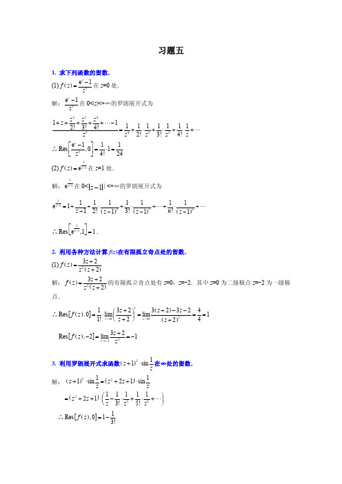
1 ∴ Res e z 1 ,1 1 .
2. 利用各种方法计算 f(z)在有限孤立奇点处的留数.
3z 2 (1) f z 2 z z 2 3z 2 解: f z 2 的有限孤立奇点处有 z=0,z=-2.其中 z=0 为二级极点 z=-2 为一级极 z z 2
1 1 2 解: z 1 sin z 2 2 z 1 sin z z 1 1 1 1 1 z 2 2 z 1 3 5 5! z z 3! z 1 ∴ Res f z , 0 1 3!
为在 c 内 tanπz 有 zk k
sin πz 由于 Res f z , zk cos πz
1 π
1 ∴ tan πzdz 2 πi Res f z , zk 2πi 2n 4ni c π k (2)
3 i 10
6. 计算下列积分.
(1)
π
0
cos m d 5 4 cos 1 π cos m d 2 π 5 4 cos
因被积函数为 θ 的偶函数,所以 I 令 I1
1 π sin m d 则有 2 π 5 4 cos
1 π eim d 2 π 5 4 cos
z 0
所以由留数定理.
AB
f z dz
BE
f z dz
EF
f z dz
C
FA
f z dz 2πi ln a
而
BE
f z dz
R
C
e x Ri ln a dx x Ri 2
EE352 Soldering Considerations for Exposed-Pad Packages (Rev 1, 05.2012)

Engineer-to-Engineer NoteEE-352Technical notes on using Analog Devices DSPs, processors and development toolsVisit our Web resources /ee-notes and /processors or e-mail processor.support@ or processor.tools.support@ for technical support.Soldering Considerations for Exposed-Pad PackagesContributed by Chirag Patel and Ramdas CharyRev 1 – May 17, 2012Copyright 2012, Analog Devices, Inc. All rights reserved. Analog Devices assumes no responsibility for customer product design or the use or application of customers’ products or for any infringements of patents or rights of others which may result from Analog Devices assistance. All trademarks and logos are property of IntroductionThis Engineer-to-Engineer Note is comprised of two main sections. The first section discusses general soldering guidelines for Analog Devices Inc. (ADI) DSP and processor boards, while the second section discusses specifically some commonly asked questions regarding Exposed pad (or EPAD) packages, requiring special considerations for soldering onto Printed Circuit Boards (PCBs). Special attention needs to be paid in order to ensure that electrical and thermal requirements are satisfied. This will ensureoptimum performance of the device.Determining the Temperature Profile for BoardsThe process of determining thetemperature profile for soldering components onto a custom board is determined by several factors, such as thickness and form factor of the board, the number and type of components, as well as the type of solder paste that is used (aero/mil or commercial/industrial). Solder paste vendors typically provide a reference document containing useful information, such as the recommended temperature profile for their paste. Based on this recommended profile for the type of solder paste used, it is advisable to populate a bare custom board with sufficient number of thermocouples, then pass it through the oven, and ensure that the appropriate temperature zones and times are reached.Figure 1 Recommended Heating Profile from Solder Paste vendorFigure 2 Heating Profile for typical ADI EZ-KitsAs a reference, Figure 1 and Figure 2 show the recommended temperature profile from the solder paste vendor, and the temperature profile followed in the oven for our EZ-KIT® boards. The attachment accompanying this EE-Note contains the datasheet from the solder paste vendor, as well as the temperature profile information used for most Analog Devices, Inc. EZ-KIT boards.arelight in density. customers boards toraw populated consideration. EZ-KIT boards anPackages Q1.Q2.keep them underPCBall and AND * noreliability. Q7.previousEPAD.Q8.problem?Lastly, technique.References[1] JESD No. 22-B102E Standard on Solderability , JEDEC Solid State Technology Association, 2007.[2] ADSP- 21483/21487/21488/21489 SHARC Embedded Processor Data Sheet. Rev A, April 2012. Analog Devices, Inc. [3] ADSP- BF592 Blackfin Embedded Processor Data Sheet. Rev A, August 2011. Analog Devices, Inc.Document History。
国科大高级电磁理论习题

第0章1. 作业题: 1.(1)求矢量22222324x y z A e x e x y e x y z的散度;(2)求A对中心在原点的一个单位立方体的积分;(3)求A对此立方体表面的积分,验证散度定理。
2. 求矢量22x y z A e x e x e y z沿xy 平面上的一个边长为2的正方形回路的线积分,此正方形的两边分别与x 轴和y 轴重合。
再求A对此回路所包围的曲面的面积分,验证斯托克斯定理。
3. 证明:(1)3r ;(2)0r; (3)()k r k 。
其中x y z r e x e y e z ,k 为一常矢量。
4. 利用直角坐标系,证明()+fG f G f G1. 有一内外半径分别为1r 和2r 的空心介质球,介质的电容率为 。
使介质内均匀带静止的自由电荷密度f ,求1.空间各点的电场;2.极化体电荷和极化面电荷分布。
2. 平行板电容器内有两层介质,他们的厚度分别为1l 和2l ,电容率为1 和2 ,今在两板接上电动势为E 的电池,求:1.电容器两板上的自由电荷面密度f ;2.介质分界面上的自由电荷面密度f ;3.若介质是漏电的,电导率为1 和2 ,当电流达到恒定时,上述两题的结果如何?3. 证明(1) 当两种绝缘介质的分界面上不带自由电荷时,电场线的曲折满足2211tan tan 其中1 和2 分别为两种介质的介电常数,1 和2 分别为界面两侧电场线与法线的夹角 (2)当两种导电介质内流有恒定电流时,分界面上电场线的曲折满足2211tan tan,其中1 和2 分别为两种介质的电导率。
4.试用边值关系证明:在绝缘介质与导体的分界面上,在静电情况下,导体外表面的电场线总是垂直于导体表面;在恒定电流的情况下导体表面的电场线总是平行于导体表面。
第一章1. 利用Fourier 变换,由时域形式的Maxwell 方程导出其频域形式。
解:付氏变换和付氏逆变换分别为:dt et f F tj)()(d e F t f tj)(21)( 麦氏方程:t D J HtB E0 BD对第一个方程进行付氏变换:),(),(), r H dt e t r H dt e t r H tj t j(左端),(),(),(),(),(),[ r D j r J dte t r D j r J dt e t t r D t r J t j tj(右端(时谐电磁场)),( r H ),(),( r D j r J同理可得:,,r B j r H0, r B,,r r D上面四式即为麦式方程的频域形式。
2EZ22D5中文资料

UPDATE : SEPTEMBER 9, 2000
元器件交易网
ELECTRICAL CHARACTERISTICS
Rating at = 25 ° C ambient temperature unless otherwise specified
TYPE
Nominal Zener Voltage VZ @ IZT IZT (V) (mA) 3.6 3.9 4.3 4.7 5.1 5.6 6.2 6.8 7.5 8.2 9.1 10 11 12 13 14 15 16 17 18 19 20 22 24 27 30 33 36 39 43 47 51 56 62 68 75 82 91 100 110 120 130 140 150 160 170 180 190 200 139 128 116 106 98.0 89.5 80.5 73.5 66.5 61.0 55.0 50.0 45.5 41.5 38.5 35.7 33.4 31.2 29.4 27.8 26.3 25.0 22.8 20.8 18.5 16.6 15.1 13.9 12.8 11.6 10.6 9.8 9.0 8.1 7.4 6.7 6.1 5.5 5.0 4.5 4.2 3.8 3.6 3.3 3.1 2.9 2.8 2.6 2.5
Maximum DC Zener Current IZM (mA) 504 468 434 386 356 324 292 266 242 220 200 182 166 152 138 130 122 114 107 100 95 90 82 76 68 60 55 50 47 43 39 36 32 29 27 24 22 20 18 17 15 14 13 12 11 11 10 10 9.0
3dmark05注册码

测完了报个分数:) [/quote]
咋么找到地,不会是专门干这地吧。;P强
只要你还在2005-12-7 12:45 PM
还有人要不??
查看完整版本: 求3dmark05注册码,在线等求助
Powered by Discuz! Archiver 4.0.0 © 2001-2005 Comsenz Technology Ltd
Processed in 0.013894 second(s), 2 queries
我这儿 01,03,05 的三个注册机全有。呵呵
mgy5972005-12-7 01:09 PM
[quote]原帖由 [i]hxh[/i] 于 2005-12-7 08:42 PM 发表
咋么找到地,不会是专门干这地吧。;P强 [/quote]
3DMark05 Build 1.0.0注册码:
L54A1-AJ24N-QZ8EK-9N5L5
HU8MJ-9H66E-3LL5Q-72B4Y
C5EQ3-4DW3M-600Y7-M4Q20
ZWKVR-WV3LM-VFPJY-SRE26
附上台式机实测分数(P4
3.0E,华硕P4P800SE,256*2DDR400,SATA80+160G,迪兰9600双128,长城300W)
laomeng_nb2005-12-7 06:27 PM
[quote]原帖由 [i]zhenhui[/i] 于 2005-12-7 09:29 PM 发表
3DMark05 Build 1.0.0注册码:
L54A1-AJ24N-QZ8EK-9N5L5
T3系列交流伺服驱动器说明书

¾ 产品特点
¾ T3a系列全密封设计,防护性好,抗干扰能力强 ¾ T3L系列小巧化设计,节省安装空间 ¾ T3/T3M/T3G控制接口采用机床行业主流定义方式,可实现无缝替换 ¾ 集速度控制、位置控制、转矩控制于一体 ¾ 可驱动各种类型的永磁同步伺服电机 ¾ 具有优异的低速转矩特性和业界领先的动态加减速性能
z 禁止将产品用于阳光直射,灰尘、盐分及金属粉末较多的场所。 z 禁止将产品用于有水、油及药品滴落的场所。
2. 配线
z 请将接地端子可靠接地,接地不良可能会造成触电或火灾。 z 请勿将220V驱动器电源接入380V电源,否则会造成设备损坏及触电或火灾。 z 请勿将U、V、W电机输出端子连接到三相电源,否则会造成人员伤亡或火灾。 z 必须将U、V、W电机输出端子和驱动器接线端子U、V、W一一对应连接,否则电机可
II
安全注意事项
在产品存放、安装、配线、运行、检查或维修前,用户必需熟悉并遵守以 下重要事项,以确保安全正确地使用本产品。
错误操作可能会引起危险并导致人身伤亡。 错误操作可能会引起危险,导致人身伤害,并可能使设备损坏。 严格禁止行为,否则会导致设备损坏或不能使用。
1. 使用场合
z 禁止将产品暴露在有水气、腐蚀性气体、可燃性气体的场合使用。否则会导致触电 或火灾。
能超速飞车造成设备损失与人员伤亡。 z 请紧固电源和电机输出端子,否则可能造成火灾。 z 配线请参考线材选择配线,否则可能造成火灾。
2EZ150中文资料

2EZ11 THRU 2EZ200GLASS PASSIVA TED JUNCTION SILICON ZENER DIODEVOLTAGE - 11 TO 200 Volts Power - 2.0 WattsFEA TURESl Low profile package l Built-in strain reliefl Glass passivated junction l Low inductancel Excellent clamping capabilityl Typical I D less than 1£g A above 11V l High temperature soldering : 260¢J /10 seconds at terminalsl Plastic package has Underwriters Laboratory Flammability Classification 94V-OMECHANICAL DATACase: JEDEC DO-15, Molded plastic over passivated junction Terminals: Solder plated, solderable per MIL-STD-750, method 2026Polarity: Color band denotes positive end (cathode)Standard Packaging: 52mm tape Weight: 0.015 ounce, 0.04 gramMAXIMUM RA TINGS AND ELECTRICAL CHARACTERISTICSRatings at 25¢J ambient temperature unless otherwise specified.SYMBOLVALUEUNITS Peak Pulse Power Dissipation (Note A)Derate above 75¢JP D 224Watts mW/¢J Peak forward Surge Current 8.3ms single half sine-wave superimposed on rated load(JEDEC Method) (Note B)I FSM 15Amps Operating Junction and Storage Temperature Range T J ,T STG -55 to +150¢JNOTES:A. Mounted on 5.0mm 2(.013mm thick) land areas.B. Measured on 8.3ms, single half sine-wave or equivalent square wave, duty cycle = 4 pulses per minute maximum.DO-152EZ11 THRU 2EZ200ELECTRICAL CHARACTERISTICS (T A =25¢J unless otherwise noted) V F =1.2 V max , I F =500 mA for all typesMaximum Zener Impedance (Note 3.)Leakage CurrentType No.(Note 1.)Nominal Zener Voltage Vz @ I ZT volts (Note 2.)T estcurrent I ZT mA Z ZT @ I ZT Ohms Z Zk @ I ZK Ohms I ZK mA I R £g A Max @V R Volts Maximum ZenerCurrent I ZM MadcSurge Current @ T A = 25¢J ir - mA (Note 4.)2EZ112EZ122EZ1311.012.013.045.541.538.5 4.04.55.07007007000.250.250.25 1.01.00.58.49.19.9166152138 1.821.661.542EZ142EZ152EZ162EZ172EZ1814.015.016.017.018.035.733.431.229.427.8 5.57.08.09.010.07007007007507500.250.250.250.250.250.50.50.50.50.510.611.412.213.013.7130122114107100 1.431.331.251.181.112EZ192EZ202EZ222EZ242EZ2719.020.022.024.027.026.325.022.820.818.511.011.012.013.018.07507507507507500.250.250.250.250.250.50.50.50.50.514.415.216.718.220.69590827668 1.051.000.910.830.742EZ302EZ332EZ362EZ392EZ4330.033.036.039.043.016.615.113.912.811.620.023.025.030.035.0100010001000100015000.250.250.250.250.250.50.50.50.50.522.525.127.429.732.760555047430.670.610.560.510.452EZ472EZ512EZ562EZ622EZ6847.051.056.062.068.010.69.89.08.17.440.048.055.060.075.0150015002000200020000.250.250.250.250.250.50.50.50.50.535.838.842.647.151.739363229270.420.390.360.320.292EZ752EZ822EZ912EZ1002EZ11075.082.091.0100.0110.0 6.76.15.55.04.590.0100.0125.0175.0250.0200030003000300040000.250.250.250.250.250.50.50.50.50.556.062.269.276.083.624222018170.270.240.220.200.182EZ1202EZ1302EZ1402EZ1502EZ160120.0130.0140.0150.0160.0 4.23.83.63.33.1325.0400.0500.0575.0650.0450050005500600065000.250.250.250.250.250.50.50.50.50.591.298.8106.4114.0121.615141312110.160.150.140.130.122EZ1702EZ1802EZ1902EZ200170.0180.0190.0200.02.92.82.62.5675.0725.0825.0900.070007000800080000.250.250.250.250.50.50.50.5130.4136.8144.8152.011101090.120.110.100.10NOTES:1. TOLERANCES - Suffix indicates 5% tolerance any other tolerance will be considered as a special device.2. ZENER VOLTAGE (Vz) MEASUREMENT - guarantees the zener voltage when measured at 40 ms ¡Ó10ms from the diode body, and an ambient temperature of 25¢J ( ¡Ï68¢J , -2¢J ).3.ZENER IMPEDANCE (Zz) DERIVATION - The zener impedance is derived from the 60 cycle ac voltage, which results when an ac current having an rms falue equal to 10% of the dc zener current (I ZT or I ZK ) is superimposed on I ZT or I ZK .4. SURGE CURRENT (Ir) NON-REPETITIVE - The rating listed in the electrical characteristics table is maximum peak, non-repetitive, reverse surge current of 1/2 square wave or equivalent sine wave pulse of 1/120 second duration superimposed on the test current, I ZT , per JEDEC standards, however, actual device capability is as described in Figure 3.0.00010.00020.00050.0010.0020.0050.010.020.050.10.20.512510Fig. 2-TYPICAL THERMAL RESPONSE L,P.W. PULSE WIDTH (ms)0.10.050.030.020.010.0050.0030.0020.0010.00050.00030.00020.0001 1251020501002005001KNOMINAL VZ (VOLTS)Fig. 3-MAXIMUM SURGE POWERFig. 4-TYPICAL REVERSE LEAKAGEVZ, ZENER VOLTAGE @IZT (VOLTS)VZ, ZENER VOLTAGE @IZT (VOLTS)Fig. 5-UNITS TO 12 VOLTS Fig. 6-UNITS 10 TO 200 VOLTSVZ, ZENER VOLTAGE (VOLTS)VZ, ZENER VOLTAGE (VOLTS)Fig. 7-VZ = 3.9 THRU 10 VOLTS Fig. 8-VZ = 12 THRU 82 VOLTSVZ, ZENER VOLTAGE (VOLTS)L, LEAD LENGTH TO HEAT SINK (INCH)Fig. 9-VZ = 100 THRU 200 VOLTS Fig. 10-TYPICAL THERMAL RESISTANCEAPPLICATION NOTE:Since the actual voltage available from a given zener diode is temperature dependent, it is necessary to determine junction temperature under any set of operating conditions in order to calculate its value. The following procedure is recommended:Lead Temperature, T L, should be determined from:TL = £c LA P D + T A£c LA is the lead-to-ambient thermal resistance (¢J/W) and P D is the power dissipation. The value for £c LA will vary and depends on the device mounting method.£c LA is generally 30-40¢J/W for the various chips and tie points in common use and for printed circuit board wiring.The temperature of the lead can also be measured using a thermocouple placed on the lead as close as possible to the tie point. The thermal mass connected to the tie point is normally large enough so that it will not significantly respond to heat surges generated in the diode as a result of pulsed operation once steady-state conditions are achieved. Using the measured value of T L, the junction temperature may be determined by:T J = T L + £G T JL£G T JL is the increase in junction temperature above the lead temperature and may be found from Figure 2 for a train of power pulses or from Figure 10 for dc power.£G T JL = £c LA P DFor worst-case design, using expected limits of Iz, limits of P D and the extremes of T J (£G T JL ) may be estimated. Changes in voltage, Vz, can then be found from:£G V = £c VZ £G T J£c VZ , the zener voltage temperature coefficient, is found from Figures 5 and 6.Under high power-pulse operation, the zener voltage will vary with time and may also be affected significantly be the zener resistance. For best regulation, keep current excursions as low as possible.Data of Figure 2 should not be used to compute surge capability. Surge limitations are given in Figure 3. They are lower than would be expected by considering only junction temperature, as current crowding effects cause temperatures to be extremely high in small spots resulting in device degradation should the limits of Figure 3 be exceeded.。
- 1、下载文档前请自行甄别文档内容的完整性,平台不提供额外的编辑、内容补充、找答案等附加服务。
- 2、"仅部分预览"的文档,不可在线预览部分如存在完整性等问题,可反馈申请退款(可完整预览的文档不适用该条件!)。
- 3、如文档侵犯您的权益,请联系客服反馈,我们会尽快为您处理(人工客服工作时间:9:00-18:30)。
2Watts Axial leaded Zener Diodes
Features
· Complete Voltage Range 3.6 to 200 Volts · High peak reverse power dissipation · High reliability · Low leakage current
WWW.SUNMATE.TW
Fig. 1 POWER TEMPERATURE DERATING CURVE PD, MAXIMUM DISSIPATION (WATTS) 2.5
L = 3/8" (9.5mm)
பைடு நூலகம்
2.0 1.5 1.0 0.5 0 0 25 50 75 100 125 150 175
TL, LEAD TEMPERATURE (° C)
Maximum Reverse Leakage Current IR @ VR (V) (µ A) 80 30 20 5.0 5.0 5.0 5.0 5.0 50 50 50 50 50 1.0 0.5 0.5 0.5 0.5 0.5 0.5 0.5 0.5 0.5 0.5 0.5 0.5 0.5 0.5 0.5 0.5 0.5 0.5 0.5 0.5 0.5 0.5 0.5 0.5 0.5 0.5 0.5 0.5 0.5 0.5 0.5 0.5 0.5 0.5 0.5 1.0 1.0 1.0 1.0 1.0 2.0 3.0 4.0 5.0 6.0 7.0 7.6 8.4 9.1 9.9 10.6 11.4 12.2 13.0 13.7 14.4 15.2 16.7 18.2 20.6 22.5 25.1 27.4 29.7 32.7 35.8 38.8 42.6 47.1 51.7 56.0 62.2 69.2 76.0 83.6 91.2 98.8 106.4 114.0 121.6 130.4 136.8 144.8 152.0
Symbol
PD VF RθJA TJ Ts
Value
2.0 1.2 60 - 55 to + 175 - 55 to + 175
Unit
Watts Volts K/W °C °C
Note : (1) TL = Lead temperature at 3/8 " (9.5mm) from body (2) Valid provided that leads are kept at ambient temperature at a distance of 10 mm from case.
2 of 2
D
C
DO-41 Dim A B C D Min 25.40 4.06 0.71 2.00 Max ¾ 5.21 0.864 2.72
All Dimensions in mm
Maximum Ratings and Electrical Characteristics
Single phase, half wave, 60Hz, resistive or inductive load.
1 of 2
ELECTRICAL CHARACTERISTICS
Rating at = 25 ° C ambient temperature unless otherwise specified
TYPE
Nominal Zener Voltage VZ @ IZT IZT (V) (mA) 3.6 3.9 4.3 4.7 5.1 5.6 6.2 6.8 7.5 8.2 9.1 10 11 12 13 14 15 16 17 18 19 20 22 24 27 30 33 36 39 43 47 51 56 62 68 75 82 91 100 110 120 130 140 150 160 170 180 190 200 139 128 116 106 98.0 89.5 80.5 73.5 66.5 61.0 55.0 50.0 45.5 41.5 38.5 35.7 33.4 31.2 29.4 27.8 26.3 25.0 22.8 20.8 18.5 16.6 15.1 13.9 12.8 11.6 10.6 9.8 9.0 8.1 7.4 6.7 6.1 5.5 5.0 4.5 4.2 3.8 3.6 3.3 3.1 2.9 2.8 2.6 2.5
Note : ( 1 ) Suffix " 5 " indicates ± 5.0% tolerance, suffix " 10 " indicates ± 10.0% tolerance. ( 2 ) " EZ " will be omitted in marking on the diode
WWW.SUNMATE.TW
ZZT @ IZT (Ω) 5.0 5.0 4.5 4.5 3.5 2.5 1.5 2.0 2.0 2.3 2.5 3.5 4.0 4.5 5.0 5.5 7.0 8.0 9.0 10 11 11 12 13 18 20 23 25 30 35 40 48 55 60 75 90 100 125 175 250 325 400 500 575 650 675 725 825 900
IZK (mA) 1.0 1.0 1.0 1.0 1.0 1.0 1.0 1.0 0.5 0.5 0.5 0.25 0.25 0.25 0.25 0.25 0.25 0.25 0.25 0.25 0.25 0.25 0.25 0.25 0.25 0.25 0.25 0.25 0.25 0.25 0.25 0.25 0.25 0.25 0.25 0.25 0.25 0.25 0.25 0.25 0.25 0.25 0.25 0.25 0.25 0.25 0.25 0.25 0.25
Maximum DC Zener Current IZM (mA) 504 468 434 386 356 324 292 266 242 220 200 182 166 152 138 130 122 114 107 100 95 90 82 76 68 60 55 50 47 43 39 36 32 29 27 24 22 20 18 17 15 14 13 12 11 11 10 10 9.0
2EZ3.6D5 2EZ3.9D5 2EZ4.3D5 2EZ4.7D5 2EZ5.1D5 2EZ5.6D5 2EZ6.2D5 2EZ6.8D5 2EZ7.5D5 2EZ8.2D5 2EZ9.1D5 2EZ10D5 2EZ11D5 2EZ12D5 2EZ13D5 2EZ14D5 2EZ15D5 2EZ16D5 2EZ17D5 2EZ18D5 2EZ19D5 2EZ20D5 2EZ22D5 2EZ24D5 2EZ27D5 2EZ30D5 2EZ33D5 2EZ36D5 2EZ39D5 2EZ43D5 2EZ47D5 2EZ51D5 2EZ56D5 2EZ62D5 2EZ68D5 2EZ75D5 2EZ82D5 2EZ91D5 2EZ100D5 2EZ110D5 2EZ120D5 2EZ130D5 2EZ140D5 2EZ150D5 2EZ160D5 2EZ170D5 2EZ180D5 2EZ190D5 2EZ200D5
A
B
A
Mechanical Data
· Case : DO-41 Molded plastic · Epoxy : UL94V-O rate flame retardant · Lead : Axial lead solderable per MIL-STD-202, method 208 guaranteed · Polarity : Color band denotes cathode end · Mounting position : Any · Weight : 0.339 gram
Maximum Zener Impedance ZZK @ IZK (Ω) 400 400 400 550 600 500 700 700 700 700 700 700 700 700 700 700 700 700 750 750 750 750 750 750 750 1000 1000 1000 1000 1500 1500 1500 2000 2000 2000 2000 3000 3000 3000 4000 4500 5000 5500 6000 6500 7000 7000 8000 8000
@ TA = 25°C unless otherwise specified
Rating
DC Power Dissipation at TL = 75 °C (Note1) Maximum Forward Voltage at IF = 200 mA Maximum Thermal Resistance Junction to Ambient Air (Note2) Junction Temperature Range Storage Temperature Range