TLWD1100B(T11)_en_datasheet_081226
上海高考填报志愿手册

atrust1000b2010 物理参数引言概述Atrust1000b2010是一款性能卓越的计算机设备,广泛应用于各行业的办公和生产环境。
为了更好地理解和使用这一设备,本文将深入探讨Atrust1000b2010的物理参数,包括其硬件规格、外部接口和独特设计等方面,为用户提供详细而全面的了解。
正文内容1. 外观和尺寸1.1 设备外观1.1.1 机箱材质:Atrust1000b2010采用何种材质制作机箱,以保证其坚固耐用,并有效散热。
1.1.2 设计风格:外观设计是否符合现代办公环境的审美标准,是否具备简洁、时尚的特点。
1.1.3 操作按钮和指示灯:机箱上是否设有方便操作的按钮,以及指示灯的种类和功能,提高设备的易用性。
1.2 尺寸和重量1.2.1 机箱尺寸:Atrust1000b2010的长度、宽度和高度是多少,以适应不同的场所布局。
1.2.2 设备重量:考虑到设备的搬运和安装,了解设备的重量对于用户具有实际意义。
1.2.3 安装方式:设备支持不同的安装方式,例如支持壁挂、桌面安放等,以满足各类用户的需求。
1.3 散热设计1.3.1 散热结构:Atrust1000b2010的散热结构采用何种设计,以确保设备在高负载工作时能够有效散热,保持稳定性能。
1.3.2 风扇噪音:了解设备风扇的噪音水平,以确保设备在工作时不会产生过多噪音,影响办公环境。
1.3.3 温度控制:设备是否配备温度传感器和自动调节装置,以保持设备在安全温度范围内运行。
2. 硬件规格2.1 处理器性能2.1.1 处理器型号:Atrust1000b2010采用何种型号的处理器,其主频和核心数是多少。
2.1.2 处理器架构:了解处理器的架构,以便更好地评估其性能和适用场景。
2.1.3 处理器升级:设备是否支持处理器的升级,以便满足未来对计算性能需求的提升。
2.2 存储设备2.2.1 内存容量:Atrust1000b2010支持的最大内存容量和内存类型是什么,以确保足够的内存支持多任务处理。
BR1100资料
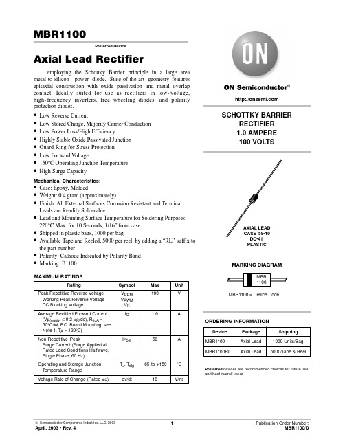
MBR1100Preferred DeviceAxial Lead Rectifier...employing the Schottky Barrier principle in a large area metal-to-silicon power diode. State-of-the-art geometry features epitaxial construction with oxide passivation and metal overlap contact. Ideally suited for use as rectifiers in low-voltage, high-frequency inverters, free wheeling diodes, and polarityprotection diodes.•Low Reverse Current•Low Stored Charge, Majority Carrier Conduction•Low Power Loss/High Efficiency•Highly Stable Oxide Passivated Junction•Guard-Ring for Stress Protection•Low Forward V oltage•150°C Operating Junction Temperature•High Surge CapacityMechanical Characteristics:•Case: Epoxy, Molded•Weight: 0.4 gram (approximately)•Finish: All External Surfaces Corrosion Resistant and Terminal Leads are Readily Solderable•Lead and Mounting Surface Temperature for Soldering Purposes: 220°C Max. for 10 Seconds, 1/16″ from case•Shipped in plastic bags, 1000 per bag•Available Tape and Reeled, 5000 per reel, by adding a “RL’’ suffix to the part number•Polarity: Cathode Indicated by Polarity Band•Marking: B1100MAXIMUM RATINGSPreferred devices are recommended choices for future use and best overall value.THERMAL CHARACTERISTICS (See Note 2)ELECTRICAL CHARACTERISTICS (T= 25°C unless otherwise noted)Figure 2. Typical Reverse Current {Figure 3. Current Derating (Mounting Method 3 per Note 1)Figure 4. Power Dissipation20102.05.01.0V R , REVERSE VOLTAGE (VOLTS)609000.20.040.020.011201600T A , AMBIENT TEMPERATURE (°C)4.03.02.01.00I F(AV), AVERAGE FORWARD CURRENT (AMPS)1.004.03.02.01.02.0140i F , I N S T A N T A N E O U S F O R W A R D C U R R E N T (A M P S )I I P F (A V ), A V E R A G E P O W E R D I S S I P A T I O N (W A T T S )0.50.20.1708010203040500.10.41.020********* 3.0 4.0 5.00.050.02100, R E V E R S E C U R R E N T ( A )R m 4.02.01020100402001 K400200180, A V E R A G E F O R W A R D C U R R E N T (A M P S )F (A V ){ The curves shown are typical for the highest voltagedevice in the voltage grouping. Typical reverse current for lower voltage selections can be estimated from these same curves if V R is sufficiently below rated V R .Figure 5. Typical Capacitance2040V R , REVERSE VOLTAGE (VOLTS)150504*********C , C A P A C I T A N C E (p F )50100601001070809070609080NOTE 1 — MOUNTING DATA:Data shown for thermal resistance junction-to-ambient (R q JA) for the mounting shown is to be used as a typical guideline values for preliminary engineering or in case the tie point temperature cannot be measured.Typical Values for Rin Still AirMounting Method 1P .C. Board with 1-1/2″ x 1-1/2″copper surface.Mounting Method 3P .C. Board with 1-1/2″ x 1-1/2″copper surface.VECTOR PIN MOUNTINGMounting Method 2NOTE 2 — THERMAL CIRCUIT MODEL:(For heat conduction through the leads)Use of the above model permits junction to lead thermal resistance for any mounting configuration to be found. For a given total lead length, lowest values occur when one side of the rectifier is brought as close as possible to the heat sink.Terms in the model signify:T A = Ambient Temperature T C = Case Temperature T L = Lead Temperature T J = Junction Temperature R q S = Thermal Resistance, Heat Sink to Ambient R q L = Thermal Resistance, Lead to Heat Sink R q J = Thermal Resistance, Junction to Case P D = Power Dissipation(Subscripts A and K refer to anode and cathode sides,respectively.) V alues for thermal resistance components are:R q L = 100°C/W/in typically and 120°C/W/in maximum.R θJ = 36°C/W typically and 46°C/W maximum.NOTE 3 — HIGH FREQUENCY OPERATION:Since current flow in a Schottky rectifier is the result of majority carrier conduction, it is not subject to junction diode forward and reverse recovery transients due to minority carrier injection and stored charge. Satisfactory circuit analysis work may be performed by using a model consisting of an ideal diode in parallel with a variable capacitance. (See Figure 5)Rectification efficiency measurements show that operation will be satisfactory up to several megahertz. For example, relative waveform rectification efficiency is approximately 70 percent at 2 MHz, e.g., the ratio of dc power to RMS power in the load is 0.28 at this frequency,whereas perfect rectification would yield 0.406 for sine wave inputs. However, in contrast to ordinary junction diodes, the loss in waveform efficiency is not indicative of power loss: it is simply a result of reverse current flow through the diode capacitance, which lowers the dc output voltage.PACKAGE DIMENSIONSCASE 59-10ISSUE SAXIAL LEAD, DO-41DIM MIN MAX MIN MAX MILLIMETERSINCHES A 4.10 5.200.1610.205B 2.00 2.700.0790.106D 0.710.860.0280.034F −−− 1.27−−−0.050K25.40−−−1.000−−−NOTES:1.DIMENSIONING AND TOLERANCING PER ANSI Y14.5M, 1982.2.CONTROLLING DIMENSION: INCH.3.59−04 OBSOLETE, NEW STANDARD 59−09.4.59−03 OBSOLETE, NEW STANDARD 59−10.5.ALL RULES AND NOTES ASSOCIATED WITH JEDEC DO−41 OUTLINE SHALL APPLY6.POLARITY DENOTED BY CATHODE BAND.7.LEAD DIAMETER NOT CONTROLLED WITHIN F DIMENSION.ON Semiconductor and are registered trademarks of Semiconductor Components Industries, LLC (SCILLC). SCILLC reserves the right to makechanges without further notice to any products herein. SCILLC makes no warranty, representation or guarantee regarding the suitability of its products for any particular purpose, nor does SCILLC assume any liability arising out of the application or use of any product or circuit, and specifically disclaims any and all liability, including without limitation special, consequential or incidental damages. “Typical” parameters which may be provided in SCILLC data sheets and/or specifications can and do vary in different applications and actual performance may vary over time. All operating parameters, including “Typicals” must be validated for each customer application by customer’s technical experts. SCILLC does not convey any license under its patent rights nor the rights of others.SCILLC products are not designed, intended, or authorized for use as components in systems intended for surgical implant into the body, or other applications intended to support or sustain life, or for any other application in which the failure of the SCILLC product could create a situation where personal injury or death may occur. Should Buyer purchase or use SCILLC products for any such unintended or unauthorized application, Buyer shall indemnify and hold SCILLC and its officers, employees, subsidiaries, affiliates, and distributors harmless against all claims, costs, damages, and expenses, and reasonable attorney fees arising out of, directly or indirectly, any claim of personal injury or death associated with such unintended or unauthorized use, even if such claim alleges that SCILLC was negligent regarding the design or manufacture of the part. SCILLC is an Equal Opportunity/Affirmative Action Employer.PUBLICATION ORDERING INFORMATIONJAPAN : ON Semiconductor, Japan Customer Focus Center 2-9-1 Kamimeguro, Meguro-ku, Tokyo, Japan 153-0051Phone : 81-3-5773-3850。
RTL8201数据手册

2. SYSTEM APPLICATIONS................................................................................................................1
3. FEATURES ..........................................................................................................................................2
5.1. LEAD (PB)-FREE PACKAGE AND VERSION IDENTIFICATION ...........................................................4
6. PIN DESCRIPTION............................................................................................................................5
ii
Track ID: JATR-1076-21 Rev. 1.3
RTL8201BL Datasheet
Table of Contents
1. INTRODUCTION ..........................................................1
Pin8: DVDD25-> PWFBIN
2. Add pull-high resistor for MDIO 3. Modify ResetB circuit to meet wake-on-LAN application Cosmetic layout changes
B1100B中文资料

1.0A HIGH VOLTAGE SCHOTTKY BARRIER RECTIFIERFeatures• Guard Ring Die Construction for Transient Protection• Ideally Suited for Automated Assembly• Low Power Loss, High Efficiency• Surge Overload Rating to 30A Peak• For Use in Low Voltage, High Frequency Inverters, Free Wheeling, and Polarity Protection Application• High Temperature Soldering: 260°C/10 Second at Terminal • Lead Free Finish/RoHS Compliant (Note 1)Mechanical Data• Case: SMA / SMB• Case Material: Molded Plastic. UL Flammability Classification Rating 94V-0• Moisture Sensitivity: Level 1 per J-STD-020D• Terminals: Lead Free Plating (Matte Tin Finish). Solderable per MIL-STD-202, Method 208• Polarity: Cathode Band or Cathode Notch• Marking Information: See Page 2• Ordering Information: See Page 2• Weight: SMA 0.064 grams (approximate)SMB 0.093 grams (approximate)Top View Bottom ViewMaximum Ratings@T A = 25°C unless otherwise specifiedSingle phase, half wave, 60Hz, resistive or inductive load.For capacitance load, derate current by 20%.Characteristic Symbol B170/B B180/B B190/B B1100/B UnitPeak Repetitive Reverse Voltage Working Peak Reverse Voltage DC Blocking Voltage V RRMV RWMV R70 80 90 100 VRMS Reverse Voltage V R(RMS)49 56 63 70 V Average Rectified Output Current @ T T = 125°C I O 1.0 A Non-Repetitive Peak Forward Surge Current 8.3msSingle Half Sine-Wave Superimposed on Rated LoadI FSM30 A Thermal CharacteristicsCharacteristic Symbol B170/B B180/B B190/B B1100/B Unit Typical Thermal Resistance Junction to Terminal (Note 2) RθJT25 °C/W Operating and Storage Temperature Range T J, T STG-65 to +150 °C Electrical Characteristics@T A = 25°C unless otherwise specifiedCharacteristic Symbol Min Typ Max Unit Test ConditionForward Voltage Drop V F- - 0.790.69VI F = 1.0A, T A = 25°CI F = 1.0A, T A = 100°CLeakage Current (Note 3) I R ----0.55.0mA@ Rated V R, T A = 25°C@ Rated V R, T A = 100°CTotal Capacitance C T- - 80 pF V R = 4V, f = 1MHz Notes: 1. EU Directive 2002/95/EC (RoHS). All applicable RoHS exemptions applied, see EU Directive 2002/95/EC Annex Notes.2. Valid provided that terminals are kept at ambient temperature.3. Short duration pulse test used to minimize self-heating effect.C , T O T A L C A P A C I T A N C E (p F )T V , DC REVERSE VOLTAGE (V)Fig. 2 Total Capacitance vs. Reverse Voltage RI ,I N S T A N T A N E O U S F O R W A R D C U R R E N T (A )F V , INSTANTANEOUS FORWARD VOLTAGE (V)Fig. 1 Typical Forward Characteristics F102030400I , 00.5255075100125150IA V E R A G E F O R W A R D C U R R E N T (A )F (A V ),T , TERMINAL TEMPERATURE (C)Fig. 3 Forward Current Derating CurveT °P E A K F O R W A R D S U R G E C U R R E N T (A )F S M NUMBER OF CYCLES AT 60 HzFig. 4 Max Non-Repetitive Peak Forward Surge CurrentOrdering Information (Note 4)Part NumberCase Packaging B1x-13-F SMA 5000/Tape & Reel B1xB-13-FSMB 3000/Tape & Reel*x = Device type, e.g. B180-13-F (SMA package); B1100B-13-F (SMB package).Notes: 4. For packaging details, go to our website at /datasheets/ap02007.pdf.Marking InformationXXX = Product type marking code, ex: B170 (SMA package) XXXX = Product type marking code, ex: B190B (SMB package) = Manufacturers’ code marking YWW = Date code markingY = Last digit of year ex: 2 for 2002 WW = Week code 01 to 52Package Outline DimensionsSuggested Pad LayoutIMPORTANT NOTICEDiodes Incorporated and its subsidiaries reserve the right to make modifications, enhancements, improvements, corrections or other changes without further notice to any product herein. Diodes Incorporated does not assume any liability arising out of the application or use of any product described herein; neither does it convey any license under its patent rights, nor the rights of others. The user of products in such applications shall assume all risks of such use and will agree to hold Diodes Incorporated and all the companies whose products are represented on our website, harmless against all damages.LIFE SUPPORTDiodes Incorporated products are not authorized for use as critical components in life support devices or systems without the expressed writtenapproval of the President of Diodes Incorporated.SMADim Min Max A 2.29 2.92 B 4.00 4.60 C 1.27 1.63 D 0.15 0.31 E 4.80 5.59 G 0.05 0.20 H 0.76 1.52 J 2.01 2.30 All Dimensions in mmSMBDim Min Max A 3.30 3.94 B 4.06 4.57 C 1.96 2.21 D 0.15 0.31 E 5.00 5.59 G 0.05 0.20 H 0.76 1.52 J 2.00 2.62 All Dimensions in mmSMADimensionsValue (in mm)Z 6.5 1.5 G 1.7X Y2.5C4.0SMBDimensionsValue (in mm)Z 6.7 G 1.8 X 2.3Y2.5 C4.3。
TLBA1100B(T11);中文规格书,Datasheet资料
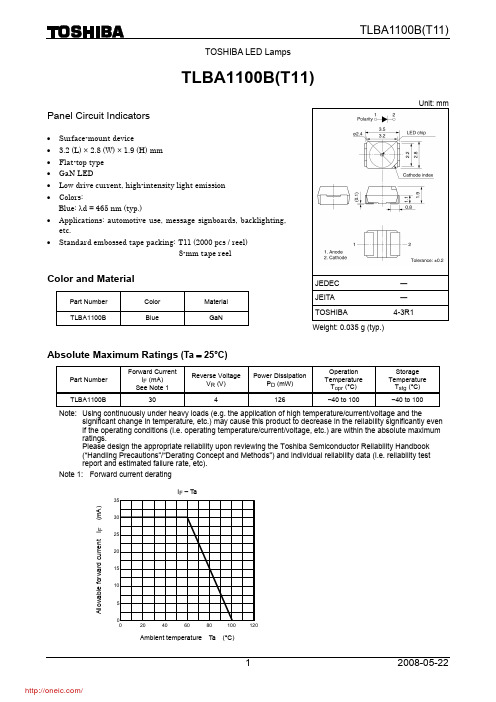
TOSHIBA LED LampsTLBA1100B(T11)Panel Circuit Indicators• Surface-mount device • 3.2 (L) × 2.8 (W) × 1.9 (H) mm • Flat-top type • GaN LED• Low drive current, high-intensity light emission • Colors:Blue: λd = 465 nm (typ.)• Applications: automotive use, message signboards, backlighting,etc. • Standard embossed tape packing: T11 (2000 pcs / reel) 8-mm tape reelColor and MaterialAbsolute Maximum Ratings (Ta = 25°C)Part NumberForward CurrentI F (mA) See Note 1Reverse VoltageV R (V)Power DissipationPD (mW)Operation Temperature T opr (°C)Storage Temperature T stg (°C) TLBA1100B 30 4 126 −40 to 100−40 to 100Note: Using continuously under heavy loads (e.g. the application of high temperature/current/voltage and thesignificant change in temperature, etc.) may cause this product to decrease in the reliability significantly even if the operating conditions (i.e. operating temperature/current/voltage, etc.) are within the absolute maximum ratings.Please design the appropriate reliability upon reviewing the Toshiba Semiconductor Reliability Handbook (“Handling Precautions”/“Derating Concept and Methods”) and individual reliability data (i.e. reliability test report and estimated failure rate, etc).Note 1: Forward current deratingUnit: mmJEDEC― JEITA―TOSHIBA 4-3R1 Weight: 0.035 g (typ.)Part NumberColorMaterialTLBA1100B BlueGaN0 20 40 60 80 100 120510 15 20 25 30 35Ambient temperature Ta (°C)I F – TaA l l o w a b l e f o r w a r d c u r r e n t I F (m A )Electrical Characteristics (Ta = 25°C)Forward Voltage V F Reverse CurrentI RPart NumberMin Typ. Max I F Max V RTLBA1100B 2.8 3.7 4.2 10 10 4Unit VmAμA VOptical Characteristics–1 (Ta = 25°C)Luminous Intensity I VPart NumberMin Typ. Max I FAvailable Iv rank (Note 2)TLBA1100B 4 7 20 10 JA / KA / LAUnit mcdmANote 2: The specification as following table is used for Iv classification of LEDs in Toshiba facility.Each reel includes the same rank LEDs. Let the delivery ratio of each rank be unquestioned.Iv rankRank symbol Min MaxJA 4.0 8.0KA 6.3 12.6LA 10.0 20.0Unit mcd mcdOptical Characteristics–2 (Ta = 25°C)Emission SpectrumPeak Emission Wavelength λp Δλ DominantWavelengthλdPart NumberMin Typ. Max Typ.Min Typ.MaxI FTLBA1100B ⎯428 ⎯60 462 465 472 10Unit nmnmnmmANote 3: CautionESD withstand voltage according to MIL STD 883D, Method 3015.7 : ≥1000VWhen handling this LED, take the following measures to prevent the LED from being damaged or otherwise adversely affected.1) Use a conductive tablemat and conductive floor mat, and ground the workbench and floor.2) Operators handling laser diodes must be grounded via a high resistance (about 1MΩ). A conductive strap isgood for this purpose.3) Ground all tools including soldering irons.This product is designed as a general display light source usage, and it has applied the measurement standard that matched with the sensitivity of human's eyes. Therefore, it is not intended for usage of functional application (ex. Light source for sensor, optical communication and etc) except general display light source.TLBA1100B−20 0 20 40 60 80 1000.20.40.60.811.21.4RelativeluminosityForward voltage V F (V)I F – V FForwardcurrentIF(mA)Forward current I F(mA)I V – I FLuminousintensityIV(mcd)Case temperature Tc (°C)I V– TcRelativeluminosityIVWavelength λ (nm)Relative luminosity - λTa = 25°CRadiation pattern30°0°60°90°90°30°60°1.00.80.60.40.280°70°50°40°20°10°70°80°50°40°20°10°(typ.)(typ.)(typ.)(typ.)(typ.)PackagingThis LED device is packed in an aluminum envelope with a silica gel and a moisture indicator to avoid moisture absorption. The optical characteristics of the devices may be affected by exposure to moisture in the air before soldering and they should therefore be stored under the following conditions:1. This moisture proof bag may be stored unopened within 12 months at the following conditions.Temperature: 5°C to 30°C Humidity: 90% (max)2. After opening the moisture proof bag, the devices should be assembled within 168 hours in an environment of5°C to 30°C/60% RH or below.3. If upon opening, the moisture indicator card shows humidity 30% or above (Color of indication changes topink) or the expiration date has passed, the devices should be baked in taping with reel. After baking, use the baked devices within 72 hours, but perform baking only once. Baking conditions: 60±5°C, for 12 to 24 hours.Expiration date: 12 months from sealing date, which is imprinted on the same side as this label affixed. 4. Repeated baking can cause the peeling strength of the taping to change, then leads to trouble in mounting.Furthermore, prevent the devices from being destructed against static electricity for baking of it.5. If the packing material of laminate would be broken, the hermeticity would deteriorate. Therefore, do notthrow or drop the packed devices.Mounting MethodSoldering• Reflow soldering (example)• The product is evaluated using above reflow soldering conditions. No additional test is performed exceed thecondition (i.e. the condition more than (*)MAX values) as a evaluation. Please perform reflow soldering under the above conditions.• Please perform the first reflow soldering with reference to the above temperature profile and within 168 h ofopening the package. • Second reflow solderingIn case of second reflow soldering should be performed within 168 h of the first reflow under the above conditions.Storage conditions before the second reflow soldering: 30°C, 60% RH (max) • Make any necessary soldering corrections manually.(only once at each soldering point) Soldering iron : 25 W Temperature : 300°C or less Time: within 3 s • If the product needs to be performed by other soldering method (ex. wave soldering), please contact Toshiba sales representative.Recommended soldering patternUnit: mmTime (s)P a c k a g e s u r f a c e t e m p e r a t u r e (°C )Temperature profile for Pb soldering (example)Time (s)P a c k a g e s u r f a c et e m p e r a t u r e (°C )Temperature profile for Pb-free soldering (example)CleaningWhen cleaning is required after soldering, Toshiba recommends the following cleaning solvents.It is confirmed that these solvents have no effect on semiconductor devices in our dipping test (under the recommended conditions). In selecting the one for your actual usage, please perform sufficient review on washing condition, using condition and etc.ASAHI CLEAN AK-225AES : (made by ASAHI GLASS) KAO CLEAN THROUGH 750H : (made by KAO)PINE ALPHA ST-100S: (made by ARAKAWA CHEMICAL)Precautions when MountingDo not apply force to the plastic part of the LED under high-temperature conditions. To avoid damaging the LED plastic, do not apply friction using a hard material.When installing the PCB in a product, ensure that the device does not come into contact with other cmponents.Tape Specifications1. Product number formatThe type of package used for shipment is denoted by a symbol suffix after the product number. The method of classification is as below. (this method, however does not apply to products whose electrical characteristics differ from standard Toshiba specifications) (1) Tape Type: T14 (4-mm pitch) (2) Example2. Tape dimensionsUnit: mmSymbol Dimension ToleranceSymbol Dimension ToleranceD 1.5 +0.1/−0 P 2 2.0 ±0.05E 1.75 ±0.1 W 8.0 ±0.3 P 0 4.0 ±0.1 P 4.0 ±0.1 t 0.3 ±0.05 A 0 2.9 ±0.1F 3.5 ±0.05 B 0 3.7 ±0.1 D 1 1.5 ±0.1 K 0 2.3 ±0.1TLBA1100B (T11)Tape typeToshiba product No.0Polarity3. Reel dimensionsUnit: mm4. Leader and trailer sections of tapeNote1: Empty trailer sectionNote2: Empty leader section5. Packing display(1) Packing quantityReel 2,000 pcs Carton 10,000 pcs(2) Packing form: Each reel is sealed in an aluminum pack with silica gel.6. Label format(1) Example: TLBA1100B (T11)P/N:TOSHIBATYPE TLBA1100BADDC(T11) Q’TY2,000 pcsLot Number Key code for TSB 32C 2000(RANK SYMBOL)Use under 5-30degC/6-%RH within 168hSEALED [[G]]/RoHS COMPATIBLE DIFFUSED IN ***** *Y380xxxxxxxxxxxxxxxxxx* ASSEMBLED IN *****(2) Label location• Reel• Carton• The aluminum package in which the reel is supplied also has the label attached to center of one side.RESTRICTIONS ON PRODUCT USE•Toshiba Corporation, and its subsidiaries and affiliates (collectively “TOSHIBA”), reserve the right to make changes to the information in this document, and related hardware, software and systems (collectively “Product”) without notice.•This document and any information herein may not be reproduced without prior written permission from TOSHIBA. Even with TOSHIBA’s written permission, reproduction is permissible only if reproduction is without alteration/omission.•Though TOSHIBA works continually to improve Product’s quality and reliability, Product can malfunction or fail. Customers are responsible for complying with safety standards and for providing adequate designs and safeguards for their hardware, software and systems which minimize risk and avoid situations in which a malfunction or failure of Product could cause loss of human life, bodily injury or damage to property, including data loss or corruption. Before creating and producing designs and using, customers must also refer to and comply with (a) the latest versions of all relevant TOSHIBA information, including without limitation, this document, the specifications, the data sheets and application notes for Product and the precautions and conditions set forth in the “TOSHIBA Semiconductor Reliability Handbook” and (b) the instructions for the application that Product will be used with or for. Customers are solely responsible for all aspects of their own product design or applications, including but not limited to (a) determining the appropriateness of the use of this Product in such design or applications; (b) evaluating and determining the applicability of any information contained in this document, or in charts, diagrams, programs, algorithms, sample application circuits, or any other referenced documents; and (c) validating all operating parameters for such designs and applications. TOSHIBA ASSUMES NO LIABILITY FOR CUSTOMERS’ PRODUCT DESIGN OR APPLICATIONS.•Product is intended for use in general electronics applications (e.g., computers, personal equipment, office equipment, measuring equipment, industrial robots and home electronics appliances) or for specific applications as expressly stated in this document.Product is neither intended nor warranted for use in equipment or systems that require extraordinarily high levels of quality and/or reliability and/or a malfunction or failure of which may cause loss of human life, bodily injury, serious property damage or serious public impact (“Unintended Use”). Unintended Use includes, without limitation, equipment used in nuclear facilities, equipment used in the aerospace industry, medical equipment, equipment used for automobiles, trains, ships and other transportation, traffic signaling equipment, equipment used to control combustions or explosions, safety devices, elevators and escalators, devices related to electric power, and equipment used in finance-related fields. Do not use Product for Unintended Use unless specifically permitted in this document.•Do not disassemble, analyze, reverse-engineer, alter, modify, translate or copy Product, whether in whole or in part.•Product shall not be used for or incorporated into any products or systems whose manufacture, use, or sale is prohibited under any applicable laws or regulations.•The information contained herein is presented only as guidance for Product use. No responsibility is assumed by TOSHIBA for any infringement of patents or any other intellectual property rights of third parties that may result from the use of Product. No license to any intellectual property right is granted by this document, whether express or implied, by estoppel or otherwise.•ABSENT A WRITTEN SIGNED AGREEMENT, EXCEPT AS PROVIDED IN THE RELEVANT TERMS AND CONDITIONS OF SALE FOR PRODUCT, AND TO THE MAXIMUM EXTENT ALLOWABLE BY LAW, TOSHIBA (1) ASSUMES NO LIABILITYWHATSOEVER, INCLUDING WITHOUT LIMITATION, INDIRECT, CONSEQUENTIAL, SPECIAL, OR INCIDENTAL DAMAGES OR LOSS, INCLUDING WITHOUT LIMITATION, LOSS OF PROFITS, LOSS OF OPPORTUNITIES, BUSINESS INTERRUPTION AND LOSS OF DATA, AND (2) DISCLAIMS ANY AND ALL EXPRESS OR IMPLIED WARRANTIES AND CONDITIONS RELATED TO SALE, USE OF PRODUCT, OR INFORMATION, INCLUDING WARRANTIES OR CONDITIONS OF MERCHANTABILITY, FITNESS FOR A PARTICULAR PURPOSE, ACCURACY OF INFORMATION, OR NONINFRINGEMENT.•Do not use or otherwise make available Product or related software or technology for any military purposes, including without limitation, for the design, development, use, stockpiling or manufacturing of nuclear, chemical, or biological weapons or missile technology products (mass destruction weapons). Product and related software and technology may be controlled under the Japanese Foreign Exchange and Foreign Trade Law and the U.S. Export Administration Regulations. Export and re-export of Product or related software or technology are strictly prohibited except in compliance with all applicable export laws and regulations. •Please contact your TOSHIBA sales representative for details as to environmental matters such as the RoHS compatibility of Product.Please use Product in compliance with all applicable laws and regulations that regulate the inclusion or use of controlled substances, including without limitation, the EU RoHS Directive. TOSHIBA assumes no liability for damages or losses occurring as a result of noncompliance with applicable laws and regulations.分销商库存信息: TOSHIBATLBA1100B(T11)。
ET310B用户手册

1序言尊敬的用户;感谢您选择本数字存储万用示波表,相信该产品创新的功能组合、人性化的设计会给您现场检测带来极大的方便。
使用前,请仔细阅读本手册内容,尤其“安全须知”部分。
阅读后请将此手册妥善保管,以备需要时随时查阅。
如果本手册不慎遗失,请登录 网站论坛下载。
ET521论坛是专业维修论坛,可以免费下载各种维修资料或提供技术支持;也是业内人士交流经验的平台。
参与论坛活动,将所获积分直接转换为电子货币,持币享有购买产品特殊优惠,还可以有偿转让。
知识产权本产品采用多项专有技术,购买或使用本机不代表所有者针对这些知识产权的任何权利转让。
未经本公司同意而仿制、应用全部或部分技术有可能触犯这些知识产权,属侵权行为。
知识产权包括但不限于专利权、商标权、出版物、网站内容等等。
• 本手册版权归珠海伊万电子科技有限公司所有。
• 本手册提供的信息取代以往出版的所有资料,如有变动只在本公司官方网站公告。
• 本公司的产品已获准及尚在审批的专利,受中华人民共和国专利法的保护。
• 本公司保留改变产品规格、价格及软件升级的权利。
• 本公司对产品手册及市场营销活动有最终解释权伊万科技注册的商标。
中国专利号:200720054112.0目 录安全须知 (5)仪表简介 (7)主要特点 (7)按键功能 (8)基本操作 (9)开机与关机 (9)自动关机 (9)背光的使用 (9)电池充电 (10)使用AC适配器供电 (10)仪表的复位 (11)示波表操作 (12)进入示波表模式 (12)示波表模式下的基本显示内容 (12)功能键与主选单 (13)输入信号耦合方式的选择 (13)时基控制 (14)水平位置调节 (14)垂直幅度控制 (15)2垂直位置调节 (15)触发控制 (16)触发电平调节 (16)关于触发模式 (17)扫描状态的提示信息 (17)单次扫描的触发操作 (18)游标测量读出功能 (19)波形的自动测量 (21)扫描参数的自动设置 (21)信号波形的保持 (22)上位机通讯软件(选件) (23)DSO模式下测量时与PC通信 (24)信号波形的存储与读出 (25)DSO数据库操作时与PC通信 (27)万用表操作 (28)进入万用表模式 (28)万用表模式下的基本显示内容 (28)测量功能切换 (29)手动/自动量程选择 (29)相对值测量模式 (30)3测量数据保持 (31)峰值保持(P-H)模式 (32)AC与DC电压测量 (33)分贝(dB)测量 (34)AC和DC电流(400mA,20A)测量 (35)频率计数与占空比测量 (36)电阻与电导测量 (37)二极管/通断测试 (39)电容测量 (39)温度/h FE /外接钳头/晶振测量(选件,下同) (40)DMM模式下测量时与PC通信 (44)测量数据的存储与读出 (44)DMM数据库操作时与PC通信 (46)系统设置及零点校正 (47)技术参数与仪表成套 (50)仪表特性与技术参数 (50)显示符号及图标 (53)仪表成套与选件 (55)日常维护与故障排除 (58)售后服务 (60)4本数字存储万用示波表的设计符合IEC1010-1安全规范,过压电测量第二类CAT III - 1000V,污染保护等级:1级。
WDGL-T1便携式报文及故障录波监测装置说明书
WDGL-T1 便携式报文及故障录波监测装置
用户手册
山东山大电力技术有限公司
目
录
Contents
1 技术特点............................................................................................................................................3 2 技术指标............................................................................................................................................5 3 技术原理............................................................................................................................................7
3.2 记录方式............................................................................................................................................................8 3.3 故障分析报告.....................................................................................................................................................9 3.4 输出方式.............................................................................................................................................................9
DS1100Z-50+;DS1100Z-100+;DS1100Z-500+;DS1100Z-250+;DS1100Z-60+;中文规格书,Datasheet资料

DC ELECTRICAL CHARACTERISTICS
(VCC = 5.0V ±5%, TA = -40°C to +85°C, unless otherwise noted.) PARAMETER SYMBOL CONDITIONS MIN Supply Voltage VCC 4.75 High-Level VIH 2.2 Input Voltage Low-Level VIL -0.3 Input Voltage Input-Leakage -1.0 II 0.0V ≤ VI ≤ VCC Current VCC = Max; Freq = Active Current ICC 1MHz High-Level VCC = Min; VOH = 4 IOH Output Current Low-Level VCC = Min; VOL = 0.5 12 IOL Output Current
+25°C 5V Input-to-Tap Delay Tolerance (Delays > 40ns) Power-Up Time Input Period tPLH, tPHL tPU Period 0°C to +70°C -40°C to +85°C -5 -8 -13 2(tWI) TYP MAX UNITS ns Table 1 Table 1 Table 1 Table 1 Table 1 Table 1 +2 +3 +4 +5 +8 +13 200 ns ns ns % % % μs ns NOTES 9 1, 3, 4, 7 1, 2, 3, 4, 7 1, 2, 3, 4, 7 1, 3, 4, 7 1, 2, 3, 4, 7 1, 2, 3, 4, 7 9
- 1、下载文档前请自行甄别文档内容的完整性,平台不提供额外的编辑、内容补充、找答案等附加服务。
- 2、"仅部分预览"的文档,不可在线预览部分如存在完整性等问题,可反馈申请退款(可完整预览的文档不适用该条件!)。
- 3、如文档侵犯您的权益,请联系客服反馈,我们会尽快为您处理(人工客服工作时间:9:00-18:30)。
TOSHIBA LED LampsTLWD1100B(T11)Panel Circuit Indicators• Surface-mount device• 3.2 (L) mm × 2.8 (W) mm × 1.9 (H) mm • LED chip and phosphor• Luminous intensity: I V = 180 mcd (typ.) @20 mA • Color: White• Chromaticity (typ.): Cx = 0.32, Cy = 0.31 •Topr / Tstg = -40 to 100°C• Reflow-solderable• Applications: automotive use, backlighting etc.• Standard embossed tape packing: T11 (2000pcs / reel) 8-mm tape reelColor and MaterialAbsolute Maximum Ratings (Ta = 25°C)Characteristics Symbol Rating UnitForward Current (Note 1) I F 30 mA Power Dissipation P D 120 mW Operating Temperature T opr −40 to 100 °C Storage TemperatureT stg−40 to 100°CNote: Using continuously under heavy loads (e.g. the application of high temperature/current/voltage and thesignificant change in temperature, etc.) may cause this product to decrease in the reliability significantly even if the operating conditions (i.e. operating temperature/current/voltage, etc.) are within the absolute maximum ratings.Please design the appropriate reliability upon reviewing the Toshiba Semiconductor Reliability Handbook (“Handling Precautions”/“Derating Concept and Methods”) and individual reliability data (i.e. reliability test report and estimated failure rate, etc).Note 1: Forward current deratingUnit: mmJEDEC ― JEITA―TOSHIBA 4-3R1 Weight: 0.035 g (typ.)Part NumberColorMaterial TLWD1100B WhiteInGaNI F – Ta0 20 40 60 80 100 120510 15 20 25 30 35 Ambient temperature Ta (°C)A l l o w a b l e f o r w a r d c u r r e n t I F (m A )洸子其科技是一家从事发光二极管产品研发、生产及销售公司,致力于为国内国际市场提供高品质,低成本的各类发光管。
主营产品有:SMD LED 0402、0603、0802、0805、1204、1206、3528、5050、3020、3014、2835、3535、335、020、正面发光及侧面发光,红、绿、蓝、白、黄、橙、粉红、紫、单色双色及三色等…主要应用:照明灯具、灯光亮化装饰工程、玩具礼品、背光显示、荧光验证防伪、手机、家电、MP3、手电筒、汽车、圣诞树、霓虹灯等…点击进入洸子其科技Electrical Characteristics (Ta = 25°C)Test condition Min Typ. Max Unit Characteristics SymbolForward Voltage V F I F= 20 mA 2.7 3.3 4.0 V Reverse Current I R V R= 4 V ⎯⎯ 10 μA Optical Characteristics (Ta = 25°C)Test condition Min Typ. Max Unit Characteristics SymbolC x I F= 20 mA (Note 2) ⎯ChromaticityC y I F= 20 mA (Note 2) ⎯Luminous Intensity (Note 3) I V I F= 20 mA 63 180 320mcd Note 2: The product is tested at the following chromaticity coordinate groups.I F=20 mA, Ta=25°Cconditions:TestTolerance: +/-0.01Note 3: I V rank classificationconditions:I F=20 mA, Ta=25°CTestLuminous intensity I VPart Numbermin typ max I FTLWD1100B(T11) 63 180 320QA⎯1256320⎯200RA100⎯320SA160mAUnit mcdThe specification on the above table is used for Iv classification of LEDs in Toshiba facility.Each reel includes the same rank LEDs. Let the delivery ratio of each rank be unquestioned.Note 4: CautionESD withstand voltage according to MIL STD 883D, Method 3015.7: ≥1000 VWhen handling this LED, take the following measures to prevent the LED from being damaged or otherwise adversely affected.1) Use a conductive tablemat and conductive floor mat, and ground the workbench and floor.2) Operators handling laser diodes must be grounded via a high resistance (about 1 MΩ). A conductive strap isgood for this purpose.3) Ground all tools including soldering irons.This product is designed as a general display light source usage, and it has applied the measurement standard that matched with the sensitivity of human's eyes. Therefore, it is not intended for usage of functional application (ex. Light source for sensor, optical communication and etc) except general display light source.TLWD1100B30.1110-40-20204060801000.00.20.40.60.81.03004005006007008000.290.30.310.320.330.34510152025303540Forward Voltage V F (V) I F – V FF o r w a r d C u r r e n t I F (m A )Forward Current I F (mA)I V /I V (20 mA) – I FL u m i n o u s i n t e n s i t y I V /I V (20 m A )Ta = 25°CRadiation pattern30°0°60° 90°90°30° 60° 1.00.8 0.60.4 0.2 0 80°70° 50° 40°20°10°70° 80° 50° 40° 20° 10°R e l a t i v e l u m i n o u s I n t e n s i t y I VC h r o m a t i c i t y C x , C yForward current I F (mA)Cx, Cy – I FCase Temperature Tc (°C)Relative I V – TcR e l a t i v e l u m i n o u s I n t e n s i t yWavelength λ (nm)Wavelength characteristic(typ.)(typ.)(typ.)(typ.)(typ.)(typ.)PackagingThese LED devices are packed in an aluminum envelope with a silica gel and a moisture indicator to avoidmoisture absorption. The optical characteristics of the devices may be affected by exposure to moisture in the air before soldering and they should therefore be stored under the following conditions:1. This moisture proof bag may be stored unopened within 12 months at the following conditions.Temperature: 5°C to 30°C Humidity: 90% (max)2. After opening the moisture proof bag, the devices should be assembled within 168 hours in an environment of5°C to 30°C / 60% RH or below.3. If upon opening, the moisture indicator card shows humidity 30% or above (Color of indication changes topink) or the expiration date has passed, the devices should be baked in taping with reel. After baking, use the baked devices within 72 hours, but perform baking only once. Baking conditions: 60 ± 5°C, for 12 to 24 hours.Expiration date: 12 months from sealing date, which is imprinted on the same side as this label affixed. 4. Repeated baking can cause the peeling strength of the taping to change, then leads to trouble in mounting.Furthermore, prevent the devices from being destructed against static electricity for baking of it.5. If the packing material of laminate would be broken, the hermeticity would deteriorate. Therefore, do notthrow or drop the packed devices.Mounting MethodSoldering• Reflow soldering• The product is evaluated using above reflow soldering conditions. No additional test is performed exceed thecondition (i.e. the condition more than (*)MAX values) as a evaluation. Please perform reflow soldering under the above conditions.• Please perform the first reflow soldering with reference to the above temperature profile and within 168 h ofopening the package. • Second reflow solderingIn case of second reflow soldering should be performed within 168 h of the first reflow under the above conditions.Storage conditions before the second reflow soldering: 30°C, 60% RH (max) • Make any necessary soldering corrections manually.(only once at each soldering point) Soldering iron: 25 WTemperature: 300°C or less Time:within 3 s • Do not perform flow soldering.Recommended soldering patternUnit: mmTime (s)P a c k a g e s u r f a c e t e m p e r a t u r e (°C )Temperature profile for Pb soldering (example)Time (s)P a c k a g e s u r f a c et e m p e r a t u r e (°C )Temperature profile for Pb-free soldering (example)CleaningWhen cleaning is required after soldering, Toshiba recommends the following cleaning solvents.It is confirmed that these solvents have no effect on semiconductor devices in our dipping test (under the recommended conditions). In selecting the one for your actual usage, please perform sufficient review on washing condition, using condition and etc.ASAHI CLEAN AK-225AES: (made by ASAHI GLASS)KAO CLEAN THROUGH 750H: (made by KAO)PINE ALPHA ST-100S:(made by ARAKAWA CHEMICAL)Precautions when Mounting(1) Do not apply force to the plastic part of the LED under high-temperature conditions.(2) To avoid damaging the LED plastic, do not apply friction using a hard material.(3) When installing the PCB in a product, ensure that the device does not come into contact with other cmponents. (4) For this product, silicone is used as the encapsulated material. Therefore the top surface of this product is soft. Please do not stress on the encapsulated part of LEDs to avoid affecting the reliability of the product. When using the mounting devices, please use the picking up nozzle that does not affect the silicone resin.Tape Specifications1. Product number formatThe type of package used for shipment is denoted by a symbol suffix after the product number. The method of classification is as below. (this method, however does not apply to products whose electrical characteristics differ from standard Toshiba specifications) (1) Tape Type: T11 (4-mm pitch) (2) Example2. Tape dimensionsUnit: mmSymbol Dimension ToleranceSymbol Dimension ToleranceD 1.5 +0.1/−0 P 2 2.0 ±0.05E 1.75 ±0.1 W 8.0 ±0.3 P 0 4.0 ±0.1 P 4.0 ±0.1 t 0.3 ±0.05 A 0 2.9 ±0.1F 3.5 ±0.05 B 0 3.7 ±0.1 D 1 1.5 ±0.1 K 0 2.3 ±0.1TLWD1100B (T11)Tape typeToshiba product No.3. Reel dimensionsUnit: mm4. Leader and trailer sections of tapeNote 1: Empty trailer sectionNote 2: Empty leader section5. Packing display(1) Packing quantityReel 2,000 pcs Carton 10,000 pcs(2) Packing form: Each reel is sealed in an aluminum pack with silica gel.6. Label format(1) Example: TLWD1100B (T11)P/N:TOSHIBATYPE TLWD1100BADDC(T11) Q’TY2,000 pcsLot Number Key code for TSB 32C 2000(RANK SYMBOL)Use under 5-30degC/6-%RH within 168hSEALED: [[G]]/RoHS COMPATIBLE DIFFUSED IN ***** *Y380xxxxxxxxxxxxxxxxxx* ASSEMBLED IN *****(2) Label location• Reel• Carton• The aluminum package in which the reel is supplied also has the label attached to center of one side.RESTRICTIONS ON PRODUCT USE20070701-EN GENERAL •The information contained herein is subject to change without notice.•TOSHIBA is continually working to improve the quality and reliability of its products. Nevertheless, semiconductor devices in general can malfunction or fail due to their inherent electrical sensitivity and vulnerability to physical stress. It is the responsibility of the buyer, when utilizing TOSHIBA products, to comply with the standards of safety in making a safe design for the entire system, and to avoid situations in which a malfunction or failure of such TOSHIBA products could cause loss of human life, bodily injury or damage to property.In developing your designs, please ensure that TOSHIBA products are used within specified operating ranges as set forth in the most recent TOSHIBA products specifications. Also, please keep in mind the precautions and conditions set forth in the “Handling Guide for Semiconductor Devices,” or “TOSHIBA Semiconductor Reliability Handbook” etc.• The TOSHIBA products listed in this document are intended for usage in general electronics applications (computer, personal equipment, office equipment, measuring equipment, industrial robotics, domestic appliances, etc.).These TOSHIBA products are neither intended nor warranted for usage in equipment that requires extraordinarily high quality and/or reliability or a malfunction or failure of which may cause loss of human life or bodily injury (“Unintended Usage”). Unintended Usage include atomic energy control instruments, airplane or spaceship instruments, transportation instruments, traffic signal instruments, combustion control instruments, medical instruments, all types of safety devices, etc.. Unintended Usage of TOSHIBA products listed in his document shall be made at the customer’s own risk.•The products described in this document shall not be used or embedded to any downstream products of which manufacture, use and/or sale are prohibited under any applicable laws and regulations.• The information contained herein is presented only as a guide for the applications of our products. No responsibility is assumed by TOSHIBA for any infringements of patents or other rights of the third parties which may result from its use. No license is granted by implication or otherwise under any patents or other rights of TOSHIBA or the third parties.• Please contact your sales representative for product-by-product details in this document regarding RoHS compatibility. Please use these products in this document in compliance with all applicable laws and regulations that regulate the inclusion or use of controlled substances. Toshiba assumes no liability for damage or losses occurring as a result of noncompliance with applicable laws and regulations.。