LM124ADR中文资料
LM258ADR中文资料

PACKAGING INFORMATIONOrderable Device Status(1)Package Type Package Drawing Pins Package Qty Eco Plan (2)Lead/Ball FinishMSL Peak Temp (3)5962-87710012A ACTIVE LCCC FK 201None POST-PLATE Level-NC-NC-NC 5962-8771001PA ACTIVE CDIP JG 81None A42SNPB Level-NC-NC-NC 5962-87710022A ACTIVE LCCC FK 201None POST-PLATE Level-NC-NC-NC 5962-8771002PA ACTIVE CDIP JG 81None A42SNPB Level-NC-NC-NC LM158AFKB ACTIVE LCCC FK 201None POST-PLATE Level-NC-NC-NCLM158AJG ACTIVE CDIP JG 81None A42SNPB Level-NC-NC-NC LM158AJGB ACTIVE CDIP JG 81None A42SNPB Level-NC-NC-NC LM158FKB ACTIVE LCCC FK 201None POST-PLATE Level-NC-NC-NCLM158JG ACTIVE CDIP JG 81None A42SNPB Level-NC-NC-NC LM158JGB ACTIVE CDIP JG 81None A42SNPB Level-NC-NC-NC LM258AD ACTIVE SOIC D 875Pb-Free (RoHS)CU NIPDAU Level-2-260C-1YEAR/Level-1-235C-UNLIM LM258ADGKR ACTIVE MSOP DGK 82500Green (RoHS &no Sb/Br)CU NIPDAU Level-2-260C-1YEAR LM258ADR ACTIVE SOIC D 82500Pb-Free (RoHS)CU NIPDAU Level-2-260C-1YEAR/Level-1-235C-UNLIM LM258AP ACTIVE PDIP P 850Pb-Free (RoHS)CU NIPDAU Level-NC-NC-NC LM258D ACTIVE SOIC D 875Pb-Free (RoHS)CU NIPDAU Level-2-260C-1YEAR/Level-1-235C-UNLIM LM258DGKR ACTIVE MSOP DGK 82500Green (RoHS &no Sb/Br)CU NIPDAU Level-2-260C-1YEAR LM258DR ACTIVE SOIC D 82500Green (RoHS &no Sb/Br)CU NIPDAU Level-1-260C-UNLIM LM258P ACTIVE PDIP P 850Pb-Free (RoHS)CU NIPDAU Level-NC-NC-NC LM2904AVQDR ACTIVE SOIC D 82500Pb-Free (RoHS)CU NIPDAU Level-2-250C-1YEAR/Level-1-235C-UNLIM LM2904AVQPWRACTIVE TSSOP PW 82000None CU NIPDAU Level-1-250C-UNLIM LM2904D ACTIVE SOIC D 875Pb-Free (RoHS)CU NIPDAU Level-2-260C-1YEAR/Level-1-235C-UNLIM LM2904DGKR ACTIVE MSOP DGK 82500Green (RoHS &no Sb/Br)CU NIPDAU Level-2-260C-1YEAR LM2904DR ACTIVE SOIC D 82500Green (RoHS &no Sb/Br)CU NIPDAU Level-1-260C-UNLIM LM2904P ACTIVE PDIP P 850Pb-Free (RoHS)CU NIPDAU Level-NC-NC-NC LM2904PSR ACTIVE SO PS 82000Pb-Free (RoHS)CU NIPDAU Level-2-260C-1YEAR/Level-1-235C-UNLIM LM2904PW ACTIVE TSSOP PW 8150Pb-Free (RoHS)CU NIPDAU Level-1-250C-UNLIM LM2904PWLE OBSOLETE TSSOP PW 8None Call TI Call TILM2904PWR ACTIVE TSSOP PW 82000Pb-Free (RoHS)CU NIPDAU Level-1-250C-UNLIM LM2904QD OBSOLETE SOIC D 8None Call TI Call TILM2904QDROBSOLETESOICD8Pb-Free (RoHS)CU NIPDAULevel-2-250C-1YEAR/Level-1-235C-UNLIMPACKAGE OPTION ADDENDUM4-Mar-2005Addendum-Page 1元器件交易网Orderable Device Status(1)PackageType PackageDrawingPins PackageQtyEco Plan(2)Lead/Ball Finish MSL Peak Temp(3)LM2904QP OBSOLETE PDIP P8None Call TI Call TILM2904VQDR ACTIVE SOIC D82500Pb-Free(RoHS)CU NIPDAU Level-2-250C-1YEAR/Level-1-235C-UNLIMLM2904VQPWR ACTIVE TSSOP PW82000None CU NIPDAU Level-1-250C-UNLIMLM358AD ACTIVE SOIC D875Pb-Free(RoHS)CU NIPDAU Level-2-260C-1YEAR/Level-1-235C-UNLIMLM358ADGKR ACTIVE MSOP DGK82500Green(RoHS&no Sb/Br)CU NIPDAU Level-2-260C-1YEARLM358ADR ACTIVE SOIC D82500Green(RoHS&no Sb/Br)CU NIPDAU Level-1-260C-UNLIMLM358AP ACTIVE PDIP P850Pb-Free(RoHS)CU NIPDAU Level-NC-NC-NCLM358APW ACTIVE TSSOP PW8150Pb-Free(RoHS)CU NIPDAU Level-1-250C-UNLIMLM358APWR ACTIVE TSSOP PW82000Pb-Free(RoHS)CU NIPDAU Level-1-250C-UNLIMLM358D ACTIVE SOIC D875Green(RoHS&no Sb/Br)CU NIPDAU Level-1-260C-UNLIMLM358DGKR ACTIVE MSOP DGK82500Green(RoHS&no Sb/Br)CU NIPDAU Level-2-260C-1YEARLM358DR ACTIVE SOIC D82500Green(RoHS&no Sb/Br)CU NIPDAU Level-1-260C-UNLIMLM358P ACTIVE PDIP P850Pb-Free(RoHS)CU NIPDAU Level-NC-NC-NCLM358PSLE OBSOLETE SO PS8None Call TI Call TILM358PSR ACTIVE SO PS82000Pb-Free(RoHS)CU NIPDAU Level-2-260C-1YEAR/Level-1-235C-UNLIMLM358PW ACTIVE TSSOP PW8150Pb-Free(RoHS)CU NIPDAU Level-1-250C-UNLIM LM358PWLE OBSOLETE TSSOP PW8None Call TI Call TILM358PWR ACTIVE TSSOP PW82000Pb-Free(RoHS)CU NIPDAU Level-1-250C-UNLIM(1)The marketing status values are defined as follows:ACTIVE:Product device recommended for new designs.LIFEBUY:TI has announced that the device will be discontinued,and a lifetime-buy period is in effect.NRND:Not recommended for new designs.Device is in production to support existing customers,but TI does not recommend using this part in a new design.PREVIEW:Device has been announced but is not in production.Samples may or may not be available.OBSOLETE:TI has discontinued the production of the device.(2)Eco Plan-May not be currently available-please check /productcontent for the latest availability information and additional product content details.None:Not yet available Lead(Pb-Free).Pb-Free(RoHS):TI's terms"Lead-Free"or"Pb-Free"mean semiconductor products that are compatible with the current RoHS requirements for all6substances,including the requirement that lead not exceed0.1%by weight in homogeneous materials.Where designed to be soldered at high temperatures,TI Pb-Free products are suitable for use in specified lead-free processes.Green(RoHS&no Sb/Br):TI defines"Green"to mean"Pb-Free"and in addition,uses package materials that do not contain halogens, including bromine(Br)or antimony(Sb)above0.1%of total product weight.(3)MSL,Peak Temp.--The Moisture Sensitivity Level rating according to the JEDECindustry standard classifications,and peak solder temperature.Important Information and Disclaimer:The information provided on this page represents TI's knowledge and belief as of the date that it isprovided.TI bases its knowledge and belief on information provided by third parties,and makes no representation or warranty as to the accuracy of such information.Efforts are underway to better integrate information from third parties.TI has taken and continues to take reasonable steps to provide representative and accurate information but may not have conducted destructive testing or chemical analysis on incoming materials and chemicals.TI and TI suppliers consider certain information to be proprietary,and thus CAS numbers and other limited information may not be available for release.In no event shall TI's liability arising out of such information exceed the total purchase price of the TI part(s)at issue in this document sold by TI to Customer on an annual basis.元器件交易网IMPORTANT NOTICETexas Instruments Incorporated and its subsidiaries (TI) reserve the right to make corrections, modifications,enhancements, improvements, and other changes to its products and services at any time and to discontinueany product or service without notice. Customers should obtain the latest relevant information before placingorders and should verify that such information is current and complete. All products are sold subject to TI’s termsand conditions of sale supplied at the time of order acknowledgment.TI warrants performance of its hardware products to the specifications applicable at the time of sale inaccordance with TI’s standard warranty. T esting and other quality control techniques are used to the extent TIdeems necessary to support this warranty. Except where mandated by government requirements, testing of allparameters of each product is not necessarily performed.TI assumes no liability for applications assistance or customer product design. Customers are responsible fortheir products and applications using TI components. T o minimize the risks associated with customer productsand applications, customers should provide adequate design and operating safeguards.TI does not warrant or represent that any license, either express or implied, is granted under any TI patent right,copyright, mask work right, or other TI intellectual property right relating to any combination, machine, or processin which TI products or services are used. Information published by TI regarding third-party products or servicesdoes not constitute a license from TI to use such products or services or a warranty or endorsement thereof.Use of such information may require a license from a third party under the patents or other intellectual propertyof the third party, or a license from TI under the patents or other intellectual property of TI.Reproduction of information in TI data books or data sheets is permissible only if reproduction is withoutalteration and is accompanied by all associated warranties, conditions, limitations, and notices. Reproductionof this information with alteration is an unfair and deceptive business practice. TI is not responsible or liable forsuch altered documentation.Resale of TI products or services with statements different from or beyond the parameters stated by TI for thatproduct or service voids all express and any implied warranties for the associated TI product or service andis an unfair and deceptive business practice. TI is not responsible or liable for any such statements.Following are URLs where you can obtain information on other Texas Instruments products and applicationsolutions:Products ApplicationsAmplifiers Audio /audioData Converters Automotive /automotiveDSP Broadband /broadbandInterface Digital Control /digitalcontrolLogic Military /militaryPower Mgmt Optical Networking /opticalnetworkMicrocontrollers Security /securityTelephony /telephonyVideo & Imaging /videoWireless /wirelessMailing Address:Texas InstrumentsPost Office Box 655303 Dallas, Texas 75265Copyright 2005, Texas Instruments Incorporated。
AMS124_05中文资料

Advanced AMS124 Monolithic MICROPOWER SHUNT VOLTAGE REFERENCE SystemsRoHS compliantFEATURES APPLICATIONS• Low Temperature Coefficient • Battery Powered Systems • Low Output Noise • Instrumentation • Operating Current 50µA to 4mA • Energy Management • Low Dynamic Impedance • Product Testing • Tight Output Voltage Tolerance • Precision Audio Components • Available in the sub-miniature SOT-23 Package • Data Acquisition SystemsGENERAL DESCRIPTIONThe AMS124 is a two-terminal micropower band-gap voltage reference diode featuring low dynamic impedance and good temperature coefficient, operating over a 50µA to 4mA current range. On-chip trimming is used to provide tight voltage tolerance. Since the AMS124 band-gap reference uses only transistors and resistors, low noise and good long term stability result. The wide dynamic operating range allows its use with widely varying supplies with excellent regulation. These voltage references can be used to make portable meters, regulators or general purpose analog circuitry.The AMS124 is operational in the full industrial temperature range of -40°C to 85°C and is available in small space saving SOT-23 package.ORDERING INFORMATION :MAX. PACKAGE TYPE OPERATING TEMPCO 3 LEAD SOT-23 TEMP. RANGE 50ppm/°C AMS124AM -40 to +85°C 100ppm/°C AMS124BM -40 to +85°CPIN CONNECTIONS3L SOT-23(M)*This pin must be left floating or connected to pin 2Top ViewAMS124ABSOLUTE MAXIMUM RATINGS (Note 1)Reverse Current 5mA Storage temperature -65°C to +150°C Forward Current10mA Internal Power Dissipation (P D ) Lead Temperature (25 sec) 265°CSOT-23 Package 0.28WThermal Resistance (θJA )SOT-23 Package 410°C/WELECTRICAL CHARACTERISTICSElectrical Characteristics at I R =500 µA and T A = +25°C unless otherwise specified. Parameter ConditionsAMS124A Min. Typ. Max.AMS124BMin. Typ. Max.UnitsOutput Voltage1.220 1.235 1.250 1.220 1.235 1.250VOutput Impedance0.6 2 0.6 2 ΩRMS Noise Voltage 10Hz ≤ f ≤ 10kHz 5 5 µVrms Temperature Coefficient T A = Full Range50100ppm/°CTurn-On Settling 0.1% of V OUT 15 15 µsec Operating Current(Note 3)0.0540.054mANote1: Absolute Maximum Ratings indicate limits beyond which damage to the device may occur. For guaranteed specifications and test conditions, see theElectrical Characteristics . The guaranteed specifications apply only for the test conditions listed.Note 2: Parameters identified with boldface type apply at temperature extremes. All other numbers apply at T A = T J = 25°C. Note 3: Optimum performance is obtained at currents below 500µA.TYPICAL APPLICATIONSShunt RegulatorPrecision 1µA to 1mA Current SourcesAMS124I OUT =1.2V/R2AMS124TYPICAL PERFORMANCE CHARACTERISTICS-0.5+0.50-0.1-0.2-0.3-0.4+0.4+0.3+0.2+0.1Temperature Drift for Different Average Temperature Coefficient V R C H A N G E (%)Reverse Characteristics and Minimum Operating Current FREQUENCY (Hz)FREQUENCY (Hz)Noise Voltage vs FrequencyAMS124 PACKAGE DIMENSIONS inches (millimeters) unless otherwise noted.3 LEAD SOT-23 PLASTIC PACKAGE (M)。
LM124AWRQMLV资料
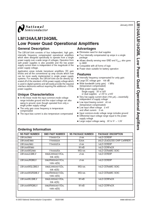
LM124A/LM124QMLLow Power Quad Operational AmplifiersGeneral DescriptionThe LM124/124A consists of four independent,high gain,internally frequency compensated operational amplifiers which were designed specifically to operate from a single power supply over a wide range of voltages.Operation from split power supplies is also possible and the low power supply current drain is independent of the magnitude of the power supply voltage.Application areas include transducer amplifiers,DC gain blocks and all the conventional op amp circuits which now can be more easily implemented in single power supply systems.For example,the LM124/124A can be directly op-erated off of the standard +5Vdc power supply voltage which is used in digital systems and will easily provide the required interface electronics without requiring the additional +15Vdc power supplies.Unique Characteristicsn In the linear mode the input common-mode voltage range includes ground and the output voltage can also swing to ground,even though operated from only a single power supply voltagen The unity gain cross frequency is temperature compensatedn The input bias current is also temperature compensatedAdvantagesn Eliminates need for dual suppliesn Four internally compensated op amps in a single packagen Allows directly sensing near GND and V OUT also goes to GNDn Compatible with all forms of logicn Power drain suitable for battery operationFeaturesn Internally frequency compensated for unity gain n Large DC voltage gain 100dBn Wide bandwidth (unity gain)1MHz (temperature compensated)n Wide power supply range:Single supply 3V to 32Vor dual supplies ±1.5V to ±16Vn Very low supply current drain (700µA)—essentially independent of supply voltage n Low input biasing current 45nA (temperature compensated)n Low input offset voltage 2mV and offset current:5nAn Input common-mode voltage range includes ground n Differential input voltage range equal to the power supply voltagen Large output voltage swing 0V to V +−1.5VOrdering InformationNS PART NUMBER SMD PART NUMBERNS PACKAGE NUMBERPACKAGE DISCRIPTION LM124J/8837704301CA J14A 14LD CERDIPLM124AE/88377043022A E20A 20LD LEADLESS CHIP CARRIER LM124AJ/8837704302CAJ14A 14LD CERDIP LM124AW/883W14B 14LD CERPACK LM124AWG/8837704302XA WG14A 14LD CERAMIC SOIC LM124AJLQMLV 5962L9950401VCA,50k rd(Si)J14A 14LD CERDIP LM124AJRQMLV 5962R9950401VCA,100k rd(Si)J14A 14LD CERDIP LM124AWGLQMLV 5962L9950401VZA,50k rd(Si)WG14A 14LD CERAMIC SOIC LM124AWGRQMLV 5962R9950401VZA,100k rd(Si)WG14A 14LD CERAMIC SOIC LM124AWLQMLV 5962L9950401VDA,50k rd(Si)W14B 14LD CERPACK LM124AWRQMLV5962R9950401VDA,100k rd(Si)W14B14LD CERPACKJanuary 2005LM124A/LM124QML Low Power Quad Operational Amplifiers©2005National Semiconductor Corporation Connection DiagramsLeadless Chip Carrier20108055See NS Package Number E20ADual-In-Line Package20108001Top ViewSee NS Package Number J14A20108033See NS Package Number W14B or WG14AL M 124A /L M 124Q M L 2LM124A/LM124QML Schematic Diagram(Each Amplifier)3Absolute Maximum Ratings (Note 1)If Military/Aerospace specified devices are required,please contact the National Semiconductor Sales Office/Distributors for availability and specifications.Supply Voltage,V +32Vdc or +16VdcDifferential Input Voltage 32VdcInput Voltage −0.3Vdc to +32VdcInput Current(V IN <−0.3Vdc)(Note 4)50mAPower Dissipation (Note 2)CERDIP 1260mW CERPACK 700mW LCC1350mW CERAMIC SOIC700mW Output Short-Circuit to GND (One Amplifier)(Note 3)V +≤15Vdc and T A =25˚C ContinuousOperating Temperature Range −55˚C ≤T A ≤+125˚CMaximum Junction Temperature 150˚CStorage Temperature Range−65˚C ≤T A ≤+150˚CLead Temperature (Soldering,10seconds)260˚C Thermal Resistance ThetaJA CERDIP (Still Air)103C/W (500LF/Min Air flow)51C/W CERPACK (Still Air)176C/W (500LF/Min Air flow)116C/W LCC (Still Air)91C/W (500LF/Min Air flow)66C/W CERAMIC SOIC (Still Air)176C/W (500LF/Min Air flow)116C/W ThetaJC CERDIP 19C/W CERPACK 18C/W LCC24C/W CERAMIC SOIC 18C/W Package Weight (Typical)CERDIP TBD CERPACK TBD LCCTBD CERAMIC SOIC 410mg ESD Tolerance (Note 5)250V Note 1:Absolute Maximum Ratings indicate limits beyond which damage to the device may occur.Operating Ratings indicate conditions for which the device is functional,but do not guarantee specific performance limits.For guaranteed specifications and test conditions,see the Electrical Characteristics.The guaranteed specifications apply only for the test conditions listed.Some performance characteristics may degrade when the device is not operated under the listed test conditions.Note 2:The maximum power dissipation must be derated at elevated temperatures and is dictated by Tjmax (maximum junction temperature),ThetaJA (package junction to ambient thermal resistance),and TA (ambient temperature).The maximum allowable power dissipation at any temperature is Pdmax =(Tjmax -TA)/ThetaJA or the number given in the Absolute Maximum Ratings,whichever is lower.Note 3:Short circuits from the output to V+can cause excessive heating and eventual destruction.When considering short circuits to ground,the maximum output current is approximately 40mA independent of the magnitude of V+.At values of supply voltage in excess of +15Vdc,continuous short-circuits can exceed the power dissipation ratings and cause eventual destruction.Destructive dissipation can result from simultaneous shorts on all amplifiers.Note 4:This input current will only exist when the voltage at any of the input leads is driven negative.It is due to the collector-base junction of the input PNP transistors becoming forward biased and thereby acting as input diode clamps.In addition to this diode action,there is also lateral NPN parasitic transistor action on the IC chip.This transistor action can cause the output voltages of the op amps to go to the V+voltage level (or to ground for a large overdrive)for the time duration that an input is driven negative.This is not destructive and normal output states will re-establish when the input voltage,which was negative,again returns to a value greater than -0.3Vdc (at 25C).Note 5:Human body model,1.5k Ωin series with 100pF.L M 124A /L M 124Q M L 4LM124A/LM124QML Quality Conformance InspectionMIL-STD-883,Method5005—Group ASubgroup Description Temp(˚C)1Static tests at+252Static tests at+1253Static tests at-554Dynamic tests at+255Dynamic tests at+1256Dynamic tests at-557Functional tests at+258A Functional tests at+1258B Functional tests at-559Switching tests at+2510Switching tests at+12511Switching tests at-555LM124A 883DC Electrical Characteristics(The following conditions apply to all the following parameters,unless otherwise specified.)All voltages referenced to device ground.SYMBOL PARAMETERCONDITIONSNOTESMINMAX UNIT SUB-GROUPS IccPower Supply Current V+=5V1.2mA 1,2,3V+=30V3.0mA 14.0mA 2,3IsinkOutput Sink CurrentV+=15V,Vout =200mV,+Vin =0mV,-Vin =+65mV 12uA 1V+=15V,Vout =2V,+Vin =0mV,-Vin =+65mV10mA 15mA 2,3Isource Output Source CurrentV+=15V,Vout =2V,+Vin =0mV,-Vin =-65mV -20mA 1-10mA 2,3Ios Short Circuit Current V+=5V,Vout =0V -60mA 1VioInput Offset VoltageV+=30V,Vcm =0V -22mV 1-44mV 2,3V+=30V,Vcm =28.5V -22mV 1V+=30V,Vcm =28V -44mV 2,3V+=5V,Vcm =0V-22mV 1-44mV 2,3CMRRCommon Mode Rejection Ratio V+=30V,Vin =0V to 28.5V 70dB 1±IibInput Bias Current V+=5V,Vcm =0V -5010nA 1-10010nA 2,3Iio Input Offset Current V+=5V,Vcm =0V -1010nA 1-3030nA 2,3PSRR Power Supply Rejection Ratio V+=5V to 30V,Vcm =0V 65dB 1Vcm Common Mode Voltage Range V+=30V(Note 6)28.5V 1(Note 6)28V 2,3Avs Large Signal Gain V+=15V,Rl =2K Ohms,Vo =1V to 11V(Note 7)50V/mV 4(Note 7)25V/mV 5,6VohOutput Voltage High V+=30V,Rl =2K Ohms 26V 4,5,6V+=30V,Rl =10K Ohms27V 4,5,6VolOutput Voltage LowV+=30V,Rl =10K Ohms 40mV 4,5,6V+=30V,Isink =1uA 40mV 4100mV 5,6V+=5V,Rl =10K Ohms20mV 4,5,6Channel Separation Amp to Amp Coupling1KHz,20KHz (Note 8)80dB4L M 124A /L M 124Q M L 6LM124883DC Electrical Characteristics(The following conditions apply to all the following parameters,unless otherwise specified.)All voltages referenced to device ground.SYMBOL PARAMETER CONDITIONS NOTES MIN MAX UNIT SUB-GROUPS Icc Power Supply Current V+=5V 1.2mA1,2,3V+=30V 3.0mA14.0mA2,3Isink Output Sink Current V+=15V,Vout=200mV,+Vin=0mV,-Vin=+65mV12uA1V+=15V,Vout=2V,+Vin=0mV,-Vin=+65mV 10mA15mA2,3Isource Output SourceCurrent V+=15V,Vout=2V,+Vin=0mV,-Vin=-65mV-20mA1-10mA2,3Ios Short Circuit Current V+=5V,Vout=0V-60mA1 Vio Input Offset Voltage V+=30V,Vcm=0V-55mV1-77mV2,3V+=30V,Vcm=28V-55mV1-77mV2,3V+=5V,Vcm=0V-55mV1-77mV2,3V+=30V,Vcm=28.5V-55mV1 CMRR Common ModeRejection RatioV+=30V,Vin=0V to28.5V70dB1 +Iib Input Bias Current V+=5V,Vcm=0V-15010nA1-30010nA2,3 Iio Input Offset Current V+=5V,Vcm=0V-3030nA1-100100nA2,3 PSRR Power SupplyRejection RatioV+=5V to30V,Vcm=0V65dB1Vcm Common ModeVoltage Range V+=30V(Note6)28.5V1(Note6)28V2,3Avs Large Signal Gain V+=15V,Rl=2K Ohms,Vo=1V to11V 50V/mV4 25V/mV5,6Voh Output Voltage High V+=30V,Rl=2K Ohms26V4,5,6V+=30V,Rl=10K Ohms27V4,5,6 Vol Output Voltage Low V+=30V,Rl=10K Ohms40mV4,5,6V+=30V,Isink=1uA40mV4100mV5,6V+=5V,Rl=10K Ohms20mV4,5,6Channel Separation (Amp to Amp Coupling)1KHz,20KHz(Note8)80dB4LM124A/LM124QML7LM124A RAD HARD DC Electrical Characteristics(Note 10)(The following conditions apply to all the following parameters,unless otherwise specified.)All voltages referenced to device ground.SYMBOL PARAMETER CONDITIONSNOTESMIN MAX UNIT SUB-GROUPS VioInput Offset VoltageVcc+=30V,Vcc-=Gnd,Vcm =-15V-22mV 1-44mV 2,3Vcc+=2V,Vcc-=-28V,Vcm =13V-22mV 1-44mV 2,3Vcc+=5V,Vcc-=Gnd,Vcm =-1.4V-22mV 1-44mV 2,3Vcc+=2.5V,Vcc-=-2.5,Vcm =1.1V-22mV 1-44mV 2,3IioInput Offset CurrentVcc+=30V,Vcc-=Gnd,Vcm =-15V-1010nA 1,2-3030nA 3Vcc+=2V,Vcc-=-28V,Vcm =13V-1010nA 1,2-3030nA 3Vcc+=5V,Vcc-=Gnd,Vcm =-1.4V-1010nA 1,2-3030nA 3Vcc+=2.5V,Vcc-=-2.5,Vcm =1.1V-1010nA 1,2-3030nA 3±IibInput Bias CurrentVcc+=30V,Vcc-=Gnd,Vcm =-15V-50+0.1nA 1,2-100+0.1nA 3Vcc+=2V,Vcc-=-28V,Vcm =13V-50+0.1nA 1,2-100+0.1nA 3Vcc+=5V,Vcc-=Gnd,Vcm =-1.4V-50+0.1nA 1,2-100+0.1nA 3Vcc+=2.5V,Vcc-=-2.5,Vcm =1.1V-50+0.1nA 1,2-100+0.1nA 3+PSRR Power Supply Rejection Ratio Vcc-=Gnd,Vcm =-1.4V,5V ≤Vcc ≤30V-100100uV/V 1,2,3CMRR Common Mode Rejection Ratio 76dB 1,2,3Ios+Output Short Circiut CurrentVcc+=30V,Vcc-=Gnd,Vo =25V-70mA 1,2,3IccPower Supply Current Vcc+=30V,Vcc-=Gnd3mA 1,24mA 3Delta Vio/Delta TInput Offset Voltage Temperature Sensitivity+25˚C ≤TA ≤+125˚C,+Vcc =5V,-Vcc =0V,Vcm =-1.4V(Note 9)-3030uV/˚C2-55˚C ≤TA ≤+25˚C,+Vcc =5V,-Vcc =0V,Vcm =-1.4V(Note 9)-3030uV/˚C 3Delta Iio/Delta TInput Offset Current Temperature Sensitivity+25˚C ≤TA ≤+125˚C,+Vcc =5V,-Vcc =0V,Vcm =-1.4V(Note 9)-400400pA/˚C2-55˚C ≤TA ≤+25˚C,+Vcc =5V,-Vcc =0V,Vcm =-1.4V(Note 9)-700700pA/˚C 3L M 124A /L M 124Q M L 8LM124A RAD HARD AC/DC Electrical Characteristics(Note10)(The following conditions apply to all the following parameters,unless otherwise specified.)All voltages referenced to device ground.SYMBOL PARAMETER CONDITIONS NOTES MIN MAX UNIT SUB-GROUPSVol Logical"0"OutputVoltage Vcc+=30V,Vcc-=Gnd,Rl=10K Ohms35mV4,5,6Vcc+=30V,Vcc-=Gnd,Iol=5mA1.5V4,5,6Vcc+=4.5V,Vcc-=Gnd,Iol=2uA0.4V4,5,6Voh Logical"1"OutputVoltage Vcc+=30V,Vcc-=Gnd,Ioh=-10mA27V4,5,6Vcc+=4.5V,Vcc-=Gnd,Ioh=-10mA2.4V4,5,6Avs+Voltage Gain Vcc+=30V,Vcc-=Gnd,1V≤Vo≤26V,Rl=10K Ohms50V/mV425V/mV5,6 Vcc+=30V,Vcc-=Gnd,5V≤Vo≤20V,Rl=2K Ohms50V/mV425V/mV5,6Avs Voltage Gain Vcc+=5V,Vcc-=Gnd,1V≤Vo≤2.5V,Rl=10K Ohms10V/mV4,5,6Vcc+=5V,Vcc-=Gnd,1V≤Vo≤2.5V,Rl=2K Ohms10V/mV4,5,6+Vop Maximum OutputVoltage Swing Vcc+=30V,Vcc-=Gnd,Vo=+30V,Rl=10K Ohms27V4,5,6Vcc+=30V,Vcc-=Gnd,Vo=+30V,Rl=2K Ohms26V4,5,6TR(tr)Transient Response:Rise TimeVcc+=30V,Vcc-=Gnd1uS7,8A,8BTR(os)Transient Response:OvershootVcc+=30V,Vcc-=Gnd50%7,8A,8B±Sr Slew Rate:Rise Vcc+=30V,Vcc-=Gnd0.1V/uS7,8A,8B Slew Rate:Fall Vcc+=30V,Vcc-=Gnd0.1V/uS7,8A,8BLM124A/LM124QML9LM124A RAD HARD —AC Electrical Characteristics(Note 10)(The following conditions apply to all the following parameters,unless otherwise specified.)AC:+Vcc =30V,-Vcc =0VSYMBOL PARAMETER CONDITIONSNOTESMINMAX UNIT SUB-GROUPS NI(BB)Noise Broadband +Vcc =15V,-Vcc =-15V,BW =10Hz to 5KHz 15uVrm s 7NI(PC)Noise Popcorn+Vcc =15V,-Vcc =-15V,Rs =20K Ohms,BW =10Hz to 5KHz 50uVpK7Cs Channel Separation +Vcc =30V,-Vcc =Gnd,Rl =2K Ohms80dB 7Rl =2K Ohms,Vin =1V and 16V,A to B 80dB 7Rl =2K Ohms,Vin =1V and 16V,A to C 80dB 7Rl =2K Ohms,Vin =1V and 16V,A to D 80dB 7Rl =2K Ohms,Vin =1V and 16V,B to A 80dB 7Rl =2K Ohms,Vin =1V and 16V,B to C 80dB 7Rl =2K Ohms,Vin =1V and 16V,B to D 80dB 7Rl =2K Ohms,Vin =1V and 16V,C to A 80dB 7Rl =2K Ohms,Vin =1V and 16V,C to B 80dB 7Rl =2K Ohms,Vin =1V and 16V,C to D 80dB 7Rl =2K Ohms,Vin =1V and 16V,D to A 80dB 7Rl =2K Ohms,Vin =1V and 16V,D to B 80dB 7Rl =2K Ohms,Vin =1V and 16V,D to C80dB7L M 124A /L M 124Q M L 10LM124A/LM124QML LM124A RAD HARD—DC Drift Values(Note10)(The following conditions apply to all the following parameters,unless otherwise specified.)DC:"Delta calculationsperformedon QMLV devices at group B,subgroup5only"SYMBOL PARAMETER CONDITIONS NOTES MIN MAX UNIT SUB-GROUPSVio Input Offset Voltage Vcc+=30V,Vcc-=Gnd,-0.50.5mV1Vcm=-15V±Iib Input Bias Current Vcc+=30V,Vcc-=Gnd,-1010nA1Vcm=-15VElectrical Characteristics—POST RADIATION LIMITS+25˚C(Note10)(The following conditions apply to all the following parameters,unless otherwise specified.)All voltages referenced to device ground.SYMBOL PARAMETER CONDITIONS NOTES MIN MAX UNIT SUB-GROUPS(Note10)-2.5 2.5mV1Vio Input Offset Voltage Vcc+=30V,Vcc-=Gnd,Vcm=-15VVcc+=2V,Vcc-=-28V,(Note10)-2.5 2.5mV1Vcm=13V(Note10)-2.5 2.5mV1Vcc+=5V,Vcc-=GND,Vcm=-1.4V(Note10)-2.5 2.5mV1Vcc+=2.5V,Vcc-=-2.5,Vcm=1.1VIio Input Offset Current Vcc+=30V,Vcc-=GND,(Note10)-1515nA1Vcm=-15V(Note10)-1515nA1Vcc+=2V,Vcc-=-28V,Vcm=13VVcc+=5V,Vcc-=GND,(Note10)-1515nA1Vcm=-1.4V(Note10)-1515nA1Vcc+=2.5V,Vcc-=-2.5V,Vcm=1.1V±Iib Input Bias Current Vcc+=30V,Vcc-=GND,(Note10)-75+0.1nA1Vcm=-15V(Note10)-75+0.1nA1Vcc+=2V,Vcc-=-28V,Vcm=13VVcc+=5V,Vcc-=GND,(Note10)-75+0.1nA1Vcm=-1.4V(Note10)-75+0.1nA1Vcc+=2.5V,Vcc-=-2.5V,Vcm=1.1VAvs+Voltage Gain Vcc+=30V,Vcc-=GND,(Note10)40V/mV41V≤Vo≤26V,Rl=10K Ohms(Note10)40V/mV4Vcc+=30V,Vcc-=GND,5V≤Vo≤20V,Rl=2K OhmsNote6:Guaranteed by Vio tests.Note7:Datalog reading in K=V/mVNote8:Guaranteed,not testedNote9:Calculated parametersNote10:Pre and post irradiation limits are identical to those listed under AC and DC electrical characteristics except as listed in the Post Radiation Limits Table.These parts may be dose rate sensitive in a space environment and demonstrate enhanced low dose rate effect.Radiation end point limits for the noted parameters are guaranteed only for the conditions as specified in MIL-STD-883,Method1019Typical Performance CharacteristicsInput Voltage RangeInput Current2010803420108035Supply Current Voltage Gain2010803620108037Open Loop FrequencyResponse Common Mode RejectionRatio2010803820108039L M 124A /L M 124Q M LTypical Performance Characteristics(Continued)Voltage Follower PulseResponseVoltage Follower PulseResponse(Small Signal) 2010804020108041Large Signal FrequencyResponseOutput CharacteristicsCurrent Sourcing 2010804220108043Output CharacteristicsCurrent Sinking Current Limiting2010804420108045LM124A/LM124QMLApplication HintsThe LM124series are op amps which operate with only a single power supply voltage,have true-differential inputs,and remain in the linear mode with an input common-mode voltage of 0V DC .These amplifiers operate over a wide range of power supply voltage with little change in performance characteristics.At 25˚C amplifier operation is possible down to a minimum supply voltage of 2.3V DC .The pinouts of the package have been designed to simplify PC board layouts.Inverting inputs are adjacent to outputs for all of the amplifiers and the outputs have also been placed at the corners of the package (pins 1,7,8,and 14).Precautions should be taken to insure that the power supply for the integrated circuit never becomes reversed in polarity or that the unit is not inadvertently installed backwards in a test socket as an unlimited current surge through the result-ing forward diode within the IC could cause fusing of the internal conductors and result in a destroyed unit.Large differential input voltages can be easily accommo-dated and,as input differential voltage protection diodes are not needed,no large input currents result from large differ-ential input voltages.The differential input voltage may be larger than V +without damaging the device.Protection should be provided to prevent the input voltages from going negative more than −0.3V DC (at 25˚C).An input clamp diode with a resistor to the IC input terminal can be used.To reduce the power supply drain,the amplifiers have a class A output stage for small signal levels which converts to class B in a large signal mode.This allows the amplifiers to both source and sink large output currents.Therefore both NPN and PNP external current boost transistors can be used to extend the power capability of the basic amplifiers.The output voltage needs to raise approximately 1diode drop above ground to bias the on-chip vertical PNP transistor for output current sinking applications.For ac applications,where the load is capacitively coupled to the output of the amplifier,a resistor should be used,from the output of the amplifier to ground to increase the class A bias current and prevent crossover distortion.Where the load is directly coupled,as in dc applications,there is no crossover distortion.Capacitive loads which are applied directly to the output of the amplifier reduce the loop stability margin.Values of 50pF can be accommodated using the worst-case non-inverting unity gain rge closed loop gains or resistive isolation should be used if larger load capacitance must be driven by the amplifier.The bias network of the LM124establishes a drain current which is independent of the magnitude of the power supply voltage over the range of from 3V DC to 30V DC .Output short circuits either to ground or to the positive power supply should be of short time duration.Units can be de-stroyed,not as a result of the short circuit current causing metal fusing,but rather due to the large increase in IC chip dissipation which will cause eventual failure due to exces-sive junction temperatures.Putting direct short-circuits on more than one amplifier at a time will increase the total IC power dissipation to destructive levels,if not properly pro-tected with external dissipation limiting resistors in series with the output leads of the amplifiers.The larger value of output source current which is available at 25˚C provides a larger output current capability at elevated temperatures (see typical performance characteristics)than a standard IC op amp.The circuits presented in the section on typical applications emphasize operation on only a single power supply voltage.If complementary power supplies are available,all of the standard op amp circuits can be used.In general,introduc-ing a pseudo-ground (a bias voltage reference of V +/2)will allow operation above and below this value in single power supply systems.Many application circuits are shown which take advantage of the wide input common-mode voltage range which includes ground.In most cases,input biasing is not required and input voltages which range to ground can easily be accommodated.L M 124A /L M 124Q M LTypical Single-Supply Applications(V+=5.0V DC)Non-Inverting DC Gain(0V Input=0V Output)20108005 *R not needed due to temperature independent I INDC Summing Amplifier(V IN’S≥0V DC and V O≥V DC)Power Amplifier20108006 Where:V0=V1+V2−V3−V4(V1+V2)≥(V3+V4)to keep V O>0V DC20108007V0=0V DC for V IN=0V DCA V=10LM124A/LM124QMLTypical Single-Supply Applications (V +=5.0V DC )(Continued)LED Driver“BI-QUAD”RC Active Bandpass Filter2010800820108009f o =1kHz Q =50A V =100(40dB)Fixed Current Sources Lamp Driver2010801020108011L M 124A /L M 124Q M LTypical Single-Supply Applications(V+=5.0V DC)(Continued)Current Monitor20108012*(Increase R1for I L small)Driving TTL20108013Voltage Follower20108014Pulse Generator20108015Squarewave Oscillator20108016Pulse Generator20108017LM124A/LM124QMLTypical Single-Supply Applications (V +=5.0V DC )(Continued)High Compliance Current Sink20108018I O =1amp/volt V IN (Increase R E for I o small)Low Drift Peak Detector20108019L M 124A /L M 124Q M LTypical Single-Supply Applications (V +=5.0V DC )(Continued)Comparator with HysteresisGround Referencing a Differential Input Signal2010802020108021V O =V RVoltage Controlled Oscillator Circuit20108022*Wide control voltage range:0V DC ≤V C ≤2(V +−1.5V DC )Photo Voltaic-Cell Amplifier20108023LM124A/LM124QMLTypical Single-Supply Applications (V +=5.0V DC )(Continued)AC Coupled Inverting Amplifier20108024AC Coupled Non-Inverting Amplifier20108025L M 124A /L M 124Q M LTypical Single-Supply Applications (V +=5.0V DC )(Continued)DC Coupled Low-Pass RC Active Filter20108026f O =1kHz Q =1A V =2High Input Z,DC Differential Amplifier20108027LM124A/LM124QML21Typical Single-Supply Applications (V +=5.0V DC )(Continued)High Input Z Adjustable-Gain DC Instrumentation Amplifier20108028Using Symmetrical Amplifiers to Reduce Input Current (General Concept)20108029Bridge Current Amplifier20108030L M 124A /L M 124Q M L 22LM124A/LM124QMLTypical Single-Supply Applications(V+=5.0V)(Continued)DCBandpass Active Filter Array20108031f O=1kHzQ=2523Revision History SectionDateReleased RevisionSectionOriginator Changes9–2–04ANew Release,Corporate formatR.Malone3MDS data sheets converted into one Corp.data sheet format.MNLM124-X,Rev.1A2,MNLM124A-X,Rev.1A3and MRLM124A-X-RH,Rev.5A0.MDS data sheets will be archived.01/27/05BConnection Diagrams,Quality Conformance Inspection Section,and Physical Dimensions drawingsR.MaloneAdded E package Connection Diagram.Changed verbiage under Quality Conformance Title,and UpdatedRevisions for the Marketing Drawings.L M 124A /L M 124Q M L 24Physical Dimensionsinches (millimeters)unless otherwise notedSAMPLE TEXT Ceramic Dual-In-Line Package (J)NS Package Number J14ASAMPLE TEXT 20Pin Leadless Chip Carrier,Type C (E)NS Package Number E20ALM124A/LM124QML25Physical Dimensionsinches (millimeters)unless otherwise noted (Continued)SAMPLE TEXT Ceramic Flatpak PackageNS Package Number W14BSAMPLE TEXT 14-Pin Ceramic Package (WG)NS Package Number WG14AL M 124A /L M 124Q M L 26NotesNational does not assume any responsibility for use of any circuitry described,no circuit patent licenses are implied and National reserves the right at any time without notice to change said circuitry and specifications.For the most current product information visit us at .LIFE SUPPORT POLICYNATIONAL’S PRODUCTS ARE NOT AUTHORIZED FOR USE AS CRITICAL COMPONENTS IN LIFE SUPPORT DEVICES OR SYSTEMS WITHOUT THE EXPRESS WRITTEN APPROVAL OF THE PRESIDENT AND GENERAL COUNSEL OF NATIONAL SEMICONDUCTOR CORPORATION.As used herein:1.Life support devices or systems are devices or systemswhich,(a)are intended for surgical implant into the body,or(b)support or sustain life,and whose failure to perform whenproperly used in accordance with instructions for use provided in the labeling,can be reasonably expected to result in a significant injury to the user.2.A critical component is any component of a life supportdevice or system whose failure to perform can be reasonably expected to cause the failure of the life support device or system,or to affect its safety or effectiveness.BANNED SUBSTANCE COMPLIANCENational Semiconductor certifies that the products and packing materials meet the provisions of the Customer Products Stewardship Specification(CSP-9-111C2)and the Banned Substances and Materials of Interest Specification(CSP-9-111S2)and contain no‘‘Banned Substances’’as defined in CSP-9-111S2.National Semiconductor Americas CustomerSupport CenterEmail:new.feedback@ Tel:1-800-272-9959National SemiconductorEurope Customer Support CenterFax:+49(0)180-5308586Email:europe.support@Deutsch Tel:+49(0)6995086208English Tel:+44(0)8702402171Français Tel:+33(0)141918790National SemiconductorAsia Pacific CustomerSupport CenterEmail:ap.support@National SemiconductorJapan Customer Support CenterFax:81-3-5639-7507Email:jpn.feedback@Tel:81-3-5639-7560 LM124A/LM124QML Low Power Quad Operational Amplifiers。
LM224中文资料_数据手册_参数
Parameter Supply Voltage
Input Voltage
Differential Input Voltage - (*)
Power Dissipation
N Suffix D Suffix
Output Short-circuit Duration - (note 1)
Supply Voltage Rejection (VCCT+am=b5=V+t2o53o0CV)
Ratio
(RS
≤
10kΩ)
Tmin. ≤ Tamb ≤ Tmax.
Supply Current, all Amp, no load
Tamb = +25oC
VCC = +5V
VCC = +30V
Tmin. ≤ Tamb ≤ Tmax.
(VCCTa=mb+5=V+,2R5LoC= 2kΩ)
Tmin. ≤ Tamb ≤ Tmax.
RL = 2kΩ RL = 10kΩ
Low Level Tamb =
Output +25oC
Voltage
(RL
=
10kΩ)
Tmin. ≤ Tamb ≤ Tmax.
Slew Rate VCC = 15V, VI = 0.5 to 3V, RL = 2kΩ, CL = 100pF, unity gain)
Input Offset Current Drift
Channel Separation (note 5) 1kHz ≤ f ≤ 20kHz
MHz
1.3 %
0.015
nV
40
LM324DR PDF资料
LM124, LM124A, LM224K, LM224KA,LM124, LM124A, LM224, LM224A, LM324,LM124, LM124A,LM124, LM124A, LM224, LM224A, LM324,LM124, LM124A,LM124, LM124A, LM224, LM224A, LM324,LM124, LM124A,LM124, LM124A, LM224, LM224A, LM324, LM324A, LM2902, LM2902V,LM124, LM124A,IMPORTANT NOTICETexas Instruments Incorporated and its subsidiaries (TI) reserve the right to make corrections, modifications, enhancements, improvements, and other changes to its products and services at any time and to discontinue any product or service without notice. Customers should obtain the latest relevant information before placing orders and should verify that such information is current and complete. All products are sold subject to TI’s terms and conditions of sale supplied at the time of order acknowledgment.TI warrants performance of its hardware products to the specifications applicable at the time of sale in accordance with TI’s standard warranty. T esting and other quality control techniques are used to the extent TI deems necessary to support this warranty. Except where mandated by government requirements, testing of all parameters of each product is not necessarily performed.TI assumes no liability for applications assistance or customer product design. Customers are responsible for their products and applications using TI components. T o minimize the risks associated with customer products and applications, customers should provide adequate design and operating safeguards.TI does not warrant or represent that any license, either express or implied, is granted under any TI patent right, copyright, mask work right, or other TI intellectual property right relating to any combination, machine, or process in which TI products or services are used. Information published by TI regarding third-party products or services does not constitute a license from TI to use such products or services or a warranty or endorsement thereof. Use of such information may require a license from a third party under the patents or other intellectual property of the third party, or a license from TI under the patents or other intellectual property of TI.Reproduction of information in TI data books or data sheets is permissible only if reproduction is without alteration and is accompanied by all associated warranties, conditions, limitations, and notices. Reproduction of this information with alteration is an unfair and deceptive business practice. TI is not responsible or liable for such altered documentation.Resale of TI products or services with statements different from or beyond the parameters stated by TI for that product or service voids all express and any implied warranties for the associated TI product or service and is an unfair and deceptive business practice. TI is not responsible or liable for any such statements. Following are URLs where you can obtain information on other Texas Instruments products and application solutions:Products ApplicationsAmplifiers Audio /audioData Converters Automotive /automotiveDSP Broadband /broadbandInterface Digital Control /digitalcontrolLogic Military /militaryPower Mgmt Optical Networking /opticalnetwork Microcontrollers Security /securityTelephony /telephonyVideo & Imaging /videoWireless /wirelessMailing Address:Texas InstrumentsPost Office Box 655303 Dallas, Texas 75265Copyright 2005, Texas Instruments Incorporated。
LM124DRG4资料
PACKAGING INFORMATIONOrderableDevice Status (1)Package Type Package DrawingPins Package Qty Eco Plan (2)Lead/Ball Finish MSL Peak Temp (3)5962-7704301VCAACTIVE CDIP J 141TBD A42SNPB N /A for Pkg Type 77043012A ACTIVE LCCC FK 201TBD POST-PLATE N /A for Pkg Type7704301CA ACTIVE CDIP J 141TBD A42SNPB N /A for Pkg Type 7704301DA ACTIVE CFP W 141TBD A42SNPB N /A for Pkg Type 77043022A ACTIVE LCCC FK 201TBD POST-PLATE N /A for Pkg Type7704302CA ACTIVE CDIP J 141TBD A42SNPB N /A for Pkg Type JM38510/11005BCAACTIVE CDIP J 141TBD A42SNPB N /A for Pkg Type LM124ADR OBSOLETE SOIC D 14TBD Call TI Call TILM124AFKB ACTIVE LCCC FK 201TBD POST-PLATE N /A for Pkg TypeLM124AJ ACTIVE CDIP J 141TBD A42SNPB N /A for Pkg Type LM124AJB ACTIVE CDIP J 141TBD A42SNPB N /A for Pkg Type LM124D ACTIVE SOIC D 1450TBD CU NIPDAU Level-3-245C-168HR LM124DG4ACTIVE SOIC D 1450Green (RoHS &no Sb/Br)CU NIPDAU Level-1-260C-UNLIM LM124DR ACTIVE SOIC D 142500TBDCU NIPDAU Level-3-245C-168HR LM124DRG4ACTIVE SOIC D 142500Green (RoHS &no Sb/Br)CU NIPDAULevel-1-260C-UNLIMLM124FKB ACTIVE LCCC FK 201TBD POST-PLATE N /A for Pkg Type LM124J ACTIVE CDIP J 141TBD A42SNPB N /A for Pkg Type LM124JB ACTIVE CDIP J 141TBD A42SNPB N /A for Pkg Type LM124N OBSOLETE PDIP N 14TBD Call TI Call TILM124W ACTIVE CFP W 141TBD A42SNPB N /A for Pkg Type LM124WB ACTIVE CFP W 141TBD A42SNPB N /A for Pkg Type LM224AD ACTIVE SOIC D 1450Green (RoHS &no Sb/Br)CU NIPDAU Level-1-260C-UNLIM LM224ADE4ACTIVE SOIC D 1450Green (RoHS &no Sb/Br)CU NIPDAU Level-1-260C-UNLIM LM224ADG4ACTIVE SOIC D 1450Green (RoHS &no Sb/Br)CU NIPDAU Level-1-260C-UNLIM LM224ADR ACTIVE SOIC D 142500Green (RoHS &no Sb/Br)CU NIPDAU Level-1-260C-UNLIM LM224ADRE4ACTIVE SOIC D 142500Green (RoHS &no Sb/Br)CU NIPDAU Level-1-260C-UNLIM LM224ADRG4ACTIVE SOIC D 142500Green (RoHS &no Sb/Br)CU NIPDAU Level-1-260C-UNLIM LM224AN ACTIVE PDIP N 1425Pb-Free (RoHS)CU NIPDAU N /A for Pkg Type LM224ANE4ACTIVE PDIP N 1425Pb-Free (RoHS)CU NIPDAU N /A for Pkg Type LM224D ACTIVE SOIC D 1450Green (RoHS &no Sb/Br)CU NIPDAU Level-1-260C-UNLIM LM224DE4ACTIVE SOIC D 1450Green (RoHS &no Sb/Br)CU NIPDAU Level-1-260C-UNLIM LM224DG4ACTIVE SOIC D 1450Green (RoHS &no Sb/Br)CU NIPDAU Level-1-260C-UNLIM LM224DRACTIVESOICD142500Green (RoHS &CU NIPDAULevel-1-260C-UNLIMPACKAGE OPTION ADDENDUM9-Oct-2007Addendum-Page 1OrderableDeviceStatus (1)Package Type Package DrawingPins Package QtyEco Plan (2)Lead/Ball FinishMSL Peak Temp (3)no Sb/Br)LM224DRE4ACTIVE SOIC D 142500Green (RoHS &no Sb/Br)CU NIPDAU Level-1-260C-UNLIM LM224DRG4ACTIVE SOIC D 142500Green (RoHS &no Sb/Br)CU NIPDAU Level-1-260C-UNLIM LM224KAD ACTIVE SOIC D 1450Green (RoHS &no Sb/Br)CU NIPDAU Level-1-260C-UNLIM LM224KADE4ACTIVE SOIC D 1450Green (RoHS &no Sb/Br)CU NIPDAU Level-1-260C-UNLIM LM224KADG4ACTIVE SOIC D 1450Green (RoHS &no Sb/Br)CU NIPDAU Level-1-260C-UNLIM LM224KADR ACTIVE SOIC D 142500Green (RoHS &no Sb/Br)CU NIPDAU Level-1-260C-UNLIM LM224KADRE4ACTIVE SOIC D 142500Green (RoHS &no Sb/Br)CU NIPDAU Level-1-260C-UNLIM LM224KADRG4ACTIVE SOIC D 142500Green (RoHS &no Sb/Br)CU NIPDAU Level-1-260C-UNLIM LM224KAN ACTIVE PDIP N 1425Pb-Free (RoHS)CU NIPDAU N /A for Pkg Type LM224KANE4ACTIVE PDIP N 1425Pb-Free (RoHS)CU NIPDAU N /A for Pkg Type LM224KD ACTIVE SOIC D 1450Green (RoHS &no Sb/Br)CU NIPDAU Level-1-260C-UNLIM LM224KDE4ACTIVE SOIC D 1450Green (RoHS &no Sb/Br)CU NIPDAU Level-1-260C-UNLIM LM224KDG4ACTIVE SOIC D 1450Green (RoHS &no Sb/Br)CU NIPDAU Level-1-260C-UNLIM LM224KDR ACTIVE SOIC D 142500Green (RoHS &no Sb/Br)CU NIPDAU Level-1-260C-UNLIM LM224KDRE4ACTIVE SOIC D 142500Green (RoHS &no Sb/Br)CU NIPDAU Level-1-260C-UNLIM LM224KDRG4ACTIVE SOIC D 142500Green (RoHS &no Sb/Br)CU NIPDAU Level-1-260C-UNLIM LM224KN ACTIVE PDIP N 1425Pb-Free (RoHS)CU NIPDAU N /A for Pkg Type LM224KNE4ACTIVE PDIP N 1425Pb-Free (RoHS)CU NIPDAU N /A for Pkg Type LM224N ACTIVE PDIP N 1425Pb-Free (RoHS)CU NIPDAU N /A for Pkg Type LM224NE4ACTIVE PDIP N 1425Pb-Free (RoHS)CU NIPDAU N /A for Pkg Type LM2902D ACTIVE SOIC D 1450Green (RoHS &no Sb/Br)CU NIPDAU Level-1-260C-UNLIM LM2902DE4ACTIVE SOIC D 1450Green (RoHS &no Sb/Br)CU NIPDAU Level-1-260C-UNLIM LM2902DG4ACTIVE SOIC D 1450Green (RoHS &no Sb/Br)CU NIPDAU Level-1-260C-UNLIM LM2902DR ACTIVE SOIC D 142500Green (RoHS &no Sb/Br)CU NIPDAU Level-1-260C-UNLIM LM2902DRE4ACTIVESOICD142500Green (RoHS &no Sb/Br)CU NIPDAULevel-1-260C-UNLIM9-Oct-2007OrderableDevice Status (1)Package Type Package DrawingPins Package Qty Eco Plan (2)Lead/Ball Finish MSL Peak Temp (3)LM2902DRG4ACTIVE SOIC D 142500Green (RoHS &no Sb/Br)CU NIPDAU Level-1-260C-UNLIM LM2902KAVQDR NRND SOIC D 142500Pb-Free (RoHS)CU NIPDAU Level-2-250C-1YEAR/Level-1-235C-UNLIM LM2902KAVQDRG4ACTIVE SOIC D 142500Green (RoHS &no Sb/Br)CU NIPDAU Level-1-260C-UNLIM LM2902KAVQPWR ACTIVE TSSOP PW 142000TBDCU NIPDAU Level-1-250C-UNLIM LM2902KAVQPWRG4ACTIVE TSSOP PW 142000Green (RoHS &no Sb/Br)CU NIPDAU Level-1-260C-UNLIM LM2902KD ACTIVE SOIC D 1450Green (RoHS &no Sb/Br)CU NIPDAU Level-1-260C-UNLIM LM2902KDB ACTIVE SSOP DB 1480Green (RoHS &no Sb/Br)CU NIPDAU Level-1-260C-UNLIM LM2902KDBE4ACTIVE SSOP DB 1480Green (RoHS &no Sb/Br)CU NIPDAU Level-1-260C-UNLIM LM2902KDBG4ACTIVE SSOP DB 1480Green (RoHS &no Sb/Br)CU NIPDAU Level-1-260C-UNLIM LM2902KDBR ACTIVE SSOP DB 142000Green (RoHS &no Sb/Br)CU NIPDAU Level-1-260C-UNLIM LM2902KDBRE4ACTIVE SSOP DB 142000Green (RoHS &no Sb/Br)CU NIPDAU Level-1-260C-UNLIM LM2902KDBRG4ACTIVE SSOP DB 142000Green (RoHS &no Sb/Br)CU NIPDAU Level-1-260C-UNLIM LM2902KDE4ACTIVE SOIC D 1450Green (RoHS &no Sb/Br)CU NIPDAU Level-1-260C-UNLIM LM2902KDG4ACTIVE SOIC D 1450Green (RoHS &no Sb/Br)CU NIPDAU Level-1-260C-UNLIM LM2902KDR ACTIVE SOIC D 142500Green (RoHS &no Sb/Br)CU NIPDAU Level-1-260C-UNLIM LM2902KDRE4ACTIVE SOIC D 142500Green (RoHS &no Sb/Br)CU NIPDAU Level-1-260C-UNLIM LM2902KDRG4ACTIVE SOIC D 142500Green (RoHS &no Sb/Br)CU NIPDAU Level-1-260C-UNLIM LM2902KN ACTIVE PDIP N 1425Pb-Free (RoHS)CU NIPDAU N /A for Pkg Type LM2902KNE4ACTIVE PDIP N 1425Pb-Free (RoHS)CU NIPDAU N /A for Pkg Type LM2902KNSR ACTIVE SO NS 142000Green (RoHS &no Sb/Br)CU NIPDAU Level-1-260C-UNLIM LM2902KNSRE4ACTIVE SO NS 142000Green (RoHS &no Sb/Br)CU NIPDAU Level-1-260C-UNLIM LM2902KNSRG4ACTIVE SO NS 142000Green (RoHS &no Sb/Br)CU NIPDAU Level-1-260C-UNLIM LM2902KPW ACTIVE TSSOP PW 1490Green (RoHS &no Sb/Br)CU NIPDAU Level-1-260C-UNLIM LM2902KPWE4ACTIVE TSSOP PW 1490Green (RoHS &no Sb/Br)CU NIPDAU Level-1-260C-UNLIM LM2902KPWG4ACTIVE TSSOP PW 1490Green (RoHS &no Sb/Br)CU NIPDAU Level-1-260C-UNLIM LM2902KPWRACTIVETSSOPPW142000Green (RoHS &no Sb/Br)CU NIPDAULevel-1-260C-UNLIM9-Oct-2007OrderableDevice Status (1)Package Type Package Drawing Pins Package Qty Eco Plan (2)Lead/Ball Finish MSL Peak Temp (3)LM2902KPWRE4ACTIVE TSSOP PW 142000Green (RoHS &no Sb/Br)CU NIPDAU Level-1-260C-UNLIM LM2902KPWRG4ACTIVE TSSOP PW 142000Green (RoHS &no Sb/Br)CU NIPDAU Level-1-260C-UNLIM LM2902KVQDR NRND SOIC D 142500Pb-Free (RoHS)CU NIPDAU Level-2-250C-1YEAR/Level-1-235C-UNLIM LM2902KVQDRG4ACTIVE SOIC D 142500Green (RoHS &no Sb/Br)CU NIPDAU Level-1-260C-UNLIM LM2902KVQPWR ACTIVE TSSOP PW 142000TBDCU NIPDAU Level-1-250C-UNLIM LM2902KVQPWRG4ACTIVE TSSOP PW 142000Green (RoHS &no Sb/Br)CU NIPDAU Level-1-260C-UNLIM LM2902N ACTIVE PDIP N 1425Pb-Free (RoHS)CU NIPDAU N /A for Pkg Type LM2902NE4ACTIVE PDIP N 1425Pb-Free (RoHS)CU NIPDAU N /A for Pkg Type LM2902NSR ACTIVE SO NS 142000Green (RoHS &no Sb/Br)CU NIPDAU Level-1-260C-UNLIM LM2902NSRG4ACTIVE SO NS 142000Green (RoHS &no Sb/Br)CU NIPDAU Level-1-260C-UNLIM LM2902PW ACTIVE TSSOP PW 1490Green (RoHS &no Sb/Br)CU NIPDAU Level-1-260C-UNLIM LM2902PWE4ACTIVE TSSOP PW 1490Green (RoHS &no Sb/Br)CU NIPDAU Level-1-260C-UNLIM LM2902PWG4ACTIVE TSSOP PW 1490Green (RoHS &no Sb/Br)CU NIPDAU Level-1-260C-UNLIM LM2902PWLE OBSOLETE TSSOP PW 14TBDCall TI Call TILM2902PWR ACTIVE TSSOP PW 142000Green (RoHS &no Sb/Br)CU NIPDAU Level-1-260C-UNLIM LM2902PWRE4ACTIVE TSSOP PW 142000Green (RoHS &no Sb/Br)CU NIPDAU Level-1-260C-UNLIM LM2902PWRG4ACTIVE TSSOP PW 142000Green (RoHS &no Sb/Br)CU NIPDAU Level-1-260C-UNLIM LM2902QN OBSOLETE PDIP N 14TBD Call TI Call TILM324AD ACTIVE SOIC D 1450Green (RoHS &no Sb/Br)CU NIPDAU Level-1-260C-UNLIM LM324ADBLE OBSOLETE SSOP DB 14TBDCall TI Call TILM324ADBR ACTIVE SSOP DB 142000Green (RoHS &no Sb/Br)CU NIPDAU Level-1-260C-UNLIM LM324ADBRE4ACTIVE SSOP DB 142000Green (RoHS &no Sb/Br)CU NIPDAU Level-1-260C-UNLIM LM324ADBRG4ACTIVE SSOP DB 142000Green (RoHS &no Sb/Br)CU NIPDAU Level-1-260C-UNLIM LM324ADE4ACTIVE SOIC D 1450Green (RoHS &no Sb/Br)CU NIPDAU Level-1-260C-UNLIM LM324ADG4ACTIVE SOIC D 1450Green (RoHS &no Sb/Br)CU NIPDAU Level-1-260C-UNLIM LM324ADR ACTIVE SOIC D 142500Green (RoHS &no Sb/Br)CU NIPDAU Level-1-260C-UNLIM LM324ADRE4ACTIVE SOIC D 142500Green (RoHS &no Sb/Br)CU NIPDAU Level-1-260C-UNLIM LM324ADRG4ACTIVESOICD142500Green (RoHS &CU NIPDAULevel-1-260C-UNLIM9-Oct-2007Orderable Device Status(1)PackageType PackageDrawingPins PackageQtyEco Plan(2)Lead/Ball Finish MSL Peak Temp(3)no Sb/Br)LM324AN ACTIVE PDIP N1425Pb-Free(RoHS)CU NIPDAU N/A for Pkg TypeLM324ANE4ACTIVE PDIP N1425Pb-Free(RoHS)CU NIPDAU N/A for Pkg TypeLM324ANSR ACTIVE SO NS142000Green(RoHS&no Sb/Br)CU NIPDAU Level-1-260C-UNLIMLM324ANSRE4ACTIVE SO NS142000Green(RoHS&no Sb/Br)CU NIPDAU Level-1-260C-UNLIMLM324ANSRG4ACTIVE SO NS142000Green(RoHS&no Sb/Br)CU NIPDAU Level-1-260C-UNLIMLM324APW ACTIVE TSSOP PW1490Green(RoHS&no Sb/Br)CU NIPDAU Level-1-260C-UNLIMLM324APWE4ACTIVE TSSOP PW1490Green(RoHS&no Sb/Br)CU NIPDAU Level-1-260C-UNLIMLM324APWG4ACTIVE TSSOP PW1490Green(RoHS&no Sb/Br)CU NIPDAU Level-1-260C-UNLIM LM324APWLE OBSOLETE TSSOP PW14TBD Call TI Call TILM324APWR ACTIVE TSSOP PW142000Green(RoHS&no Sb/Br)CU NIPDAU Level-1-260C-UNLIMLM324APWRE4ACTIVE TSSOP PW142000Green(RoHS&no Sb/Br)CU NIPDAU Level-1-260C-UNLIMLM324APWRG4ACTIVE TSSOP PW142000Green(RoHS&no Sb/Br)CU NIPDAU Level-1-260C-UNLIMLM324D ACTIVE SOIC D1450Green(RoHS&no Sb/Br)CU NIPDAU Level-1-260C-UNLIMLM324DE4ACTIVE SOIC D1450Green(RoHS&no Sb/Br)CU NIPDAU Level-1-260C-UNLIMLM324DG4ACTIVE SOIC D1450Green(RoHS&no Sb/Br)CU NIPDAU Level-1-260C-UNLIMLM324DR ACTIVE SOIC D142500Green(RoHS&no Sb/Br)CU NIPDAU Level-1-260C-UNLIMLM324DRE4ACTIVE SOIC D142500Green(RoHS&no Sb/Br)CU NIPDAU Level-1-260C-UNLIMLM324DRG4ACTIVE SOIC D142500Green(RoHS&no Sb/Br)CU NIPDAU Level-1-260C-UNLIMLM324KAD ACTIVE SOIC D1450Green(RoHS&no Sb/Br)CU NIPDAU Level-1-260C-UNLIMLM324KADE4ACTIVE SOIC D1450Green(RoHS&no Sb/Br)CU NIPDAU Level-1-260C-UNLIMLM324KADG4ACTIVE SOIC D1450Green(RoHS&no Sb/Br)CU NIPDAU Level-1-260C-UNLIMLM324KADR ACTIVE SOIC D142500Green(RoHS&no Sb/Br)CU NIPDAU Level-1-260C-UNLIMLM324KADRE4ACTIVE SOIC D142500Green(RoHS&no Sb/Br)CU NIPDAU Level-1-260C-UNLIMLM324KADRG4ACTIVE SOIC D142500Green(RoHS&no Sb/Br)CU NIPDAU Level-1-260C-UNLIMLM324KAN ACTIVE PDIP N1425Pb-Free(RoHS)CU NIPDAU N/A for Pkg TypeLM324KANE4ACTIVE PDIP N1425Pb-Free CU NIPDAU N/A for Pkg Type 9-Oct-2007OrderableDeviceStatus (1)Package Type Package Drawing Pins Package QtyEco Plan (2)Lead/Ball FinishMSL Peak Temp (3)(RoHS)LM324KANS PREVIEW SO NS 1450Green (RoHS &no Sb/Br)CU NIPDAU Level-1-260C-UNLIM LM324KANSR ACTIVE SO NS 142000Green (RoHS &no Sb/Br)CU NIPDAU Level-1-260C-UNLIM LM324KANSRE4ACTIVE SO NS 142000Green (RoHS &no Sb/Br)CU NIPDAU Level-1-260C-UNLIM LM324KANSRG4ACTIVE SO NS 142000Green (RoHS &no Sb/Br)CU NIPDAU Level-1-260C-UNLIM LM324KAPW ACTIVE TSSOP PW 1490Green (RoHS &no Sb/Br)CU NIPDAU Level-1-260C-UNLIM LM324KAPWE4ACTIVE TSSOP PW 1490Green (RoHS &no Sb/Br)CU NIPDAU Level-1-260C-UNLIM LM324KAPWG4ACTIVE TSSOP PW 1490Green (RoHS &no Sb/Br)CU NIPDAU Level-1-260C-UNLIM LM324KAPWR ACTIVE TSSOP PW 142000Green (RoHS &no Sb/Br)CU NIPDAU Level-1-260C-UNLIM LM324KAPWRE4ACTIVE TSSOP PW 142000Green (RoHS &no Sb/Br)CU NIPDAU Level-1-260C-UNLIM LM324KAPWRG4ACTIVE TSSOP PW 142000Green (RoHS &no Sb/Br)CU NIPDAU Level-1-260C-UNLIM LM324KD ACTIVE SOIC D 1450Green (RoHS &no Sb/Br)CU NIPDAU Level-1-260C-UNLIM LM324KDE4ACTIVE SOIC D 1450Green (RoHS &no Sb/Br)CU NIPDAU Level-1-260C-UNLIM LM324KDG4ACTIVE SOIC D 1450Green (RoHS &no Sb/Br)CU NIPDAU Level-1-260C-UNLIM LM324KDR ACTIVE SOIC D 142500Green (RoHS &no Sb/Br)CU NIPDAU Level-1-260C-UNLIM LM324KDRE4ACTIVE SOIC D 142500Green (RoHS &no Sb/Br)CU NIPDAU Level-1-260C-UNLIM LM324KDRG4ACTIVE SOIC D 142500Green (RoHS &no Sb/Br)CU NIPDAU Level-1-260C-UNLIM LM324KN ACTIVE PDIP N 1425Pb-Free (RoHS)CU NIPDAU N /A for Pkg Type LM324KNE4ACTIVE PDIP N 1425Pb-Free (RoHS)CU NIPDAU N /A for Pkg Type LM324KNS PREVIEW SO NS 1450Green (RoHS &no Sb/Br)CU NIPDAU Level-1-260C-UNLIM LM324KNSR ACTIVE SO NS 142000Green (RoHS &no Sb/Br)CU NIPDAU Level-1-260C-UNLIM LM324KNSRE4ACTIVE SO NS 142000Green (RoHS &no Sb/Br)CU NIPDAU Level-1-260C-UNLIM LM324KNSRG4ACTIVE SO NS 142000Green (RoHS &no Sb/Br)CU NIPDAU Level-1-260C-UNLIM LM324KPW ACTIVE TSSOP PW 1490Green (RoHS &no Sb/Br)CU NIPDAU Level-1-260C-UNLIM LM324KPWE4ACTIVE TSSOP PW 1490Green (RoHS &no Sb/Br)CU NIPDAU Level-1-260C-UNLIM LM324KPWG4ACTIVETSSOPPW1490Green (RoHS &no Sb/Br)CU NIPDAULevel-1-260C-UNLIM9-Oct-2007Orderable Device Status(1)PackageType PackageDrawingPins PackageQtyEco Plan(2)Lead/Ball Finish MSL Peak Temp(3)LM324KPWR ACTIVE TSSOP PW142000Green(RoHS&no Sb/Br)CU NIPDAU Level-1-260C-UNLIMLM324KPWRE4ACTIVE TSSOP PW142000Green(RoHS&no Sb/Br)CU NIPDAU Level-1-260C-UNLIMLM324KPWRG4ACTIVE TSSOP PW142000Green(RoHS&no Sb/Br)CU NIPDAU Level-1-260C-UNLIMLM324N ACTIVE PDIP N1425Pb-Free(RoHS)CU NIPDAU N/A for Pkg TypeLM324NE4ACTIVE PDIP N1425Pb-Free(RoHS)CU NIPDAU N/A for Pkg TypeLM324NSR ACTIVE SO NS142000Green(RoHS&no Sb/Br)CU NIPDAU Level-1-260C-UNLIMLM324NSRE4ACTIVE SO NS142000Green(RoHS&no Sb/Br)CU NIPDAU Level-1-260C-UNLIMLM324NSRG4ACTIVE SO NS142000Green(RoHS&no Sb/Br)CU NIPDAU Level-1-260C-UNLIMLM324PW ACTIVE TSSOP PW1490Green(RoHS&no Sb/Br)CU NIPDAU Level-1-260C-UNLIMLM324PWE4ACTIVE TSSOP PW1490Green(RoHS&no Sb/Br)CU NIPDAU Level-1-260C-UNLIMLM324PWG4ACTIVE TSSOP PW1490Green(RoHS&no Sb/Br)CU NIPDAULevel-1-260C-UNLIMLM324PWLE OBSOLETE TSSOP PW14TBD Call TI Call TILM324PWR ACTIVE TSSOP PW142000Green(RoHS&no Sb/Br)CU NIPDAU Level-1-260C-UNLIMLM324PWRE4ACTIVE TSSOP PW142000Green(RoHS&no Sb/Br)CU NIPDAU Level-1-260C-UNLIMLM324PWRG4ACTIVE TSSOP PW142000Green(RoHS&no Sb/Br)CU NIPDAU Level-1-260C-UNLIM LM324Y OBSOLETE DIESALE Y0TBD Call TI Call TI(1)The marketing status values are defined as follows:ACTIVE:Product device recommended for new designs.LIFEBUY:TI has announced that the device will be discontinued,and a lifetime-buy period is in effect.NRND:Not recommended for new designs.Device is in production to support existing customers,but TI does not recommend using this part in a new design.PREVIEW:Device has been announced but is not in production.Samples may or may not be available.OBSOLETE:TI has discontinued the production of the device.(2)Eco Plan-The planned eco-friendly classification:Pb-Free(RoHS),Pb-Free(RoHS Exempt),or Green(RoHS&no Sb/Br)-please check /productcontent for the latest availability information and additional product content details.TBD:The Pb-Free/Green conversion plan has not been defined.Pb-Free(RoHS):TI's terms"Lead-Free"or"Pb-Free"mean semiconductor products that are compatible with the current RoHS requirements for all6substances,including the requirement that lead not exceed0.1%by weight in homogeneous materials.Where designed to be soldered at high temperatures,TI Pb-Free products are suitable for use in specified lead-free processes.Pb-Free(RoHS Exempt):This component has a RoHS exemption for either1)lead-based flip-chip solder bumps used between the die and package,or2)lead-based die adhesive used between the die and leadframe.The component is otherwise considered Pb-Free(RoHS compatible)as defined above.Green(RoHS&no Sb/Br):TI defines"Green"to mean Pb-Free(RoHS compatible),and free of Bromine(Br)and Antimony(Sb)based flame retardants(Br or Sb do not exceed0.1%by weight in homogeneous material)(3)MSL,Peak Temp.--The Moisture Sensitivity Level rating according to the JEDEC industry standard classifications,and peak solder temperature.9-Oct-2007Important Information and Disclaimer:The information provided on this page represents TI's knowledge and belief as of the date that it is provided.TI bases its knowledge and belief on information provided by third parties,and makes no representation or warranty as to the accuracy of such information.Efforts are underway to better integrate information from third parties.TI has taken and continues to take reasonable steps to provide representative and accurate information but may not have conducted destructive testing or chemical analysis on incoming materials and chemicals.TI and TI suppliers consider certain information to be proprietary,and thus CAS numbers and other limited information may not be available for release.In no event shall TI's liability arising out of such information exceed the total purchase price of the TI part(s)at issue in this document sold by TI to Customer on an annualbasis.9-Oct-2007TAPE AND REEL BOXINFORMATIONDevicePackage Pins SiteReel Diameter (mm)Reel Width (mm)A0(mm)B0(mm)K0(mm)P1(mm)W (mm)Pin1Quadrant LM224ADR D 14SITE 4133016 6.59.0 2.1816Q1LM224DR D 14SITE 4133016 6.59.0 2.1816Q1LM224KADR D 14SITE 4133016 6.59.0 2.1816Q1LM224KDR D 14SITE 4133016 6.59.0 2.1816Q1LM2902DR D 14SITE 2733016 6.59.0 2.1816Q1LM2902DR D 14SITE 4133016 6.59.0 2.1816Q1LM2902KDBR DB 14SITE 41330168.2 6.6 2.51216Q1LM2902KDR D 14SITE 4133016 6.59.0 2.1816Q1LM2902KNSR NS 14SITE 41330168.210.5 2.51216Q1LM2902KPWR PW 14SITE 41330127.0 5.6 1.6812Q1LM2902NSR NS 14SITE 41330168.210.5 2.51216Q1LM2902PWR PW 14SITE 41330127.0 5.6 1.6812Q1LM324ADBR DB 14SITE 41330168.2 6.6 2.51216Q1LM324ADR D 14SITE 4133016 6.59.0 2.1816Q1LM324ANSR NS 14SITE 41330168.210.5 2.51216Q1LM324APWR PW 14SITE 41330127.0 5.6 1.6812Q1LM324DR D 14SITE 2733016 6.59.0 2.1816Q1LM324DR D 14SITE 4133016 6.59.0 2.1816Q1LM324KADRD14SITE 41330166.59.02.1816Q14-Oct-2007DevicePackage Pins SiteReel Diameter (mm)Reel Width (mm)A0(mm)B0(mm)K0(mm)P1(mm)W (mm)Pin1Quadrant LM324KANSR NS 14SITE 41330168.210.5 2.51216Q1LM324KAPWR PW 14SITE 41330127.0 5.6 1.6812Q1LM324KDR D 14SITE 4133016 6.59.0 2.1816Q1LM324KNSR NS 14SITE 41330168.210.5 2.51216Q1LM324KPWR PW 14SITE 41330127.0 5.6 1.6812Q1LM324NSR NS 14SITE 41330168.210.52.51216Q1LM324PWRPW14SITE 41330127.05.61.6812Q1Device PackagePins Site Length (mm)Width (mm)Height (mm)LM224ADR D 14SITE 41346.0346.033.0LM224DR D 14SITE 41346.0346.033.0LM224KADR D 14SITE 41346.0346.033.0LM224KDR D 14SITE 41346.0346.033.0LM2902DR D 14SITE 27342.9336.628.58LM2902DR D 14SITE 41346.0346.033.0LM2902KDBR DB 14SITE 41346.0346.033.0LM2902KDR D 14SITE 41346.0346.033.0LM2902KNSR NS 14SITE 41346.0346.033.0LM2902KPWRPW14SITE 41346.0346.029.04-Oct-2007DevicePackage Pins Site Length (mm)Width (mm)Height (mm)LM2902NSR NS 14SITE 41346.0346.033.0LM2902PWR PW 14SITE 41346.0346.029.0LM324ADBR DB 14SITE 41346.0346.033.0LM324ADR D 14SITE 41346.0346.033.0LM324ANSR NS 14SITE 41346.0346.033.0LM324APWR PW 14SITE 41346.0346.029.0LM324DR D 14SITE 27342.9336.628.58LM324DR D 14SITE 41346.0346.033.0LM324KADR D 14SITE 41346.0346.033.0LM324KANSR NS 14SITE 41346.0346.033.0LM324KAPWR PW 14SITE 41346.0346.029.0LM324KDR D 14SITE 41346.0346.033.0LM324KNSR NS 14SITE 41346.0346.033.0LM324KPWR PW 14SITE 41346.0346.029.0LM324NSR NS 14SITE 41346.0346.033.0LM324PWRPW14SITE 41346.0346.029.04-Oct-2007IMPORTANT NOTICETexas Instruments Incorporated and its subsidiaries(TI)reserve the right to make corrections,modifications,enhancements, improvements,and other changes to its products and services at any time and to discontinue any product or service without notice. Customers should obtain the latest relevant information before placing orders and should verify that such information is current and complete.All products are sold subject to TI’s terms and conditions of sale supplied at the time of order acknowledgment.TI warrants performance of its hardware products to the specifications applicable at the time of sale in accordance with TI’s standard warranty.Testing and other quality control techniques are used to the extent TI deems necessary to support this warranty.Except where mandated by government requirements,testing of all parameters of each product is not necessarily performed.TI assumes no liability for applications assistance or customer product design.Customers are responsible for their products and applications using TI components.To minimize the risks associated with customer products and applications,customers should provide adequate design and operating safeguards.TI does not warrant or represent that any license,either express or implied,is granted under any TI patent right,copyright,mask work right,or other TI intellectual property right relating to any combination,machine,or process in which TI products or services are rmation published by TI regarding third-party products or services does not constitute a license from TI to use such products or services or a warranty or endorsement e of such information may require a license from a third party under the patents or other intellectual property of the third party,or a license from TI under the patents or other intellectual property of TI. Reproduction of TI information in TI data books or data sheets is permissible only if reproduction is without alteration and is accompanied by all associated warranties,conditions,limitations,and notices.Reproduction of this information with alteration is an unfair and deceptive business practice.TI is not responsible or liable for such altered rmation of third parties may be subject to additional restrictions.Resale of TI products or services with statements different from or beyond the parameters stated by TI for that product or service voids all express and any implied warranties for the associated TI product or service and is an unfair and deceptive business practice.TI is not responsible or liable for any such statements.TI products are not authorized for use in safety-critical applications(such as life support)where a failure of the TI product would reasonably be expected to cause severe personal injury or death,unless officers of the parties have executed an agreement specifically governing such use.Buyers represent that they have all necessary expertise in the safety and regulatory ramifications of their applications,and acknowledge and agree that they are solely responsible for all legal,regulatory and safety-related requirements concerning their products and any use of TI products in such safety-critical applications,notwithstanding any applications-related information or support that may be provided by TI.Further,Buyers must fully indemnify TI and its representatives against any damages arising out of the use of TI products in such safety-critical applications.TI products are neither designed nor intended for use in military/aerospace applications or environments unless the TI products are specifically designated by TI as military-grade or"enhanced plastic."Only products designated by TI as military-grade meet military specifications.Buyers acknowledge and agree that any such use of TI products which TI has not designated as military-grade is solely at the Buyer's risk,and that they are solely responsible for compliance with all legal and regulatory requirements in connection with such use.TI products are neither designed nor intended for use in automotive applications or environments unless the specific TI products are designated by TI as compliant with ISO/TS16949requirements.Buyers acknowledge and agree that,if they use anynon-designated products in automotive applications,TI will not be responsible for any failure to meet such requirements. Following are URLs where you can obtain information on other Texas Instruments products and application solutions:Products ApplicationsAmplifiers Audio /audioData Converters Automotive /automotiveDSP Broadband /broadbandInterface Digital Control /digitalcontrolLogic Military /militaryPower Mgmt Optical Networking /opticalnetworkMicrocontrollers Security /securityRFID Telephony /telephonyLow Power /lpw Video&Imaging /videoWirelessWireless /wirelessMailing Address:Texas Instruments,Post Office Box655303,Dallas,Texas75265Copyright©2007,Texas Instruments Incorporated。
LM124AN中文资料

C C
(*) - Ei ther or bo th i nput vo ltages mu st not exceed the magn itude of V CC + o r VCC - .
2/13
元器件交易网
LM124A - LM224A - LM324A
ELECTRICAL CHARACTERISTICS VCC+ = +5V, VCC– = Ground, VO = 1.4V, Tamb = +25oC (unless otherwise specified)
VOL
Low Level Output Voltage (R L = 10kΩ) o Tamb = +25 C Tmin. ≤ Tamb ≤ Tmax. Slew Rate (VCC = 15V, VI = 0.5 to 3V, R L = 2kΩ, CL = 100pF, unity gain) Gain Bandwidth Product (VCC = 30V f = 100kHz, Vin = 10mV R L = 2kΩ, CL = 100pF) Total Harmonic Distortion (f = 1kHz, AV = 20dB, RL = 2kΩ, VO = 2Vpp C L = 100pF, VCC = 30V) Equivalent Input Noise Voltage (f = 1kHz, R s = 100Ω, VCC = 30V) Input Offset Voltage Drift Input Offset Current Drift Channel Separation (note 5) 1kHz ≤ f ≤ 20kHz
ORDER CODES
LM124四运算放大器芯片的中文应用资料

四运算放大器芯片的中文应用资料LM124/LM224/LM324是四运放集成电路,它采用14管脚双列直插塑料(陶瓷)封装,外形如图所示。
它的内部包含四组形式完全相同的运算放大器,除电源共用外,四组运放相互独立。
每一组运算放大器可用图1所示的符号来表示,它有5个引出脚,其中“+”、“-”为两个信号输入端,“V+”、“V-”为正、负电源端,“Vo”为输出端。
两个信号输入端中,Vi-(-)为反相输入端,表示运放输出端Vo的信号与该输入端的相位相反;Vi+(+)为同相输入端,表示运放输出端Vo的信号与该输入端的相位相同。
LM124/LM224/LM324的引脚排列见图2。
图一图二lm324功能引脚图图3 LM324/LM124/LM224集成电路内部电路图1/4主要参数:参数名称测试条件最小典型最大单位输入失调电压U0≈1.4V RS=0 - 2.07.0mV输入失调电流 - - 5.050nA输入偏置电流 - -45250nA大信号电压增益U+=15V,R L=5kΩ 88k100k --电源电流U+=30V,U o=0,R L=∞ 1.5 3.0 -mA 共模抑制比R s≤10kΩ6570 -dB极限参数:LM124为陶瓷封装符号参数LM124 LM224 LM324 单位Vcc Supply Voltage 电源电压±16 or 32 V Vi Input Voltage 输入电压-0.3 to +32 VVid Differential InputVoltage -(*) 差分输入电压+32 +32 +32 VPtot PowerDissipation功耗后缀NSuffix500 500 500mW后缀DSuffix-400 400-Output Short-circuitDuration -(note 1)Infinite-Iin Input Current (note 6)输入电流50 50 50 mAToper Operating Free AirTemperature Range 工作温度-55 to+125-40 to+1050 to +70 ℃Tstg Storage TemperatureRange 储存温度范围-65 to+150-65 to+150-65 to+150℃由于LM124/LM224/LM324四运放电路具有电源电压范围宽,静态功耗小,可单电源使用,价格低廉等优点,因此被广泛应用在各种电路中。
- 1、下载文档前请自行甄别文档内容的完整性,平台不提供额外的编辑、内容补充、找答案等附加服务。
- 2、"仅部分预览"的文档,不可在线预览部分如存在完整性等问题,可反馈申请退款(可完整预览的文档不适用该条件!)。
- 3、如文档侵犯您的权益,请联系客服反馈,我们会尽快为您处理(人工客服工作时间:9:00-18:30)。
PACKAGING INFORMATIONOrderableDevice Status (1)Package Type Package DrawingPins Package Qty Eco Plan (2)Lead/Ball Finish MSL Peak Temp (3)5962-7704301VCAACTIVE CDIP J 141TBD A42SNPB N /A for Pkg Type 77043012A ACTIVE LCCC FK 201TBD POST-PLATE N /A for Pkg Type7704301CA ACTIVE CDIP J 141TBD A42SNPB N /A for Pkg Type 7704301DA ACTIVE CFP W 141TBD A42SNPB N /A for Pkg Type 77043022A ACTIVE LCCC FK 201TBD POST-PLATE N /A for Pkg Type7704302CA ACTIVE CDIP J 141TBD A42SNPB N /A for Pkg Type JM38510/11005BCAACTIVE CDIP J 141TBD A42SNPB N /A for Pkg Type LM124ADR OBSOLETE SOIC D 14TBD Call TI Call TILM124AFKB ACTIVE LCCC FK 201TBD POST-PLATE N /A for Pkg TypeLM124AJ ACTIVE CDIP J 141TBD A42SNPB N /A for Pkg Type LM124AJB ACTIVE CDIP J 141TBD A42SNPB N /A for Pkg Type LM124D ACTIVE SOIC D 1450TBD CU NIPDAU Level-3-245C-168HR LM124DG4ACTIVE SOIC D 1450Green (RoHS &no Sb/Br)CU NIPDAU Level-1-260C-UNLIM LM124DR ACTIVE SOIC D 142500TBDCU NIPDAU Level-3-245C-168HR LM124DRG4ACTIVE SOIC D 142500Green (RoHS &no Sb/Br)CU NIPDAULevel-1-260C-UNLIMLM124FKB ACTIVE LCCC FK 201TBD POST-PLATE N /A for Pkg Type LM124J ACTIVE CDIP J 141TBD A42SNPB N /A for Pkg Type LM124JB ACTIVE CDIP J 141TBD A42SNPB N /A for Pkg Type LM124N OBSOLETE PDIP N 14TBD Call TI Call TILM124W ACTIVE CFP W 141TBD A42SNPB N /A for Pkg Type LM124WB ACTIVE CFP W 141TBD A42SNPB N /A for Pkg Type LM224AD ACTIVE SOIC D 1450Green (RoHS &no Sb/Br)CU NIPDAU Level-1-260C-UNLIM LM224ADE4ACTIVE SOIC D 1450Green (RoHS &no Sb/Br)CU NIPDAU Level-1-260C-UNLIM LM224ADG4ACTIVE SOIC D 1450Green (RoHS &no Sb/Br)CU NIPDAU Level-1-260C-UNLIM LM224ADR ACTIVE SOIC D 142500Green (RoHS &no Sb/Br)CU NIPDAU Level-1-260C-UNLIM LM224ADRE4ACTIVE SOIC D 142500Green (RoHS &no Sb/Br)CU NIPDAU Level-1-260C-UNLIM LM224ADRG4ACTIVE SOIC D 142500Green (RoHS &no Sb/Br)CU NIPDAU Level-1-260C-UNLIM LM224AN ACTIVE PDIP N 1425Pb-Free (RoHS)CU NIPDAU N /A for Pkg Type LM224ANE4ACTIVE PDIP N 1425Pb-Free (RoHS)CU NIPDAU N /A for Pkg Type LM224D ACTIVE SOIC D 1450Green (RoHS &no Sb/Br)CU NIPDAU Level-1-260C-UNLIM LM224DE4ACTIVE SOIC D 1450Green (RoHS &no Sb/Br)CU NIPDAU Level-1-260C-UNLIM LM224DG4ACTIVE SOIC D 1450Green (RoHS &no Sb/Br)CU NIPDAU Level-1-260C-UNLIM LM224DRACTIVESOICD142500Green (RoHS &CU NIPDAULevel-1-260C-UNLIMPACKAGE OPTION ADDENDUM9-Oct-2007Addendum-Page 1OrderableDeviceStatus (1)Package Type Package DrawingPins Package QtyEco Plan (2)Lead/Ball FinishMSL Peak Temp (3)no Sb/Br)LM224DRE4ACTIVE SOIC D 142500Green (RoHS &no Sb/Br)CU NIPDAU Level-1-260C-UNLIM LM224DRG4ACTIVE SOIC D 142500Green (RoHS &no Sb/Br)CU NIPDAU Level-1-260C-UNLIM LM224KAD ACTIVE SOIC D 1450Green (RoHS &no Sb/Br)CU NIPDAU Level-1-260C-UNLIM LM224KADE4ACTIVE SOIC D 1450Green (RoHS &no Sb/Br)CU NIPDAU Level-1-260C-UNLIM LM224KADG4ACTIVE SOIC D 1450Green (RoHS &no Sb/Br)CU NIPDAU Level-1-260C-UNLIM LM224KADR ACTIVE SOIC D 142500Green (RoHS &no Sb/Br)CU NIPDAU Level-1-260C-UNLIM LM224KADRE4ACTIVE SOIC D 142500Green (RoHS &no Sb/Br)CU NIPDAU Level-1-260C-UNLIM LM224KADRG4ACTIVE SOIC D 142500Green (RoHS &no Sb/Br)CU NIPDAU Level-1-260C-UNLIM LM224KAN ACTIVE PDIP N 1425Pb-Free (RoHS)CU NIPDAU N /A for Pkg Type LM224KANE4ACTIVE PDIP N 1425Pb-Free (RoHS)CU NIPDAU N /A for Pkg Type LM224KD ACTIVE SOIC D 1450Green (RoHS &no Sb/Br)CU NIPDAU Level-1-260C-UNLIM LM224KDE4ACTIVE SOIC D 1450Green (RoHS &no Sb/Br)CU NIPDAU Level-1-260C-UNLIM LM224KDG4ACTIVE SOIC D 1450Green (RoHS &no Sb/Br)CU NIPDAU Level-1-260C-UNLIM LM224KDR ACTIVE SOIC D 142500Green (RoHS &no Sb/Br)CU NIPDAU Level-1-260C-UNLIM LM224KDRE4ACTIVE SOIC D 142500Green (RoHS &no Sb/Br)CU NIPDAU Level-1-260C-UNLIM LM224KDRG4ACTIVE SOIC D 142500Green (RoHS &no Sb/Br)CU NIPDAU Level-1-260C-UNLIM LM224KN ACTIVE PDIP N 1425Pb-Free (RoHS)CU NIPDAU N /A for Pkg Type LM224KNE4ACTIVE PDIP N 1425Pb-Free (RoHS)CU NIPDAU N /A for Pkg Type LM224N ACTIVE PDIP N 1425Pb-Free (RoHS)CU NIPDAU N /A for Pkg Type LM224NE4ACTIVE PDIP N 1425Pb-Free (RoHS)CU NIPDAU N /A for Pkg Type LM2902D ACTIVE SOIC D 1450Green (RoHS &no Sb/Br)CU NIPDAU Level-1-260C-UNLIM LM2902DE4ACTIVE SOIC D 1450Green (RoHS &no Sb/Br)CU NIPDAU Level-1-260C-UNLIM LM2902DG4ACTIVE SOIC D 1450Green (RoHS &no Sb/Br)CU NIPDAU Level-1-260C-UNLIM LM2902DR ACTIVE SOIC D 142500Green (RoHS &no Sb/Br)CU NIPDAU Level-1-260C-UNLIM LM2902DRE4ACTIVESOICD142500Green (RoHS &no Sb/Br)CU NIPDAULevel-1-260C-UNLIM9-Oct-2007OrderableDevice Status (1)Package Type Package DrawingPins Package Qty Eco Plan (2)Lead/Ball Finish MSL Peak Temp (3)LM2902DRG4ACTIVE SOIC D 142500Green (RoHS &no Sb/Br)CU NIPDAU Level-1-260C-UNLIM LM2902KAVQDR NRND SOIC D 142500Pb-Free (RoHS)CU NIPDAU Level-2-250C-1YEAR/Level-1-235C-UNLIM LM2902KAVQDRG4ACTIVE SOIC D 142500Green (RoHS &no Sb/Br)CU NIPDAU Level-1-260C-UNLIM LM2902KAVQPWR ACTIVE TSSOP PW 142000TBDCU NIPDAU Level-1-250C-UNLIM LM2902KAVQPWRG4ACTIVE TSSOP PW 142000Green (RoHS &no Sb/Br)CU NIPDAU Level-1-260C-UNLIM LM2902KD ACTIVE SOIC D 1450Green (RoHS &no Sb/Br)CU NIPDAU Level-1-260C-UNLIM LM2902KDB ACTIVE SSOP DB 1480Green (RoHS &no Sb/Br)CU NIPDAU Level-1-260C-UNLIM LM2902KDBE4ACTIVE SSOP DB 1480Green (RoHS &no Sb/Br)CU NIPDAU Level-1-260C-UNLIM LM2902KDBG4ACTIVE SSOP DB 1480Green (RoHS &no Sb/Br)CU NIPDAU Level-1-260C-UNLIM LM2902KDBR ACTIVE SSOP DB 142000Green (RoHS &no Sb/Br)CU NIPDAU Level-1-260C-UNLIM LM2902KDBRE4ACTIVE SSOP DB 142000Green (RoHS &no Sb/Br)CU NIPDAU Level-1-260C-UNLIM LM2902KDBRG4ACTIVE SSOP DB 142000Green (RoHS &no Sb/Br)CU NIPDAU Level-1-260C-UNLIM LM2902KDE4ACTIVE SOIC D 1450Green (RoHS &no Sb/Br)CU NIPDAU Level-1-260C-UNLIM LM2902KDG4ACTIVE SOIC D 1450Green (RoHS &no Sb/Br)CU NIPDAU Level-1-260C-UNLIM LM2902KDR ACTIVE SOIC D 142500Green (RoHS &no Sb/Br)CU NIPDAU Level-1-260C-UNLIM LM2902KDRE4ACTIVE SOIC D 142500Green (RoHS &no Sb/Br)CU NIPDAU Level-1-260C-UNLIM LM2902KDRG4ACTIVE SOIC D 142500Green (RoHS &no Sb/Br)CU NIPDAU Level-1-260C-UNLIM LM2902KN ACTIVE PDIP N 1425Pb-Free (RoHS)CU NIPDAU N /A for Pkg Type LM2902KNE4ACTIVE PDIP N 1425Pb-Free (RoHS)CU NIPDAU N /A for Pkg Type LM2902KNSR ACTIVE SO NS 142000Green (RoHS &no Sb/Br)CU NIPDAU Level-1-260C-UNLIM LM2902KNSRE4ACTIVE SO NS 142000Green (RoHS &no Sb/Br)CU NIPDAU Level-1-260C-UNLIM LM2902KNSRG4ACTIVE SO NS 142000Green (RoHS &no Sb/Br)CU NIPDAU Level-1-260C-UNLIM LM2902KPW ACTIVE TSSOP PW 1490Green (RoHS &no Sb/Br)CU NIPDAU Level-1-260C-UNLIM LM2902KPWE4ACTIVE TSSOP PW 1490Green (RoHS &no Sb/Br)CU NIPDAU Level-1-260C-UNLIM LM2902KPWG4ACTIVE TSSOP PW 1490Green (RoHS &no Sb/Br)CU NIPDAU Level-1-260C-UNLIM LM2902KPWRACTIVETSSOPPW142000Green (RoHS &no Sb/Br)CU NIPDAULevel-1-260C-UNLIM9-Oct-2007OrderableDevice Status (1)Package Type Package Drawing Pins Package Qty Eco Plan (2)Lead/Ball Finish MSL Peak Temp (3)LM2902KPWRE4ACTIVE TSSOP PW 142000Green (RoHS &no Sb/Br)CU NIPDAU Level-1-260C-UNLIM LM2902KPWRG4ACTIVE TSSOP PW 142000Green (RoHS &no Sb/Br)CU NIPDAU Level-1-260C-UNLIM LM2902KVQDR NRND SOIC D 142500Pb-Free (RoHS)CU NIPDAU Level-2-250C-1YEAR/Level-1-235C-UNLIM LM2902KVQDRG4ACTIVE SOIC D 142500Green (RoHS &no Sb/Br)CU NIPDAU Level-1-260C-UNLIM LM2902KVQPWR ACTIVE TSSOP PW 142000TBDCU NIPDAU Level-1-250C-UNLIM LM2902KVQPWRG4ACTIVE TSSOP PW 142000Green (RoHS &no Sb/Br)CU NIPDAU Level-1-260C-UNLIM LM2902N ACTIVE PDIP N 1425Pb-Free (RoHS)CU NIPDAU N /A for Pkg Type LM2902NE4ACTIVE PDIP N 1425Pb-Free (RoHS)CU NIPDAU N /A for Pkg Type LM2902NSR ACTIVE SO NS 142000Green (RoHS &no Sb/Br)CU NIPDAU Level-1-260C-UNLIM LM2902NSRG4ACTIVE SO NS 142000Green (RoHS &no Sb/Br)CU NIPDAU Level-1-260C-UNLIM LM2902PW ACTIVE TSSOP PW 1490Green (RoHS &no Sb/Br)CU NIPDAU Level-1-260C-UNLIM LM2902PWE4ACTIVE TSSOP PW 1490Green (RoHS &no Sb/Br)CU NIPDAU Level-1-260C-UNLIM LM2902PWG4ACTIVE TSSOP PW 1490Green (RoHS &no Sb/Br)CU NIPDAU Level-1-260C-UNLIM LM2902PWLE OBSOLETE TSSOP PW 14TBDCall TI Call TILM2902PWR ACTIVE TSSOP PW 142000Green (RoHS &no Sb/Br)CU NIPDAU Level-1-260C-UNLIM LM2902PWRE4ACTIVE TSSOP PW 142000Green (RoHS &no Sb/Br)CU NIPDAU Level-1-260C-UNLIM LM2902PWRG4ACTIVE TSSOP PW 142000Green (RoHS &no Sb/Br)CU NIPDAU Level-1-260C-UNLIM LM2902QN OBSOLETE PDIP N 14TBD Call TI Call TILM324AD ACTIVE SOIC D 1450Green (RoHS &no Sb/Br)CU NIPDAU Level-1-260C-UNLIM LM324ADBLE OBSOLETE SSOP DB 14TBDCall TI Call TILM324ADBR ACTIVE SSOP DB 142000Green (RoHS &no Sb/Br)CU NIPDAU Level-1-260C-UNLIM LM324ADBRE4ACTIVE SSOP DB 142000Green (RoHS &no Sb/Br)CU NIPDAU Level-1-260C-UNLIM LM324ADBRG4ACTIVE SSOP DB 142000Green (RoHS &no Sb/Br)CU NIPDAU Level-1-260C-UNLIM LM324ADE4ACTIVE SOIC D 1450Green (RoHS &no Sb/Br)CU NIPDAU Level-1-260C-UNLIM LM324ADG4ACTIVE SOIC D 1450Green (RoHS &no Sb/Br)CU NIPDAU Level-1-260C-UNLIM LM324ADR ACTIVE SOIC D 142500Green (RoHS &no Sb/Br)CU NIPDAU Level-1-260C-UNLIM LM324ADRE4ACTIVE SOIC D 142500Green (RoHS &no Sb/Br)CU NIPDAU Level-1-260C-UNLIM LM324ADRG4ACTIVESOICD142500Green (RoHS &CU NIPDAULevel-1-260C-UNLIM9-Oct-2007Orderable Device Status(1)PackageType PackageDrawingPins PackageQtyEco Plan(2)Lead/Ball Finish MSL Peak Temp(3)no Sb/Br)LM324AN ACTIVE PDIP N1425Pb-Free(RoHS)CU NIPDAU N/A for Pkg TypeLM324ANE4ACTIVE PDIP N1425Pb-Free(RoHS)CU NIPDAU N/A for Pkg TypeLM324ANSR ACTIVE SO NS142000Green(RoHS&no Sb/Br)CU NIPDAU Level-1-260C-UNLIMLM324ANSRE4ACTIVE SO NS142000Green(RoHS&no Sb/Br)CU NIPDAU Level-1-260C-UNLIMLM324ANSRG4ACTIVE SO NS142000Green(RoHS&no Sb/Br)CU NIPDAU Level-1-260C-UNLIMLM324APW ACTIVE TSSOP PW1490Green(RoHS&no Sb/Br)CU NIPDAU Level-1-260C-UNLIMLM324APWE4ACTIVE TSSOP PW1490Green(RoHS&no Sb/Br)CU NIPDAU Level-1-260C-UNLIMLM324APWG4ACTIVE TSSOP PW1490Green(RoHS&no Sb/Br)CU NIPDAU Level-1-260C-UNLIM LM324APWLE OBSOLETE TSSOP PW14TBD Call TI Call TILM324APWR ACTIVE TSSOP PW142000Green(RoHS&no Sb/Br)CU NIPDAU Level-1-260C-UNLIMLM324APWRE4ACTIVE TSSOP PW142000Green(RoHS&no Sb/Br)CU NIPDAU Level-1-260C-UNLIMLM324APWRG4ACTIVE TSSOP PW142000Green(RoHS&no Sb/Br)CU NIPDAU Level-1-260C-UNLIMLM324D ACTIVE SOIC D1450Green(RoHS&no Sb/Br)CU NIPDAU Level-1-260C-UNLIMLM324DE4ACTIVE SOIC D1450Green(RoHS&no Sb/Br)CU NIPDAU Level-1-260C-UNLIMLM324DG4ACTIVE SOIC D1450Green(RoHS&no Sb/Br)CU NIPDAU Level-1-260C-UNLIMLM324DR ACTIVE SOIC D142500Green(RoHS&no Sb/Br)CU NIPDAU Level-1-260C-UNLIMLM324DRE4ACTIVE SOIC D142500Green(RoHS&no Sb/Br)CU NIPDAU Level-1-260C-UNLIMLM324DRG4ACTIVE SOIC D142500Green(RoHS&no Sb/Br)CU NIPDAU Level-1-260C-UNLIMLM324KAD ACTIVE SOIC D1450Green(RoHS&no Sb/Br)CU NIPDAU Level-1-260C-UNLIMLM324KADE4ACTIVE SOIC D1450Green(RoHS&no Sb/Br)CU NIPDAU Level-1-260C-UNLIMLM324KADG4ACTIVE SOIC D1450Green(RoHS&no Sb/Br)CU NIPDAU Level-1-260C-UNLIMLM324KADR ACTIVE SOIC D142500Green(RoHS&no Sb/Br)CU NIPDAU Level-1-260C-UNLIMLM324KADRE4ACTIVE SOIC D142500Green(RoHS&no Sb/Br)CU NIPDAU Level-1-260C-UNLIMLM324KADRG4ACTIVE SOIC D142500Green(RoHS&no Sb/Br)CU NIPDAU Level-1-260C-UNLIMLM324KAN ACTIVE PDIP N1425Pb-Free(RoHS)CU NIPDAU N/A for Pkg TypeLM324KANE4ACTIVE PDIP N1425Pb-Free CU NIPDAU N/A for Pkg Type 9-Oct-2007OrderableDeviceStatus (1)Package Type Package Drawing Pins Package QtyEco Plan (2)Lead/Ball FinishMSL Peak Temp (3)(RoHS)LM324KANS PREVIEW SO NS 1450Green (RoHS &no Sb/Br)CU NIPDAU Level-1-260C-UNLIM LM324KANSR ACTIVE SO NS 142000Green (RoHS &no Sb/Br)CU NIPDAU Level-1-260C-UNLIM LM324KANSRE4ACTIVE SO NS 142000Green (RoHS &no Sb/Br)CU NIPDAU Level-1-260C-UNLIM LM324KANSRG4ACTIVE SO NS 142000Green (RoHS &no Sb/Br)CU NIPDAU Level-1-260C-UNLIM LM324KAPW ACTIVE TSSOP PW 1490Green (RoHS &no Sb/Br)CU NIPDAU Level-1-260C-UNLIM LM324KAPWE4ACTIVE TSSOP PW 1490Green (RoHS &no Sb/Br)CU NIPDAU Level-1-260C-UNLIM LM324KAPWG4ACTIVE TSSOP PW 1490Green (RoHS &no Sb/Br)CU NIPDAU Level-1-260C-UNLIM LM324KAPWR ACTIVE TSSOP PW 142000Green (RoHS &no Sb/Br)CU NIPDAU Level-1-260C-UNLIM LM324KAPWRE4ACTIVE TSSOP PW 142000Green (RoHS &no Sb/Br)CU NIPDAU Level-1-260C-UNLIM LM324KAPWRG4ACTIVE TSSOP PW 142000Green (RoHS &no Sb/Br)CU NIPDAU Level-1-260C-UNLIM LM324KD ACTIVE SOIC D 1450Green (RoHS &no Sb/Br)CU NIPDAU Level-1-260C-UNLIM LM324KDE4ACTIVE SOIC D 1450Green (RoHS &no Sb/Br)CU NIPDAU Level-1-260C-UNLIM LM324KDG4ACTIVE SOIC D 1450Green (RoHS &no Sb/Br)CU NIPDAU Level-1-260C-UNLIM LM324KDR ACTIVE SOIC D 142500Green (RoHS &no Sb/Br)CU NIPDAU Level-1-260C-UNLIM LM324KDRE4ACTIVE SOIC D 142500Green (RoHS &no Sb/Br)CU NIPDAU Level-1-260C-UNLIM LM324KDRG4ACTIVE SOIC D 142500Green (RoHS &no Sb/Br)CU NIPDAU Level-1-260C-UNLIM LM324KN ACTIVE PDIP N 1425Pb-Free (RoHS)CU NIPDAU N /A for Pkg Type LM324KNE4ACTIVE PDIP N 1425Pb-Free (RoHS)CU NIPDAU N /A for Pkg Type LM324KNS PREVIEW SO NS 1450Green (RoHS &no Sb/Br)CU NIPDAU Level-1-260C-UNLIM LM324KNSR ACTIVE SO NS 142000Green (RoHS &no Sb/Br)CU NIPDAU Level-1-260C-UNLIM LM324KNSRE4ACTIVE SO NS 142000Green (RoHS &no Sb/Br)CU NIPDAU Level-1-260C-UNLIM LM324KNSRG4ACTIVE SO NS 142000Green (RoHS &no Sb/Br)CU NIPDAU Level-1-260C-UNLIM LM324KPW ACTIVE TSSOP PW 1490Green (RoHS &no Sb/Br)CU NIPDAU Level-1-260C-UNLIM LM324KPWE4ACTIVE TSSOP PW 1490Green (RoHS &no Sb/Br)CU NIPDAU Level-1-260C-UNLIM LM324KPWG4ACTIVETSSOPPW1490Green (RoHS &no Sb/Br)CU NIPDAULevel-1-260C-UNLIM9-Oct-2007Orderable Device Status(1)PackageType PackageDrawingPins PackageQtyEco Plan(2)Lead/Ball Finish MSL Peak Temp(3)LM324KPWR ACTIVE TSSOP PW142000Green(RoHS&no Sb/Br)CU NIPDAU Level-1-260C-UNLIMLM324KPWRE4ACTIVE TSSOP PW142000Green(RoHS&no Sb/Br)CU NIPDAU Level-1-260C-UNLIMLM324KPWRG4ACTIVE TSSOP PW142000Green(RoHS&no Sb/Br)CU NIPDAU Level-1-260C-UNLIMLM324N ACTIVE PDIP N1425Pb-Free(RoHS)CU NIPDAU N/A for Pkg TypeLM324NE4ACTIVE PDIP N1425Pb-Free(RoHS)CU NIPDAU N/A for Pkg TypeLM324NSR ACTIVE SO NS142000Green(RoHS&no Sb/Br)CU NIPDAU Level-1-260C-UNLIMLM324NSRE4ACTIVE SO NS142000Green(RoHS&no Sb/Br)CU NIPDAU Level-1-260C-UNLIMLM324NSRG4ACTIVE SO NS142000Green(RoHS&no Sb/Br)CU NIPDAU Level-1-260C-UNLIMLM324PW ACTIVE TSSOP PW1490Green(RoHS&no Sb/Br)CU NIPDAU Level-1-260C-UNLIMLM324PWE4ACTIVE TSSOP PW1490Green(RoHS&no Sb/Br)CU NIPDAU Level-1-260C-UNLIMLM324PWG4ACTIVE TSSOP PW1490Green(RoHS&no Sb/Br)CU NIPDAULevel-1-260C-UNLIMLM324PWLE OBSOLETE TSSOP PW14TBD Call TI Call TILM324PWR ACTIVE TSSOP PW142000Green(RoHS&no Sb/Br)CU NIPDAU Level-1-260C-UNLIMLM324PWRE4ACTIVE TSSOP PW142000Green(RoHS&no Sb/Br)CU NIPDAU Level-1-260C-UNLIMLM324PWRG4ACTIVE TSSOP PW142000Green(RoHS&no Sb/Br)CU NIPDAU Level-1-260C-UNLIM LM324Y OBSOLETE DIESALE Y0TBD Call TI Call TI(1)The marketing status values are defined as follows:ACTIVE:Product device recommended for new designs.LIFEBUY:TI has announced that the device will be discontinued,and a lifetime-buy period is in effect.NRND:Not recommended for new designs.Device is in production to support existing customers,but TI does not recommend using this part in a new design.PREVIEW:Device has been announced but is not in production.Samples may or may not be available.OBSOLETE:TI has discontinued the production of the device.(2)Eco Plan-The planned eco-friendly classification:Pb-Free(RoHS),Pb-Free(RoHS Exempt),or Green(RoHS&no Sb/Br)-please check /productcontent for the latest availability information and additional product content details.TBD:The Pb-Free/Green conversion plan has not been defined.Pb-Free(RoHS):TI's terms"Lead-Free"or"Pb-Free"mean semiconductor products that are compatible with the current RoHS requirements for all6substances,including the requirement that lead not exceed0.1%by weight in homogeneous materials.Where designed to be soldered at high temperatures,TI Pb-Free products are suitable for use in specified lead-free processes.Pb-Free(RoHS Exempt):This component has a RoHS exemption for either1)lead-based flip-chip solder bumps used between the die and package,or2)lead-based die adhesive used between the die and leadframe.The component is otherwise considered Pb-Free(RoHS compatible)as defined above.Green(RoHS&no Sb/Br):TI defines"Green"to mean Pb-Free(RoHS compatible),and free of Bromine(Br)and Antimony(Sb)based flame retardants(Br or Sb do not exceed0.1%by weight in homogeneous material)(3)MSL,Peak Temp.--The Moisture Sensitivity Level rating according to the JEDEC industry standard classifications,and peak solder temperature.9-Oct-2007Important Information and Disclaimer:The information provided on this page represents TI's knowledge and belief as of the date that it is provided.TI bases its knowledge and belief on information provided by third parties,and makes no representation or warranty as to the accuracy of such information.Efforts are underway to better integrate information from third parties.TI has taken and continues to take reasonable steps to provide representative and accurate information but may not have conducted destructive testing or chemical analysis on incoming materials and chemicals.TI and TI suppliers consider certain information to be proprietary,and thus CAS numbers and other limited information may not be available for release.In no event shall TI's liability arising out of such information exceed the total purchase price of the TI part(s)at issue in this document sold by TI to Customer on an annualbasis.9-Oct-2007TAPE AND REEL BOXINFORMATIONDevicePackage Pins SiteReel Diameter (mm)Reel Width (mm)A0(mm)B0(mm)K0(mm)P1(mm)W (mm)Pin1Quadrant LM224ADR D 14SITE 4133016 6.59.0 2.1816Q1LM224DR D 14SITE 4133016 6.59.0 2.1816Q1LM224KADR D 14SITE 4133016 6.59.0 2.1816Q1LM224KDR D 14SITE 4133016 6.59.0 2.1816Q1LM2902DR D 14SITE 2733016 6.59.0 2.1816Q1LM2902DR D 14SITE 4133016 6.59.0 2.1816Q1LM2902KDBR DB 14SITE 41330168.2 6.6 2.51216Q1LM2902KDR D 14SITE 4133016 6.59.0 2.1816Q1LM2902KNSR NS 14SITE 41330168.210.5 2.51216Q1LM2902KPWR PW 14SITE 41330127.0 5.6 1.6812Q1LM2902NSR NS 14SITE 41330168.210.5 2.51216Q1LM2902PWR PW 14SITE 41330127.0 5.6 1.6812Q1LM324ADBR DB 14SITE 41330168.2 6.6 2.51216Q1LM324ADR D 14SITE 4133016 6.59.0 2.1816Q1LM324ANSR NS 14SITE 41330168.210.5 2.51216Q1LM324APWR PW 14SITE 41330127.0 5.6 1.6812Q1LM324DR D 14SITE 2733016 6.59.0 2.1816Q1LM324DR D 14SITE 4133016 6.59.0 2.1816Q1LM324KADRD14SITE 41330166.59.02.1816Q14-Oct-2007DevicePackage Pins SiteReel Diameter (mm)Reel Width (mm)A0(mm)B0(mm)K0(mm)P1(mm)W (mm)Pin1Quadrant LM324KANSR NS 14SITE 41330168.210.5 2.51216Q1LM324KAPWR PW 14SITE 41330127.0 5.6 1.6812Q1LM324KDR D 14SITE 4133016 6.59.0 2.1816Q1LM324KNSR NS 14SITE 41330168.210.5 2.51216Q1LM324KPWR PW 14SITE 41330127.0 5.6 1.6812Q1LM324NSR NS 14SITE 41330168.210.52.51216Q1LM324PWRPW14SITE 41330127.05.61.6812Q1Device PackagePins Site Length (mm)Width (mm)Height (mm)LM224ADR D 14SITE 41346.0346.033.0LM224DR D 14SITE 41346.0346.033.0LM224KADR D 14SITE 41346.0346.033.0LM224KDR D 14SITE 41346.0346.033.0LM2902DR D 14SITE 27342.9336.628.58LM2902DR D 14SITE 41346.0346.033.0LM2902KDBR DB 14SITE 41346.0346.033.0LM2902KDR D 14SITE 41346.0346.033.0LM2902KNSR NS 14SITE 41346.0346.033.0LM2902KPWRPW14SITE 41346.0346.029.04-Oct-2007DevicePackage Pins Site Length (mm)Width (mm)Height (mm)LM2902NSR NS 14SITE 41346.0346.033.0LM2902PWR PW 14SITE 41346.0346.029.0LM324ADBR DB 14SITE 41346.0346.033.0LM324ADR D 14SITE 41346.0346.033.0LM324ANSR NS 14SITE 41346.0346.033.0LM324APWR PW 14SITE 41346.0346.029.0LM324DR D 14SITE 27342.9336.628.58LM324DR D 14SITE 41346.0346.033.0LM324KADR D 14SITE 41346.0346.033.0LM324KANSR NS 14SITE 41346.0346.033.0LM324KAPWR PW 14SITE 41346.0346.029.0LM324KDR D 14SITE 41346.0346.033.0LM324KNSR NS 14SITE 41346.0346.033.0LM324KPWR PW 14SITE 41346.0346.029.0LM324NSR NS 14SITE 41346.0346.033.0LM324PWRPW14SITE 41346.0346.029.04-Oct-2007IMPORTANT NOTICETexas Instruments Incorporated and its subsidiaries(TI)reserve the right to make corrections,modifications,enhancements, improvements,and other changes to its products and services at any time and to discontinue any product or service without notice. Customers should obtain the latest relevant information before placing orders and should verify that such information is current and complete.All products are sold subject to TI’s terms and conditions of sale supplied at the time of order acknowledgment.TI warrants performance of its hardware products to the specifications applicable at the time of sale in accordance with TI’s standard warranty.Testing and other quality control techniques are used to the extent TI deems necessary to support this warranty.Except where mandated by government requirements,testing of all parameters of each product is not necessarily performed.TI assumes no liability for applications assistance or customer product design.Customers are responsible for their products and applications using TI components.To minimize the risks associated with customer products and applications,customers should provide adequate design and operating safeguards.TI does not warrant or represent that any license,either express or implied,is granted under any TI patent right,copyright,mask work right,or other TI intellectual property right relating to any combination,machine,or process in which TI products or services are rmation published by TI regarding third-party products or services does not constitute a license from TI to use such products or services or a warranty or endorsement e of such information may require a license from a third party under the patents or other intellectual property of the third party,or a license from TI under the patents or other intellectual property of TI. Reproduction of TI information in TI data books or data sheets is permissible only if reproduction is without alteration and is accompanied by all associated warranties,conditions,limitations,and notices.Reproduction of this information with alteration is an unfair and deceptive business practice.TI is not responsible or liable for such altered rmation of third parties may be subject to additional restrictions.Resale of TI products or services with statements different from or beyond the parameters stated by TI for that product or service voids all express and any implied warranties for the associated TI product or service and is an unfair and deceptive business practice.TI is not responsible or liable for any such statements.TI products are not authorized for use in safety-critical applications(such as life support)where a failure of the TI product would reasonably be expected to cause severe personal injury or death,unless officers of the parties have executed an agreement specifically governing such use.Buyers represent that they have all necessary expertise in the safety and regulatory ramifications of their applications,and acknowledge and agree that they are solely responsible for all legal,regulatory and safety-related requirements concerning their products and any use of TI products in such safety-critical applications,notwithstanding any applications-related information or support that may be provided by TI.Further,Buyers must fully indemnify TI and its representatives against any damages arising out of the use of TI products in such safety-critical applications.TI products are neither designed nor intended for use in military/aerospace applications or environments unless the TI products are specifically designated by TI as military-grade or"enhanced plastic."Only products designated by TI as military-grade meet military specifications.Buyers acknowledge and agree that any such use of TI products which TI has not designated as military-grade is solely at the Buyer's risk,and that they are solely responsible for compliance with all legal and regulatory requirements in connection with such use.TI products are neither designed nor intended for use in automotive applications or environments unless the specific TI products are designated by TI as compliant with ISO/TS16949requirements.Buyers acknowledge and agree that,if they use anynon-designated products in automotive applications,TI will not be responsible for any failure to meet such requirements. Following are URLs where you can obtain information on other Texas Instruments products and application solutions:Products ApplicationsAmplifiers Audio /audioData Converters Automotive /automotiveDSP Broadband /broadbandInterface Digital Control /digitalcontrolLogic Military /militaryPower Mgmt Optical Networking /opticalnetworkMicrocontrollers Security /securityRFID Telephony /telephonyLow Power /lpw Video&Imaging /videoWirelessWireless /wirelessMailing Address:Texas Instruments,Post Office Box655303,Dallas,Texas75265Copyright©2007,Texas Instruments Incorporated。