金牛开发板用户手册+原理图
LM3S9B95开发板核心板原理图0

Stellaris® LM3S9B96 Development Kit User’s ManualCopyrightCopyright © 2009 Texas Instruments, Inc. All rights reserved. Stellaris and StellarisWare are registered trademarks of Texas Instruments. ARM and Thumb are registered trademarks, and Cortex is a trademark of ARM Limited. Other names and brands may be claimed as the property of others. Texas Instruments108 Wild Basin, Suite 350Austin, TX 78746Main: +1-512-279-8800Fax: +1-512-279-8879Stellaris® LM3S9B96 Development Kit User’s ManualTable of ContentsChapter 1: Stellaris® LM3S9B96 Development Board Overview (7)Features (7)Development Kit Contents (10)Block Diagram (11)Development Board Specifications (11)Chapter 2: Stellaris® LM3S9B96 Development Board Hardware Description (13)LM3S9B96 Microcontroller Overview (13)Jumpers and GPIO Assignments (13)Clocking (14)Reset (15)Power Supplies (15)USB (15)Debugging (16)Color QVGA LCD Touch Panel (17)I2S Audio (19)User Switch and LED (19)Chapter 3: Stellaris® LM3S9B96 Development Board External Peripheral Interface (EPI) (21)SDRAM Expansion Board (21)Flash and SRAM Memory Expansion Board (21)Chapter 4: Using the In-Circuit Debugger Interface (23)Appendix A: Stellaris® LM3S9B96 Development Board Schematics (25)Appendix B: Stellaris® LM3S9B96 Development Board Component Locations (33)Appendix C: Stellaris® LM3S9B96 Development Board Connection Details (35)DC Power Jack (35)ARM Target Pinout (35)Appendix D: Stellaris® LM3S9B96 Development Board Microcontroller GPIO Assignments (37)Appendix E: Stellaris® LM3S9B96 Flash and SRAM Memory Expansion Board (41)Installation (41)Features (42)Hardware Description (43)Functional Description (43)Memory Map (45)Component Locations (46)Schematics (46)Appendix F: References (49)List of FiguresFigure1-1.DK-LM3S9B96 Development Board (9)Figure1-2.DK-LM3S9B96 Development Board Block Diagram (11)Figure2-1.Factory Default Jumper Settings (14)Figure4-1.ICD Interface Mode (23)Figure ponent Placement Plot for Top (34)Figure E-1.DK-LM3S9B96-EXP-FS8 Board Image (41)Figure E-2.DK-LM3S9B96 Development Board (42)Figure E-3.DK-LM3S9B96-EXP-FS8 Flash/SRAM/LCD IF Expansion Board Block Diagram (43)Figure ponent Placement Plot for Top and Bottom (46)Stellaris® LM3S9B96 Development Kit User’s ManualList of TablesTable2-1.Board Features and Peripherals that are Disconnected in Factory Default Configuration (13)B-Related Signals (15)Table2-3.Hardware Debugging Configurations (16)Table2-4.Debug-Related Signals (17)Table2-5.LCD-Related Signals (18)Table2-6.I2S Audio-Related Signals (19)Table2-7.Navigation Switch-Related Signals (19)Table C-1.Debug Interface Pin Assignments (35)Table D-1.Microcontroller GPIO Assignments (37)Table E-1.Flash and SRAM Memory Expansion Board Memory Map (45)Table E-2.LCD Latch Register (45)C H A P T E R1Stellaris® LM3S9B96 Development Board Overview The Stellaris® LM3S9B96 Development Board provides a platform for developing systems aroundthe advanced capabilities of the LM3S9B96 ARM® Cortex™-M3-based microcontroller.The LM3S9B96 is a member of the Stellaris Tempest-class microcontroller family. Tempest-classdevices include capabilities such as 80MHz clock speeds, an External Peripheral Interface (EPI)and Audio I2S interfaces. In addition to new hardware to support these features, theDK-LM3S9B96 board includes a rich set of peripherals found on other Stellaris boards.The development board includes an on-board in-circuit debug interface (ICDI) that supports bothJTAG and SWD debugging. A standard ARM 20-pin debug header supports an array of debuggingsolutions.The Stellaris® LM3S9B96 Development Kit accelerates development of Tempest-classmicrocontrollers. The kit also includes extensive example applications and complete source code. FeaturesThe Stellaris® LM3S9B96 Development Board includes the following features.Simple set-up—USB cable provides debugging, communication, and powerFlexible development platform with a wide range of peripheralsColor LCD graphics display–TFT LCD module with 320 x 240 resolution–Resistive touch interface80 MHz LM3S9B96 microcontroller with 256 K Flash, 96 K SRAM, and integrated EthernetMAC+PHY, USB OTG, and CAN communications–– 8 MB SDRAM (plug-in EPI option board)–– EPI break-out board (plug-in option board)1MB serial Flash memoryPrecision 3.00V voltage referenceSAFE RTOS™ operating system in microcontroller ROMI2S stereo audio codec–Line In/Out–Headphone Out–Microphone InController Area Network (CAN) Interface10/100 BaseT EthernetUSB On-The-Go (OTG) Connector–Device, Host, and OTG modesUser LED and push buttonThumbwheel potentiometer (can be used for menu navigation)MicroSD card slotSupports a range of debugging options–Integrated In-circuit Debug Interface (ICDI)–JTAG, SWD, and SWO all supported–Standard ARM® 20-pin JTAG debug connectorUSB Virtual COM PortJumper shunts to conveniently reallocate I/O resourcesDevelop using tools supporting the DK-LM3S9B96 from Keil, IAR, Code Sourcery, and Code RedSupported by StellarisWare® software including the graphics library, the USB library, and the peripheral driver libraryAn optional Flash and SRAM memory expansion board (DK-LM3S9B96-EXP-FS8) is also available for use with the DK-LM3S9B96 development board–Works with the External Peripheral Interface (EPI) of the Stellaris microcontroller–Provides Flash memory, SRAM, and an improved performance LCD interfaceFor more information on the DK-LM3S9B96-EXP-FS8 memory expansion board, seeAppendix E, “Stellaris® LM3S9B96 Flash and SRAM Memory Expansion Board,” on page 41.The DK-LM3S9B96-EXP-FS8 memory expansion board is available for purchase separately.Stellaris® LM3S9B96 Development Kit User’s Manual Figure1-1.DK-LM3S9B96 Development BoardAudio Line Output1MB Serial Flash Memory3.5" LCD Touch PanelDevelopment Kit ContentsThe Stellaris® LM3S9B96 Development Kit contains everything needed to develop and run arange of applications using Stellaris microcontrollers:LM3S9B96 development board8MB SDRAM expansion boardEPI signal breakout boardRetractable Ethernet cableUSB Mini-B cable for debugger useUSB Micro-B cable for OTG-to-PC connectionUSB Micro-A to USB A adapter for USB HostUSB Flash memory stickmicroSD Card20-position ribbon cableCDs containing evaluation versions of the following tools:–StellarisWare with example code for this board–ARM RealView® Microcontroller Development Kit (MDK)–IAR Embedded Workbench® Kickstart Edition–Code Red Technologies Red Suite™–CodeSourcery Sourcery G++™ GNU tools.Stellaris® LM3S9B96 Development Kit User’s Manual Block DiagramFigure1-2.DK-LM3S9B96 Development Board Block DiagramDevelopment Board SpecificationsBoard supply voltage: 4.75–5.25 Vdc from one of the following sources:–Debugger (ICDI) USB cable (connected to a PC)–USB Micro-B cable (connected to a PC)–DC power jack (2.1x5.5mm from external power supply)Break-out power output: 3.3 Vdc (100 mA max)Dimensions (excluding LCD panel):– 4.50” x 4.25” x 0.60” (LxWxH) with SDRAM board– 4.50” x 4.25” x 0.75” (LxWxH) with EPI breakout boardAnalog Reference: 3.0V +/-0.2%RoHS status: CompliantNOTE:When the LM3S9B96 Development Board is used in USB Host mode, the host connector is capable of supplying power to the connected USB device. The available supply current is limited to ~200mA unless the development board is powered from an external 5Vsupply with a =600mA rating.C H A P T E R2Stellaris® LM3S9B96 Development Board Hardware DescriptionIn addition to an LM3S9B96 microcontroller, the development board includes a range of usefulperipheral features and an integrated in-circuit debug interface (ICDI). This chapter describes howthese peripherals operate and interface to the microcontrollerLM3S9B96 Microcontroller OverviewThe Stellaris LM3S9B96 is an ARM Cortex-M3-based microcontroller with 256-KB flash memory,80-MHz operation, Ethernet, USB, EPI, SAFE RTOS™ in ROM, and a wide range of peripherals.See the LM3S9B96 Microcontroller Data Sheet (order number DS-LM3S9B96) for completemicrocontroller details.The LM3S9B96 microcontroller is factory-programmed with a quickstart demo program. Thequickstart program resides in on-chip flash memory and runs each time power is applied, unlessthe quickstart has been replaced with a user program.Jumpers and GPIO AssignmentsEach peripheral circuit on the development board is interfaced to the LM3S9B96 microcontrollerthrough a 0.1” pitch jumper/shunt. Figure2-1 on page 14 shows the factory default positions of thejumpers. The jumpers must be in these positions for the quickstart demo program to functioncorrectly.The development board offers capabilities that the LM3S9B96 cannot support simultaneously dueto pin count and GPIO multiplexing limitations. For example, as configured, the board does notsupport SDRAM and I2S receive (microphone or line input) functions at the same time. Thejumpers associated with I2S receive are omitted in the default configuration.Table2-1 lists all features and peripherals that are disconnected in the factory defaultconfiguration. Using these peripherals requires that other peripherals be disconnected.Appendix D, “Stellaris® LM3S9B96 Development Board Microcontroller GPIO Assignments,” onpage 37 lists alternative jumper configurations used in conjunction with some of theStellarisWare™ example applications for this board.Table2-1.Board Features and Peripherals that are Disconnected in Factory DefaultConfigurationPeripheral JumpersI2S Receive (Audio Input)JP44, 45, 47, 49Controller Area Network (CAN) JP14, 15Ethernet Yellow Status LED (LED2)JP2Analog 3.0V Reference JP33See Appendix D, “Stellaris® LM3S9B96 Development Board Microcontroller GPIO Assignments,”on page 37, for a complete list of GPIO assignments. The table lists all default and alternateassignments that are supported by the 0.1”jumpers and PCB routing. The LM3S9B96 hasadditional internal multiplexing that enables additional configurations which may require discretewiring between peripherals and GPIO pins.The ICDI section of the board has a GND-GND jumper that serves no function other than toprovide a convenient place to ‘park’ a spare jumper. This jumper may be reused as required.ClockingThe development board uses a 16.0-MHz (Y2) crystal to complete the LM3S9B96microcontroller's main internal clock circuit. An internal PLL, configured in software, multiples thisclock to higher frequencies for core and peripheral timing.A 25.0-MHz (Y1) crystal provides an accurate timebase for the Ethernet PHY.Stellaris® LM3S9B96 Development Kit User’s ManualResetThe RESETn signal into the LM3S9B96 microcontroller connects to the reset switch (SW2) and tothe ICDI circuit for a debugger-controlled reset.External reset is asserted (active low) under any one of the three following conditions:Power-on reset (filtered by an R-C network)Reset push switch SW2 held downBy the ICDI circuit (U12 FT2232, U13D 74LVC125A) when instructed by the debugger (this capability is optional, and may not be supported by all debuggers)The LCD module has special Reset timing requirements requiring a dedicated control line from themicrocontroller.Power SuppliesThe development board requires a regulated 5.0V power source. Jumpers JP34-36 select thepower source, with the default source being the ICDI USB connector. Only one +5V source shouldbe selected at any time to avoid conflict between the power sources.When using USB in Host mode, the power source should be set to either ICDI or to EXT if a +5Vpower supply (not included in the kit) is available.The development board has two main power rails. A +3.3V supply powers the microcontroller andmost other circuitry. +5V is used by the OTG USB port and In-circuit Debug Interface (ICDI) USBcontroller. A low drop-out (LDO) regulator (U5) converts the +5V power rail to +3.3V. Both railsare routed to test loops for easy access.USBThe LM3S9B96’s full-speed USB controller supports On-the-Go, Host, and Device configurations.See Table2-2 for USB-related signals. The 5-pin microAB OTG connector supports all threeinterfaces in conjunction with the cables included in the kit.The USB port has additional ESD protection diode arrays (D1, D2,D5) for up to 15kV of ESDprotection.B-Related SignalsMicrocontroller Pin Board Function Jumper NamePin 70 USB0DM USB Data--Pin 71 USB0DP USB Data+-Pin 73 USB0RBIAS USB bias resistor-Pin 66 USB0ID OTG ID signal (input to microcontroller)OTG IDPin 67 USB0VBUS Vbus Level monitoring+VBUSPin 34 USB0EPE Host power enable (active high)EPENPin 35 USB0PFLT Host power fault signal (active low)PFLTU6, a fault-protected switch, controls and monitors power to the USB host port. USB0EPEN, thecontrol signal from the microcontroller, has a pull-down resistor to ensure host-port power remainsoff during reset. The power switch will immediately cut power if the attached USB device drawsmore than 1Amp, or if the switches’ thermal limits are exceeded by a device drawing more than 500mA. USB0PFLT indicates the over-current status back to the microcontroller.The development board can be either a bus-powered USB device or self-powered USB device depending on the power-supply configuration jumpers.When using the development board in USB-host mode, power to the EVB should be supplied by the In-circuit Debugger (ICDI) USB cable or by a +5V source connected to the DC power jack. Note that the LM3S9B96’s USB capabilities are completely independent from the In-Circuit Debug Interface USB functionality.DebuggingStellaris microcontrollers support programming and debugging using either JTAG or SWD. JTAG uses the TCK, TMS, TDI, and TDO signals. SWD requires fewer signals (SWCLK, SWDIO, and, optionally, SWO for trace). The debugger determines which debug protocol is used.Debugging ModesThe LM3S9B96 development board supports a range of hardware debugging configurations. Table 2-3 summarizes these configurations.Debug In ConsiderationsDebug Mode 3 supports board debugging using an external debug interface such as a Segger J-Link or Keil ULINK. Most debuggers use Pin 1 of the Debug connector to sense the target voltage and, in some cases, power the output logic circuit. Installing the VDD/PIN1 jumper will apply 3.3V power to this pin in order to support external debuggers.Debug USB OverviewAn FT2232 device from Future Technology Devices International Ltd implements USB-to-serial conversion. The FT2232 is factory-configured to implement a JTAG/SWD port (synchronous serial) on channel A and a Virtual COM Port (VCP) on channel B. This feature allows two simultaneous communications links between the host computer and the target device using a single USB cable. Separate Windows drivers for each function are provided on the Documentation and Software CD.The In-Circuit Debug Interface USB capabilities are completely independent from the LM3S9B96’s on-chip USB functionality.Table 2-3.Hardware Debugging ConfigurationsMode Debug Function UseSelected by (1)Internal ICDIDebug on-board LM3S9B96 microcontroller over Debug USB interface.Default mode2ICDI out to JTAG/ SWD headerThe development board is used as a USB to SWD/ JTAG interface to an external target.Connecting to an external target and starting debug software.3 In from JTAG/SWD headerFor users who prefer an external debug interface (ULINK, JLINK, etc.) with the EVB.Connecting an externaldebugger to the JTAG/SWD headerStellaris® LM3S9B96 Development Kit User’s ManualA small serial EEPROM holds the FT2232 configuration data. The EEPROM is not accessible bythe LM3S9B96 microcontroller. For full details on FT2232 operation, go to . USB to JTAG/SWDThe FT2232 USB device performs JTAG/SWD serial operations under the control of the debugger.A simple logic circuit multiplexes SWD and JTAG functions and, when working in SWD mode,provides direction control for the bidirectional data line.Virtual COM PortThe Virtual COM Port (VCP) allows Windows applications (such as HyperTerminal) tocommunicate with UART0 on the LM3S9B96 over USB. Once the FT2232 VCP driver is installed,Windows assigns a COM port number to the VCP channel. Table2-4 shows the debug-relatedsignals.Table2-4.Debug-Related SignalsMicrocontroller Pin Board Function Jumper NamePin 77 TDO/SWO JTAG data out or trace data out TDOPin 78 TDI JTAG data in TDIPin 79 TMS/SWDIO JTAG TMS or SWD data in/out TMSPin 80 TCK/SWCLK JTAG Clock or SWD clock TCKPin 26 PA0/U0RX Virtual Com port data to LM3S9B96VCPRXPin 27 PA1/U0TX Virtual Com port data from LM3S9B96VCPTXPin 64 RSTn System Reset RSTnSerial Wire Out (SWO)The development board supports the Cortex-M3 Serial-Wire Output (SWO) trace capabilities.Under debugger control, on-board logic can route the SWO datastream to the VCP transmitchannel. The debugger software can then decode and interpret the trace information receivedfrom the Virtual Com Port. The normal VCP connection to UART0 is interrupted when using SWO.Not all debuggers support SWO.See the Stellaris LM3S9B96 Microcontroller Data Sheet for additional information on the TracePort Interface Unit (TPIU).Color QVGA LCD Touch PanelThe development board features a TFT Liquid Crystal graphics display with 320 x 240 pixelresolution. The display is protected during shipping by a thin, protective plastic film which shouldbe removed before use.FeaturesFeatures of the LCD module include:Kitronix K350QVG-V1-F display320 x RGB x 240 dots3.5” 262K colorsWide temperature range White LED backlight Integrated RAMResistive touch panelControl InterfaceThe Color LCD module has a built-in controller IC with a multi-mode parallel interface. The development board uses an 8-bit 8080 type interface with GPIO Port D providing the data bus. Table 2-4 shows the LCD-related signals.BacklightThe white LED backlight must be powered for the display to be clearly visible. U7 (FAN5331B) implements a 20mA constant-current LED power source to the backlight. The backlight is not normally controlled by the microcontroller, however, the control signal is available on a header. A jumper may be installed to disable the backlight by connecting it to GND. Alternatively, a wire may be used to control this signal from a spare microcontroller GPIO line.Because the FAN5331B operates in a constant current mode, its output voltage will jump up if the LCD should become disconnected. To prevent over-voltage failure of the IC or diode D3, a zener (D4) clamps the voltage. The current will limit to 20mA, but the total board current will be higher than when the LCD panel is connected. To avoid over-heating the backlighting circuit, install the BLON jumper to completely shut-down the backlighting circuit.PowerThe LCD module has internal bias voltage generators and requires only a single 3.3V dc supply.Resistive Touch PanelThe 4-wire resistive touch panel interfaces directly to the microcontroller, using 2 ADC channels and 2 GPIO signals. See the StellarisWare™ source code for additional information on touch panel implementation.Table 2-5.LCD-Related SignalsMicrocontroller Pin Board Function Jumper Name PE6/ADC1Touch X+X+PE3Touch Y-Y-PE2Touch X-X-PE7/ADC0Touch Y+Y+PB7 LCD Reset LRSTn PD0..7LCD Data Bus 0..7LD0..7PH7LCD Data/Control Select LDC PB5LCD Read Strobe LRDn PH6LCD Write Strobe LWRn -Backlight controlBLONStellaris® LM3S9B96 Development Kit User’s ManualI2S AudioThe LM3S9B96 development board has advanced audio capabilities using an I2S-connectedAudio TLV320AIC23 CODEC. The factory default configuration has Audio output (Line Out and/orHeadphone output) enabled. Four additional I2S signals are required for Audio input (Line Inputand/or Microphone). All four audio interfaces are through 1/8” (3.5mm) stereo jacks. Table2-6shows the I2S audio-related signals.Table2-6.I2S Audio-Related SignalsMicrocontroller Pin Board Function Jumper NameI2C0SDA CODEC Configuration Data SDAI2C0SCL CODEC Configuration Clock SCLI2STXSD Audio Out Serial Data TXSDI2STXWS Audio Out Framing signal TXWSI2STXSCK Audio Out Bit Clock BCLK aI2STXMCLK Audio Out System Clock MCLKI2SRXSD Audio In Serial Data RXSD bI2SRXWS Audio In Framing signal RXWS bI2SRXSCK Audio In Bit Clock BCLK bI2SRXMCLK Audio In System Clock MCLK ba.Shares GPIO line with Analog voltage reference. Jumper installed by default.b.Shares GPIO line with LCD data bus – Port D. Jumper omitted by default.The Audio CODEC has a number of control registers which are configured using the I2C bussignals. CODEC settings can only be written, but not read, using I2C. See the StellarisWare™example applications for programming information and the TLV320AIX23B data sheet forcomplete register details.The Headphone output can be connected directly to any standard headphones. The Line Output issuitable for connection to an external amplifier, including PC desktop speaker sets.User Switch and LEDThe development board provides a user push-switch and LED (see Table2-7).Table2-7.Navigation Switch-Related SignalsMicrocontroller Pin Board Function Jumper NamePJ7User Switch SWITCHPF3User LED LED aa.Shared with Ethernet Jack Yellow LED. This jumper is installed by default.C H A P T E R3Stellaris® LM3S9B96 Development Board External Peripheral Interface (EPI)The External Peripheral Interface (EPI) is a high-speed 8/16/32-bit parallel bus for connectingexternal peripherals or memory without glue logic. Supported modes include SDRAM, SRAM, andFlash memories, as well as Host-bus and FIFO modes.The LM3S9B96 development kit includes an 8MB SDRAM board in addition to an EPI break-outboard. Other EPI expansion boards may be available.SDRAM Expansion BoardThe SDRAM board provides 8MB of memory (4M x 16) which, once configured, becomes part ofthe LM3S9B96’s memory map at either 0x6000.0000 or 0x8000.0000. The SDRAM interfacemultiplexes DQ00..14 and AD/BA0..14 without requiring external latches or buffers. Of the 32 EPIsignals, only 24 are used in SDRAM mode, with the remaining signals used for non-EPI functionson the board.Flash and SRAM Memory Expansion BoardThe optional Flash and SRAM memory expansion board (DK-LM3S9B96-EXP-FS8) is a plug-in forthe DK-LM3S9B96 development board. This expansion board works with the External PeripheralInterface (EPI) of the Stellaris microcontroller and provides Flash memory, SRAM, and animproved performance LCD interface.For more information on the DK-LM3S9B96-EXP-FS8 memory expansion board (sold separately),see Appendix E, “Stellaris® LM3S9B96 Flash and SRAM Memory Expansion Board,” on page 41.C H A P T E R4Using the In-Circuit Debugger InterfaceThe Stellaris® LM3S9B96 Development Kit can operate as an In-Circuit Debugger Interface(ICDI). ICDI acts as a USB to the JTAG/SWD adaptor, allowing debugging of any external targetboard that uses a Stellaris microcontroller. See “Debugging Modes” on page16 for a description ofhow to enter Debug Out mode.Figure4-1.ICD Interface Mode`The debug interface operates in either serial-wire debug (SWD) or JTAG mode, depending on theconfiguration in the debugger IDE.The IDE/debugger does not distinguish between the on-board Stellaris microcontroller and anexternal Stellaris microcontroller. The only requirement is that the correct Stellaris device isselected in the project configuration.The Stellaris target board should have a 2x10 0.1” pin header with signals as indicated inTable C-1 on page35. This applies to both an external Stellaris microcontroller target (DebugOutput mode) and to external JTAG/SWD debuggers (Debug Input mode).ICDI does not control RST (device reset) or TRST (test reset) signals. Both reset functions areimplemented as commands over JTAG/SWD, so these signals are usually not necessary.It is recommended that connections be made to all GND pins; however, both targets and externaldebug interfaces must connect pin 5 and at least one other GND pin to GND. Some externaldebug interfaces may require a voltage on Pin 1 to set line driver thresholds. The developmentboard ICDI circuit automatically sets Pin 1 high if an external debugger is connected. In othermodes this pin is unused.A P P E N D I X AStellaris® LM3S9B96 Development Board SchematicsThis section contains the schematics for the DK-LM3S9B96 development board.Micro, EPI connector, USB, and Ethernet on page26LCD CAN, Serial Memory, and User I/O on page27Power Supplies on page28I2S Audio Expansion Board on page29EPI and SDRAM Expansion Boards on page30In-circuit Debug Interface (ICDI) on page3132October 3, 2009A P P E N D I X BStellaris® LM3S9B96 Development Board Component LocationsThis appendix contains details on component locations, including:Component placement plot for top (Figure B-1)October 3, 20093334October 3, 2009October 3, 200935Stellaris® LM3S9B96 Development Board Connection DetailsThis appendix contains the following sections: DC Power Jack (see page 35)ARM Target Pinout (see page 35)DC Power JackThe EVB provides a DC power jack for connecting an external +5V regulated (+/-5%) power source.The socket is 5.5 mm dia with a 2.1 mm pin.ARM Target PinoutIn ICDI input and output mode, the Stellaris® LM3S9B96 Development Kit supports ARM’sstandard 20-pin JTAG/SWD configuration. The same pin configuration can be used for debugging over serial-wire debug (SWD) and JTAG interfaces.Insert Jumper VDD/PIN1 Jumper (JP57) only when using the development board with an external debug interface such as a ULINK or JLINK.Table C-1.Debug Interface Pin AssignmentsFunction Pin Number TDI 5TDO/SWO 13TMS/SWDIO 7TCK/SWCLK 9System Reset 15VDD 1GND 4, 6, 8, 10, 12, 14, 16, 18, 20No Connect2, 3, 11, 17, 19A P P E N D I XC36October 3, 2009A P P E N D I X DStellaris® LM3S9B96 Development Board Microcontroller GPIO AssignmentsTable D-1 shows the pin assignments for the LM3S9B96 microcontroller.Table D-1.Microcontroller GPIO AssignmentsLM3S9B96 GPIO Pin Development Board UseNumber Description Default Function Default Use Alt. Function Alternate Use 26PA0U0Rx Virtual Com Port27PA1U0Tx Virtual Com Port28PA2SSI0Clk SPI29PA3SSI0Fss SD Card CSn30PA4SSI0Rx SPI31PA5SSI0Tx SPI34PA6USB0EPEN USB Pwr Enable CAN0RX35PA7USB0PFLT USB Pwr Fault CAN0TX66PB0USB0ID USB OTG ID67PB1USB0VBUS USB Vbus72PB2I2C0SCL Audio I2C65PB3I2C0SDA Audio I2C92PB4ADC10Potentiometer EPI0S23EPI Breakout91PB5PB5LCD RDn EPI0S22EPI Breakout90PB6PB6I2STXSCK AVREF Ext Volt Ref89PB7PB7LCD RST80PC0TCK/SWCLK JTAG79PC1TMS/SWDIO JTAG78PC2TDI JTAG77PC3TDO/SWO JTAG25PC4EPI0S2SDRAM D02EPI0S0224PC5EPI0S3SDRAM D03EPI0S0323PC6EPI0S4SDRAM D04EPI0S0422PC7EPI0S5SDRAM D05EPI0S05October 3, 200937。
单片机的引脚原理图及说明

单片机的引脚原理图及说明(总16页)--本页仅作为文档封面,使用时请直接删除即可----内页可以根据需求调整合适字体及大小--一、P0端口的结构及工作原理P0端口8位中的一位结构图见下图:由上图可见,P0端口由锁存器、输入缓冲器、切换开关、一个与非门、一个与门及场效应管驱动电路构成。
再看图的右边,标号为引脚的图标,也就是说引脚可以是到的任何一位,即在P0口有8个与上图相同的电路组成。
下面,我们先就组成P0口的每个单元部份跟大家介绍一下:先看输入缓冲器:在P0口中,有两个三态的缓冲器,在学数字电路时,我们已知道,三态门有三个状态,即在其的输出端可以是高电平、低电平,同时还有一种就是高阻状态(或称为禁止状态),大家看上图,上面一个是读锁存器的缓冲器,也就是说,要读取D锁存器输出端Q的数据,那就得使读锁存器的这个缓冲器的三态控制端(上图中标号为‘读锁存器’端)有效。
下面一个是读引脚的缓冲器,要读取引脚上的数据,也要使标号为‘读引脚’的这个三态缓冲器的控制端有效,引脚上的数据才会传输到我们单片机的内部数据总线上。
D锁存器:构成一个锁存器,通常要用一个时序电路,时序的单元电路在学数字电路时我们已知道,一个触发器可以保存一位的二进制数(即具有保持功能),在51单片机的32根I/O口线中都是用一个D触发器来构成锁存器的。
大家看上图中的D锁存器,D端是数据输入端,CP是控制端(也就是时序控制信号输入端),Q是输出端,Q非是反向输出端。
对于D触发器来讲,当D输入端有一个输入信号,如果这时控制端CP没有信号(也就是时序脉冲没有到来),这时输入端D的数据是无法传输到输出端Q及反向输出端Q非的。
如果时序控制端CP的时序脉冲一旦到了,这时D端输入的数据就会传输到Q及Q非端。
数据传送过来后,当CP时序控制端的时序信号消失了,这时,输出端还会保持着上次输入端D的数据(即把上次的数据锁存起来了)。
如果下一个时序控制脉冲信号来了,这时D端的数据才再次传送到Q端,从而改变Q端的状态。
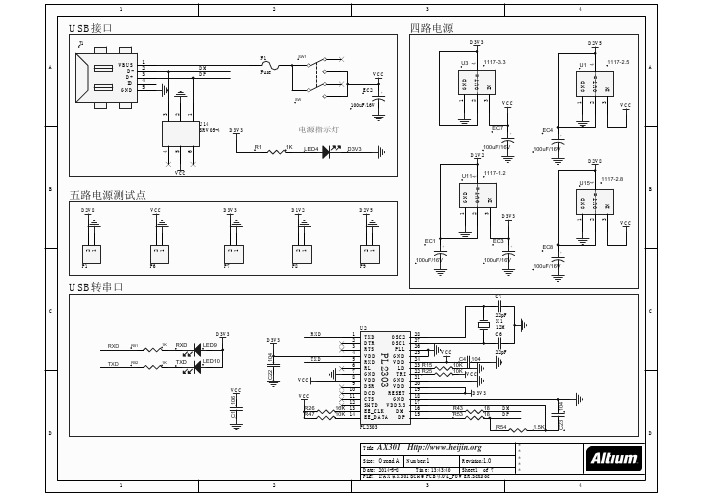
FPGA黑金开发板AX301原理图
BANK 5
U4F IO, DIFFIO_R4n, (INIT_DONE) IO, DIFFIO_R4p, (CRC_ERROR) IO IO, DIFFIO_R3n, (nCEO) IO, DIFFIO_R3p, (CLKUSR) IO, (DQS0R/CQ1R,DPCLK5)/(DQS0R/CQ1R,DPCLK5) IO, VREFB6N0 IO, DIFFIO_R2n IO, DIFFIO_R2p IO IO, DIFFIO_R1n, (DQS2R/CQ3R)/(DQS2R/CQ3R) IO, DIFFIO_R1p G16 G15 F13 F16 F15 B16 F14 D16 D15 G11 C16 C15 G16 LED0 F13 LED1 LED2 VGAD1 F14 LED3 VGA_VSYNC G11 VGA_HSYNC VGAD0
1
2
3
4
USB接口
J1 1 2 3 4 5 F1 DM DP Fuse EC2
SW SW1
四路电源
D3V3 D2V5
1117-3.3 1117-2.5
A
VBUS DD+ ID GND
U3
4
U1
4
A
OUT =
OUT = 2
VCC GND
+
GND
IN
1
2
3
100uF/16V 3 2 1 U14 SRV05-4
28 27 26 25 24 23 R15 22 R25 21 20 19 18 17 16 15
22pF
PL2303
C22
D3V3
R43 R53 18 18
DM DP
104
D
AT91SAM7X 开发板原理图 schematics
AT91SAM7X-EKEvaluation Boardfor AT91SAM7X and AT91SAM7XC .............................................................................................. User GuideTable of ContentsSection 1 Overview...............................................................................................1-11.1Scope........................................................................................................1-11.2Deliverables..............................................................................................1-11.3The AT91SAM7X-EK Evaluation Board....................................................1-1Section 2Setting Up the AT91SAM7X-EKEvaluation Board..................................................................................2-12.1Electrostatic Warning................................................................................2-12.2Requirements............................................................................................2-12.3Layout.......................................................................................................2-22.4Powering Up the Board.............................................................................2-32.5Getting Started..........................................................................................2-32.6AT91SAM7X-EK Block Diagram...............................................................2-4Section 3Board Description.................................................................................3-13.1AT91SAM7X Microcontroller.....................................................................3-13.2AT91SAM7X Block Diagram.....................................................................3-43.3AT91SAM7XC Microcontroller..................................................................3-53.4AT91SAM7XC Export Regulations Statement..........................................3-73.5AT91SAM7XC Block Diagram..................................................................3-83.6Memory.....................................................................................................3-93.7Clock Circuitry...........................................................................................3-93.8Reset Circuitry..........................................................................................3-93.9Power Supply Circuitry..............................................................................3-93.10Remote Communication...........................................................................3-93.11Analog Interface........................................................................................3-93.12User Interface...........................................................................................3-93.13Debug Interface......................................................................................3-103.14Expansion Slot........................................................................................3-10Section 4Configuration Straps.............................................................................4-14.1Configuration Straps.................................................................................4-1Section 5 Schematics...........................................................................................5-15.1Schematics...............................................................................................5-1Section 6 Errata....................................................................................................6-16.1Errata........................................................................................................6-1Section 7Revision History....................................................................................7-17.1Revision History........................................................................................7-1Section 1Overview 1.1Scope The AT91SAM7X-EK and the AT91SAM7XC-EK evaluation kits enable evaluation capa-bilities and code development of applications running on the AT91SAM7X or theAT91SAM7XC microcontroller.This guide focuses on the AT91SAM7X-EK board as a common evaluation platform forthe AT91SAM7X and AT91SAM7XC devices in a 100-lead LQFP package.1.2Deliverables The package contains the following items:!a board marked AT91SAM7X-EK!one A/B-type USB cable!one crossed serial RS232 cable!one RJ45 crossed Ethernet cable!universal input AC/DC power supply with US and EU plug adapter!one DVD-ROM containing summary and full datasheets, datasheets with electricaland mechanical characteristics, application notes and getting started documents forall development boards and AT91 microcontrollers. An AT91 software package with Cand assembly listings is also provided. This allows the user to begin evaluating theAT91 ARM® Thumb® 32-bit microcontroller quickly.1.3The AT91SAM7X-EK EvaluationBoard Depending on the model of the kit, the board is equipped with either an AT91SAM7X256 or an AT91SAM7XC256 (100-pin LQFP Green package) together with the following interfaces:!USB device port!DBGU serial communication port!RS232 serial communication port with RTS/CTS!JTAG/ICE debug interface connector!serial CAN communication ports!MII Ethernet 100-base TX with auto MDIX capability!buffered analog input and PWM outputOverview!Power LED and general-purpose LEDs!DataFlash® card slot!expansion connector!Atmel® serial DataFlash!One footprint for Atmel Serial EEPROM (MN11)Section 2 Setting Up the AT91SAM7X-EKEvaluation Board2.1ElectrostaticWarning The AT91SAM7X-EK evaluation board is shipped in a protective anti-static package. The board must not be subjected to high electrostatic potentials. A grounding strap or similar protective device should be worn when handling the board. Avoid touching the component pins or any other metallic element.2.2Requirements In order to set up the AT91SAM7X-EK evaluation board, the following items arerequired:!the AT91SAM7X-EK evaluation board itself!an A/B-type USB cableor!a DC USB power adapter (5V at 0.5 A) with USB A/B cableNote:The kit is not delivered with a JTAG/ICE interface which is required to start eval-uating the device.Setting Up the AT91SAM7X-EK Evaluation Board 2.3LayoutFigure 2-1. Layout - Top ViewSetting Up the AT91SAM7X-EK Evaluation Board Figure 2-2. Layout - Bottom View2.4Powering Up theThe AT91SAM7X-EK board is self-powered by the USB port or by a USB power adapter.Board2.5Getting Started The AT91SAM7X-EK evaluation board is delivered with a DVD-ROM containing all nec-essary information and step-by-step procedures for working with the most commondevelopment tool chains. Please refer to this DVD-ROM, or to the AT91 web site,/products/AT91/, for the most up-to-date information on gettingstarted with the evaluation kit.Setting Up the AT91SAM7X-EK Evaluation Board 2.6AT91SAM7X-EKBlock DiagramFigure 2-3. Block DiagramAT91SAM7X-EK Evaluation Board User Guide3-1Section 3Board Description3.1AT91SAM7X Microcontroller!Incorporates the ARM7TDMI ® ARM ® Thumb ® Processor–High-performance 32-bit RISC Architecture –High-density 16-bit Instruction Set –Leader in MIPS/Watt–EmbeddedICE ™, Debug Communication Channel Support !Internal High-speed Flash–256 Kbytes (AT91SAM7X256) Organized in 1024 Pages of 256 Bytes –128 Kbytes (AT91SAM7X128) Organized in 512 Pages of 256 Bytes –Single Cycle Access at Up to 30 MHz in Worst Case Conditions–Prefetch Buffer Optimizing Thumb Instruction Execution at Maximum Speed –Page Programming Time: 6 ms, Including Page Auto-erase,Full Erase Time: 15 ms –10,000 Write Cycles, 10-year Data Retention Capability,Sector Lock Capabilities, Flash Security Bit –Fast Flash Programming Interface for High Volume Production !Internal High-speed SRAM, Single-cycle Access at Maximum Speed–64 Kbytes (AT91SAM7X256)–32 Kbytes (AT91SAM7X128)!Memory Controller (MC)–Embedded Flash Controller, Abort Status and Misalignment Detection !Reset Controller (RSTC)–Based on Power-on Reset Cells and Low-power Factory-calibrated Brownout Detector –Provides External Reset Signal Shaping and Reset Source Status !Clock Generator (CKGR)–Low-power RC Oscillator, 3 to 20 MHz On-chip Oscillator and one PLL !Power Management Controller (PMC)Board Description–Power Optimization Capabilities, Including Slow Clock Mode (Down to 500 Hz)and Idle Mode–Four Programmable External Clock Signals!Advanced Interrupt Controller (AIC)–Individually Maskable, Eight-level Priority, Vectored Interrupt Sources–Two External Interrupt Sources and One Fast Interrupt Source, SpuriousInterrupt Protected!Debug Unit (DBGU)–2-wire UART and Support for Debug Communication Channel interrupt,Programmable ICE Access Prevention!Periodic Interval Timer (PIT)–20-bit Programmable Counter plus 12-bit Interval Counter!Windowed Watchdog (WDT)–12-bit key-protected Programmable Counter–Provides Reset or Interrupt Signals to the System–Counter May Be Stopped While the Processor is in Debug State or in IdleMode!Real-time Timer (RTT)–32-bit Free-running Counter with Alarm–Runs Off the Internal RC Oscillator!Two Parallel Input/Output Controllers (PIO)–Sixty-two Programmable I/O Lines Multiplexed with up to Two Peripheral I/Os–Input Change Interrupt Capability on Each I/O Line–Individually Programmable Open-drain, Pull-up Resistor and SynchronousOutput!Thirteen Peripheral DMA Controller (PDC) Channels!One USB 2.0 Full Speed (12 Mbits per second) Device Port–On-chip T ransceiver, 1352-byte Configurable Integrated FIFOs!One Ethernet MAC 10/100 base-T–Media Independent Interface (MII) or Reduced Media Independent Interface(RMII)–Integrated 28-byte FIFOs and Dedicated DMA Channels for Transmit andReceive!One Part 2.0A and Part 2.0B Compliant CAN Controller–Eight Fully-programmable Message Object Mailboxes, 16-bit Time StampCounter!One Synchronous Serial Controller (SSC)–Independent Clock and Frame Sync Signals for Each Receiver andTransmitter–I²S Analog Interface Support, Time Division Multiplex Support–High-speed Continuous Data Stream Capabilities with 32-bit Data TransferBoard Description!Two Universal Synchronous/Asynchronous Receiver Transmitters (USART)–Individual Baud Rate Generator, IrDA® Infrared Modulation/Demodulation–Support for ISO7816 T0/T1 Smart Card, Hardware Handshaking, RS485 Support–Full Modem Line Support on USART1!Two Master/Slave Serial Peripheral Interfaces (SPI)–8- to 16-bit Programmable Data Length, Four External Peripheral Chip Selects!One Three-channel 16-bit Timer/Counter (TC)–Three External Clock Inputs, Two Multi-purpose I/O Pins per Channel–Double PWM Generation, Capture/Waveform Mode, Up/Down Capability!One Four-channel 16-bit Power Width Modulation Controller (PWMC)!One Two-wire Interface (TWI)–Master Mode Support Only, All T wo-wire Atmel EEPROMs Supported!One 8-channel 10-bit Analog-to-Digital Converter, Four Channels Multiplexed with Digital I/Os!SAM-BA™ Boot Assistance–Default Boot program–Interface with SAM-BA Graphic User Interface!IEEE® 1149.1 JT AG Boundary Scan on All Digital Pins!5V-tolerant I/Os, Including Four High-current Drive I/O lines, Up to 16 mA Each!Power Supplies–Embedded 1.8V Regulator, Drawing up to 100 mA for the Core and External Components–3.3V VDDIO I/O Lines Power Supply, Independent 3.3V VDDFLASH Flash Power Supply–1.8V VDDCORE Core Power Supply with Brownout Detector!Fully Static Operation: Up to 55 MHz at 1.65V and 85°C Worst Case Conditions!Available in a 100-lead LQFP Green PackageBoard Description3.2AT91SAM7XBlock Diagram Figure 3-1. Block DiagramBoard Description3.3AT91SAM7XCMicrocontroller !Incorporates the ARM7TDMI® ARM® Thumb® Processor–High-performance 32-bit RISC Architecture–High-density 16-bit Instruction Set–Leader in MIPS/Watt–EmbeddedICE™, Debug Communication Channel Support!Internal High-speed Flash–256 Kbytes (AT91SAM7XC256) Organized in 1024 Pages of 256 Bytes–128 Kbytes (AT91SAM7XC128) Organized in 512 Pages of 256 Bytes–Single Cycle Access at Up to 30 MHz in Worst Case Conditions–Prefetch Buffer Optimizing Thumb Instruction Execution at Maximum Speed –Page Programming Time: 6 ms, Including Page Auto-erase,Full Erase Time: 15 ms–10,000 Write Cycles, 10-year Data Retention Capability,Sector Lock Capabilities, Flash Security Bit–Fast Flash Programming Interface for High Volume Production!Internal High-speed SRAM, Single-cycle Access at Maximum Speed –64 Kbytes (AT91SAM7XC256)–32 Kbytes (AT91SAM7XC128)!Memory Controller (MC)–Embedded Flash Controller, Abort Status and Misalignment Detection!Reset Controller (RSTC)–Based on Power-on Reset Cells and Low-power Factory-calibrated Brownout Detector–Provides External Reset Signal Shaping and Reset Source Status!Clock Generator (CKGR)–Low-power RC Oscillator, 3 to 20 MHz On-chip Oscillator and one PLL!Power Management Controller (PMC)–Power Optimization Capabilities, Including Slow Clock Mode (Down to 500 Hz) and Idle Mode–Four Programmable External Clock Signals!Advanced Interrupt Controller (AIC)–Individually Maskable, Eight-level Priority, Vectored Interrupt Sources–Two External Interrupt Sources and One Fast Interrupt Source, Spurious Interrupt Protected!Debug Unit (DBGU)–2-wire UART and Support for Debug Communication Channel interrupt, Programmable ICE Access Prevention!Periodic Interval Timer (PIT)–20-bit Programmable Counter plus 12-bit Interval Counter!Windowed Watchdog (WDT)Board Description–12-bit key-protected Programmable Counter–Provides Reset or Interrupt Signals to the System–Counter May Be Stopped While the Processor is in Debug State or in IdleMode!Real-time Timer (RTT)–32-bit Free-running Counter with Alarm–Runs Off the Internal RC Oscillator!Two Parallel Input/Output Controllers (PIO)–Sixty-two Programmable I/O Lines Multiplexed with up to Two Peripheral I/Os–Input Change Interrupt Capability on Each I/O Line–Individually Programmable Open-drain, Pull-up Resistor and SynchronousOutput!Seventeen Peripheral DMA Controller (PDC) Channels!One Advanced Encryption System (AES)–128-bit Key Algorithm, Compliant with FIPS PUB 197 Specifications–Buffer Encryption/Decryption Capabilities with PDC!One Triple Data Encryption System (TDES)–Two-key or Three-key Algorithms, Compliant with FIPS PUB 46-3Specifications–Optimized for Triple Data Encryption Capability!One USB 2.0 Full Speed (12 Mbits per second) Device Port–On-chip T ransceiver, 1352-byte Configurable Integrated FIFOs!One Ethernet MAC 10/100 base-T–Media Independent Interface (MII) or Reduced Media Independent Interface(RMII)–Integrated 28-byte FIFOs and Dedicated DMA Channels for Transmit andReceive!One Part 2.0A and Part 2.0B Compliant CAN Controller–Eight Fully-programmable Message Object Mailboxes, 16-bit Time StampCounter!One Synchronous Serial Controller (SSC)–Independent Clock and Frame Sync Signals for Each Receiver andTransmitter–I²S Analog Interface Support, Time Division Multiplex Support–High-speed Continuous Data Stream Capabilities with 32-bit Data Transfer!Two Universal Synchronous/Asynchronous Receiver Transmitters (USART)–Individual Baud Rate Generator, IrDA® Infrared Modulation/Demodulation–Support for ISO7816 T0/T1 Smart Card, Hardware Handshaking, RS485Support–Full Modem Line Support on USART1!Two Master/Slave Serial Peripheral Interfaces (SPI)Board Description–8- to 16-bit Programmable Data Length, Four External Peripheral Chip Selects!One Three-channel 16-bit Timer/Counter (TC)–Three External Clock Inputs, Two Multi-purpose I/O Pins per Channel–Double PWM Generation, Capture/Waveform Mode, Up/Down Capability!One Four-channel 16-bit Power Width Modulation Controller (PWMC)!One Two-wire Interface (TWI)–Master Mode Support Only, All T wo-wire Atmel EEPROMs Supported!One 8-channel 10-bit Analog-to-Digital Converter, Four Channels Multiplexed with Digital I/Os!SAM-BA™ Boot Assistance–Default Boot program–Interface with SAM-BA Graphic User Interface!IEEE® 1149.1 JT AG Boundary Scan on All Digital Pins!5V-tolerant I/Os, Including Four High-current Drive I/O lines, Up to 16 mA Each!Power Supplies–Embedded 1.8V Regulator, Drawing up to 100 mA for the Core and External Components–3.3V VDDIO I/O Lines Power Supply, Independent 3.3V VDDFLASH Flash Power Supply–1.8V VDDCORE Core Power Supply with Brownout Detector!Fully Static Operation: Up to 55 MHz at 1.65V and 85°C Worst Case Conditions!Available in a 100-lead LQFP Green Package3.4AT91SAM7XCExportRegulationsStatement These commodities, technology or software will be exported from France and the appli-cable Export Administration Regulations will apply. French, United States and other relevant laws, regulations and requirements regarding the export of products may restrict sale, export and re-export of these products; please assure you conduct your activities in accordance with the applicable relevant export regulations.Board Description3.5AT91SAM7XCBlock Diagram Figure 3-2. Block DiagramBoard Description3.6Memory!256 Kbytes of Internal High-speed Flash!64 Kbytes of Internal High-speed SRAM!Atmel serial DataFlash®!One footprint for Atmel Serial EEPROM memory. The user can fit an AT24C128AN orAT24C256AN or AT24C512AN in 8S1 package as well as a cryptomemoryAT88C25616C-SI3.7Clock Circuitry!18.432 MHz standard crystal for the embedded oscillator!32 KHz internal RC oscillator3.8Reset Circuitry!Internal reset controller with a bidirectional reset pin!External reset pushbutton3.9Power SupplyCircuitry !USB powered, the dynamic power consumption on VDDCORE is less than 90 mA at full speed when running out of the Flash. The total current at power-up is less than 100 mA.!External power can be applied via USB Power adapter 5V 0.5A with USB A/B cable !On-chip embedded VDDCORE 1.8V regulator!On-board 3.3V 400 mA linear regulator3.10RemoteCommunication !One Serial interface (DBGU COM Port) via RS-232 DB9 male socket!One Serial interface (RS232 COM Port) via RS-232 DB9 male socket!USB V2.0 Full-speed compliant, 12 Mbits per second (UDP)!One CAN 2.0B communication port via the 3-position printed circuit terminal block !One MII Ethernet 100-base TX (auto MDI/MDI-X crossover cable)3.11Analog Interface!One selectable 0.2% 3.00V Vref or 3.3V ANA!One 3-position printed circuit terminal block!Two analog up to Vref inputs. One external user input and one back-looped withbuffered PWM3 output.!One buffered PWM3 analog output (up to Vref)3.12User Interface!One 5-way joystick (4 directions and push for confirmation)!Four general-purpose buffered green user LEDs (PWM controlled)Board Description!One yellow power LED (can also be software controlled)3.13Debug Interface!20-pin JTAG/ICE interface connector!DBGU serial RS232 COM Port3.14Expansion Slot!One DataFlash card slot!All I/Os of the AT91SAM7X and the AT91SAM7XC are routed to peripheral extensionconnectors (J16). This allows the developer to check the integrity of the componentsand to extend the features of the board by adding external hardware components orboards.AT91SAM7X-EK Evaluation Board User Guide4-16195E–ATARM–22-Mar-07Section 4Configuration Straps4.1Configuration StrapsTable 4-1. Configuration Jumpers and StrapsDesignationDefault Setting FeatureJ8OpenedErases all internal Flash memory when the board ispowered. To do that, the user will have to close the J8 at least 200 ms.J9Opened Do not use: Factory test mode. J9 is not populated J10Opened Selects ICE mode or JTAG mode (Closed). J10 is not populated.J11Closed VDDIN Jumper (1)J12Closed VDDFLASH Jumper (1)J131-2ADVREF Jumper select 1-2: 3.00V Voltage reference 2-3: VDDANA J14Closed VDDCORE Jumper (1)J15Closed VDDIO Jumper (1)J17OpenedExternal XIN clock input. S4 and S5 must be open. J17 is not populated.J18Closed VDDPLL Jumper (1)J19Closed Enables the use of the NPCS00 (P A12).J21Closed Enables 120 ohms CAN bus resistance termination.J28Closed Enables Ethernet Auto MDIX control.S1Closed Enables permanent pull up on USB DP .S2Closed The System Reset signal (NRST) is connected to the ICE/JTAG socket (J7, pin 15).S3OpenedDisables 5V (VUSB) power supply on J16 extension connector.Configuration Straps6195E–ATARM–22-Mar-07Note:1.These jumpers are provided for measuring power consumption. By default, they areclosed. T o use this feature, the user has to open the strap and insert an anmeter.S4 - S5Closed Enables the use of 18.432MHz crystal. Must be open if an external clock is used.S6Closed Enables the Power Led control (PB25).S7Opened Disables Serial DataFlash write protect.S8Closed Enables the use of the TXD CAN transceiver (P A20)S9Closed Enables the use of the RXD CAN transceiver (P A19)S10Closed Enables control of the Standby/Normal mode for CAN transceivers (P A2)S11OpenedEnables control of the Standby/Normal mode for CAN transceivers (P A2).If S11 is closed, S10 must be open.S12Closed Enables the use of PWM3 Analog Output (PB30)S13Closed Enables the use of the TXD0 signal (P A1)S14Closed Enables the use of the RTS0 signal (P A3)S15Closed Enables the use of the RXD0 signal (P A0)S16Closed Enables the use of the CTS0 signal (P A4)S17Closed Enables the use of the User LED DS1 (PB19)S18Closed Enables the use of the User LED DS2 (PB20)S19Closed Enables the use of the User LED DS3 (PB21)S20Closed Enables the use of the User LED DS4 (PB22)S21Closed Enables the use of the DBGU TXD signal (P A28)S22Closed Enables the use of the DBGU RXD signal (P A27)S23Opened ETHERNET MII is the default mode. To evaluate the RMII mode, the user change S23 to S26 configuration in the following way: S23 Closed, S24 Opened, S25 Closed, S26 Opened S24Closed S25Opened S26Closed S27Opened ReservedS28Closed Enables the use of the SCL of MN11 (P A11)S29Closed Enables the use of the SDA of MN11 (P A10)TP1N.A GND T est point.TP2N.AGND T est point.Table 4-1. Configuration Jumpers and Straps (Continued)Designation Default Setting FeatureAT91SAM7X-EK Evaluation Board User Guide5-16195E–ATARM–22-Mar-07Section 5Schematics5.1SchematicsThis section contains the following schematics:!Processor Board !I/O !Ethernet !RF modulesSchematics6195E–ATARM–22-Mar-07AT91SAM7X-EK Evaluation Board User Guide6-16195E–ATARM–22-Mar-07Section 6Errata6.1DM9161A Ethernet Phy ConnectionsThe Ethernet interface works as presented in the schematics, but the connections are not in compliance with Davicom recommendations.To comply with Davicom recommendations on connecting this device, J27-4 and J27-5(RJ45 connector, CT) should be connected to the VCCA side of L2. In the current sche-matics (ETHERNET, Sheet 3/4), the VCCA side of L2 is connected to MN10-1 and MN10-2 (DM9161A, AVDDR).For additional information, refer to the Davicom datasheet for DM9161A and associated Application Notes available on /.6.2TWI line pullups for Fast Mode operationIn order to use the TWI in Fast Mode (up to 400 Kbits/s), the default 10 K Ω resistors R38and R39 should be replaced by smaller values (e.g., 2.2 K Ω).Note that there is no need to change the pull-up resistors if the TWI is used in Standard Mode (up to 100 Kbits/s).Errata6195E–ATARM–22-Mar-07AT91SAM7X-EK Evaluation Board User Guide7-16195E–ATARM–22-Mar-07Section 7Revision History7.1Revision HistoryTable 7-1. Change HistoryDocument Comments Change Request Ref.6195A First issue.6195B Updated Figure 2-3 with new signal names. Updated document to show new product functionalities. New board block diagram and schematics issued.05-4306195C Updated document to contain new product A T91SAM7XC.Added new section with Errata.6195D Removed references to 32 Mbit serial DataFlash (A T45DB321C-CNC) in Section 1.3 and in Section 3.6. Inserted new Figure 2-3 and new schematics in Section 5. 28626195EAdded Errata Section 6.2 ”TWI line pullups for Fast Mode operation”4084Revision History6195E–ATARM–22-Mar-07Disclaimer: The information in this document is provided in connection with Atmel products. No license, express or implied, by estoppel or otherwise,to any intellectual property right is granted by this document or in connection with the sale of Atmel products. EXCEPT AS SET FORTH IN ATMEL ’S TERMS AND CONDI-TIONS OF SALE LOCATED ON ATMEL ’S WEB SITE, ATMEL ASSUMES NO LIABILITY WHATSOEVER AND DISCLAIMS ANY EXPRESS, IMPLIED OR STATUTORY WARRANTY RELATING TO ITS PRODUCTS INCLUDING, BUT NOT LIMITED TO, THE IMPLIED WARRANTY OF MERCHANTABILITY, FITNESS FOR A PARTICULAR PURPOSE, OR NON-INFRINGEMENT. IN NO EVENT SHALL ATMEL BE LIABLE FOR ANY DIRECT, INDIRECT, CONSEQUENTIAL, PUNITIVE, SPECIAL OR INCIDEN-TAL DAMAGES (INCLUDING, WITHOUT LIMITATION, DAMAGES FOR LOSS OF PROFITS, BUSINESS INTERRUPTION, OR LOSS OF INFORMATION) ARISING OUT OF THE USE OR INABILITY TO USE THIS DOCUMENT, EVEN IF ATMEL HAS BEEN ADVISED OF THE POSSIBILITY OF SUCH DAMAGES. Atmel makes no representations or warranties with respect to the accuracy or completeness of the contents of this document and reserves the right to make changes to specifications and product descriptions at any time without notice. Atmel does not make any commitment to update the information contained herein. Unless specifically provided otherwise, Atmel products are not suitable for, and shall not be used in, automotive applications. Atmel’s products are not intended, authorized, or warranted for use as components in applications intended to support or sustain life.Atmel CorporationAtmel Operations2325 Orchard Parkway San Jose, CA 95131, USA Tel: 1(408) 441-0311Fax: 1(408) 487-2600Regional HeadquartersAtmel EuropeLe Krebs8, rue Jean-Pierre Timbaud BP 30978054 Saint-Quentin-en-Yvelines Cedex FranceTel: (33) 1-30-60-70-00 Fax: (33) 1-30-60-71-11AsiaRoom 1219Chinachem Golden Plaza 77 Mody Road Tsimshatsui East Kowloon Hong KongTel: (852) 2721-9778Fax: (852) 2722-1369Japan9F, Tonetsu Shinkawa Bldg.1-24-8 ShinkawaChuo-ku, Tokyo 104-0033JapanTel: (81) 3-3523-3551Fax: (81) 3-3523-7581Memory2325 Orchard Parkway San Jose, CA 95131, USA Tel: 1(408) 441-0311Fax: 1(408) 436-4314Microcontrollers2325 Orchard Parkway San Jose, CA 95131, USA Tel: 1(408) 441-0311Fax: 1(408) 436-4314La Chantrerie BP 7060244306 Nantes Cedex 3, France Tel: (33) 2-40-18-18-18Fax: (33) 2-40-18-19-60ASIC/ASSP/Smart CardsZone Industrielle13106 Rousset Cedex, France Tel: (33) 4-42-53-60-00Fax: (33) 4-42-53-60-011150 East Cheyenne Mtn. Blvd.Colorado Springs, CO 80906, USA Tel: 1(719) 576-3300Fax: 1(719) 540-1759Scottish Enterprise Technology Park Maxwell BuildingEast Kilbride G75 0QR, Scotland Tel: (44) 1355-803-000Fax: (44) 1355-242-743RF/AutomotiveTheresienstrasse 2Postfach 353574025 Heilbronn, Germany Tel: (49) 71-31-67-0Fax: (49) 71-31-67-23401150 East Cheyenne Mtn. Blvd.Colorado Springs, CO 80906, USA Tel: 1(719) 576-3300Fax: 1(719) 540-1759BiometricsAvenue de Rochepleine BP 12338521 Saint-Egreve Cedex, France Tel: (33) 4-76-58-47-50Fax: (33) 4-76-58-47-60Literature Requests/literature© 2007 Atmel Corporation. All rights reserved. Atmel ®, logo and combinations thereof, and Everywhere You Are ®, DataFlash ® and others are registered trademarks, SAM-BA ™ and others are trademarks of Atmel Corporation or its subsidiaries. ARM ®, the ARM Powered ® logo,ARM7TDMI ®, Thumb ® and others are the registered trademarks or trademarks of ARM Ltd. Other terms and product names may be trademarks of others.6195E–ATARM–22-Mar-07。
开发板分块原理图

预备知识单片机在一片集成电路芯片上集成微处理器、存储器、I/O接口电路,从而构成了单芯片微型计算机,即单片机。
Intel公司推出了MCS-51系列单片机:集成8位CPU、4K字节ROM、128字节RAM、4个8位并口、1个全双工串行口、2个16位定时/计数器。
寻址范围64K,并有控制功能较强的布尔处理器。
字节和位字节(byte)位(bit)一个位只能表示0或1一字节(byte)=8位(bit)平时说的1KB ,1MB, 1GB 单位都是byte ,1KB =1024 Byte 1M=1024KB 1GB=1024MB关于电平特性数字电路中只有两种电平:高和低(本课程中)定义单片机为TTL电平:高+5V 低0VRS232电平:计算机的串口高-12V 低+12V所以计算机与单片机之间通讯时需要加电平转换芯片max232。
进制:二进制,16进制,二进制0 1十进制:0 1 2 3 4 5 6 7 8 9十六进制:0 1 2 3 4 5 6 7 8 9 A B C D E请大家记住:在程序中每4个二进制数可以用1个16进制数表示比如9(16)= 1001(2)B(16)=1011(2)F(16)=1111(2)刚开始学你定要自己算,当然可以借助辅助工具:在程序中二进制数用“0b” 表示,16进制数用”0x”表示,10进制为默认表示,前面啥都不加。
比如0b00000010 = 0x02= 2逻辑运算:1. “位与”运算“与”运算是实现“必须都有,否则就没有”这种逻辑关系的一种运算。
运算符为“· ”, 其运算规则如下:0·0=0, 0·1=1·0=0, 1·1=1在C 语言运算符中,位与用“&”表示例子:0b00110000 & 0b00000010=0b00000000=02. “位或”运算“或”运算是实现“只要其中之一有,就有”这种逻辑关系的一种运算, 其运算符为“+”。
【GL9型51单片机开发学习系统】原理图集V7.1

02
CN12
102
102
7 6 5 4 3 2 1 0
+
U4
AT24C02
有源蜂鸣器
无源蜂鸣器
AMS1117 3.3 K020
C9
R66
102
102
U1
W25Q16
P00
P0 7
P27
P20
给力者
R
N N N 4 3 2 1 0
C7
74HC138
FLASH存储器
103
16×16 LED点阵屏
U14
U13
V1 V2 V3 V4 V5 V6 V7 V8
R9-R12
331 331 331 331
LED1
R13-R16
331 331 331 331
LED2
U16
CN24
ULN2003
R69
R1 R2 R3 R4 R5 R6 R7 R8
331 331 331 331 331 331 331 331
CN28
液晶接口 液晶接口
1602
CN26 VR3 CN27
VR2
K A Vlcd RST CS2 CS1 DB7 CN29 DB6 h g DB5 DB4 f DB3 e DB2 d DB1 c DB0 b E a 1位静态数码管 R/W RS Vo Vdd Vss
331 331 331 331 331 331
1000 16V RVT
FU
USB-串口单元 备用电源接口
CN7
10 3
10 3
101
10 3
101
10 3
CN3
331
U3
E3
红牛开发板stm32f103zet6用户手册

红牛开发板用户手册 CopyRight@20091.概述红牛STM32开发板是以意法半导体 (ST)公司推出的基于ARM Cortex-M3系列最高配置芯片STM32F103ZE为核心组成。
板上资源:●CPU:STM32F103ZET6;(LQFP144脚,片上集成512K flash、64KRAM、12Bit ADC、DAC、PWM、CAN、USB、SDIO、FSMC等资源)●板上外扩512K SRAM, 2M NOR FLASH (板上支持最大1024kSRAM,16M的NOR FLASH)满足大容量数据采集、处理及分析要求●板上外扩128M或256M NAND FLASH(标配128M)满足彩屏上丰富的图片存储、数据表格存储,文件管理等应用● 搭配2.8寸TFT真彩触摸屏模块或3.2寸TFT真彩触摸屏模块(由用户选择),FSMC控制,彩屏模块上配置RSM1843(ADS7843、TSC2046脚对脚兼容)触摸控制器芯片,支持一个SD卡(SPI方式)可用于存储图片,支持一个AT45DBxxx 的DATA FLASH(可用于存储汉字库)● 一路CAN通信接口,驱动器芯片SN65VHD230● 两路RS232接口● 一路RS485通信接口● 一个SD卡座SDIO控制方式● 一个I2C存储器接口,标配24LC02(EEPROM)● 一个SPI存储器接口,标配AT45DB161D(DATA FLASH)● 一路ADC调节电位器输入● 三路ADC输入接线端子引出● 两路PWM输出接线端子引出● 两路DAC输出接线端子引出● 一个蜂鸣器、五个用户LED灯、一个电源指示灯,一个USB通信指示灯,● 四个用户按键,一个系统复位按键● 电源选择跳线,支持外接5V 电源供电,USB 供电或JLINK 供电 ● 板子规格尺寸:13CM X 10CM● 所有I/O 口通过2.54MM 标准间距引出,方便二次开发板上的全部硬件特性能快速帮助你评估STM32F103ZE 所有外设(USB 、motor control,、CAN,、SPI 、MicroSD card 、smartcard 、USART 、NOR Flash 、NAND flash 、 SRAM )和开发你自己的应用项目。
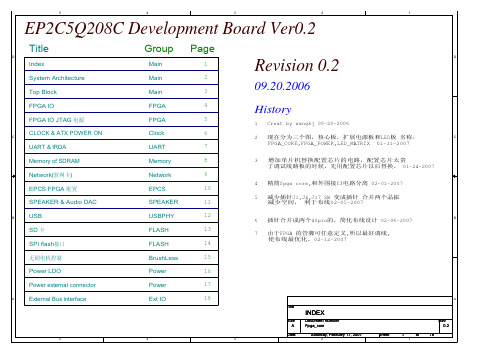
EP2C5Q208C开发板原理图
Rev 0.2 Sheet 2
1
of
18
5
4
3
2
1
10_POWER1
D
POWER
D
EXTIO1
EXTIO
FPGA1 IO_D[0..65]
CONFIG1 EPCS1/4 Data0 Dclk nCS0 ASDIO CONF_DONE nCONFIG nCE TDI TDO TMS TCK
IO_D[0..65]
DATA0 SD_CD SD_CLK SD_CMD SD_D[0..3] SPI_CS DCLK nCONFIG CONF_DONE nstatus UATXD1 UARXD1
A
BL[0..2] BrushLess_in1 BrushLess_in2 BrushLess_in3
USB PHY / pdownloads.cgi/list/usbhostslave POR 自包含reset电路?
USB1 PHY
nSDCAS nSDRAS nSDCS0 nSDWE
B
nSDCAS nSDRAS nSDCS0 nSDWE nWBE0 nWBE1 SDCLK SDCKE
USB_OE USB_SPEED USB_VM USB_VM0 USB_VP USB_VP0
USB_OE USB_SPEED USB_VM USB_VM0 USB_VP USB_VP0
5
4
3
2
1
EP2C5Q208C Development Board Ver0.2
Title
D
Group
Main Main Main FPGA FPGA Clock UART Memory Network EPCS SPEAKER USBPHY FLASH FLASH BrushLess Power Power Ext IO
- 1、下载文档前请自行甄别文档内容的完整性,平台不提供额外的编辑、内容补充、找答案等附加服务。
- 2、"仅部分预览"的文档,不可在线预览部分如存在完整性等问题,可反馈申请退款(可完整预览的文档不适用该条件!)。
- 3、如文档侵犯您的权益,请联系客服反馈,我们会尽快为您处理(人工客服工作时间:9:00-18:30)。
金牛开发板用户手册 CopyRight@20091.概述金牛嵌入式开发板采用STM32F107VC,是意法半导体推出全新STM32互连型(Connectivity)系列微控制器中的一款性能较强产品,此芯片集成了各种高性能工业标准接口,且STM32不同型号产品在引脚和软件上具有完美的兼容性,可以轻松适应更多的应用。
新STM32的标准外设包括10个定时器、两个12位1-Msample/s AD(模数转换器) (快速交替模式下2M sample/s)、两个12位DA(数模转换器)、两个I2C接口、五个USART接口和三个SPI端口和高质量数字音频接口IIS, 另外STM32F107拥有全速USB(OTG)接口,两路CAN2.0B接口,以及以太网10/100 MAC模块.此芯片可以满足工业、医疗、楼宇自动化、家庭音响和家电市场多种产品需求.开发板硬件配置:● STM32F107VC◆ 32位RISC性能处理器◆ 32位ARM Cortex-M3结构优化◆ 72 MHz 运行频率,1.25 DMIPS/MHz◆硬件除法和单周期乘法◆快速可嵌套中断,6~12个时钟周期◆具有MPU保护设定访问规则● 高达256KB Flash, 高达64KB的SRAM● 网络通信功能◆一个RJ45网络接口,支持10M/100M自适应网络◆一个RS485网络通讯接口◆两个CAN BUS网络通讯接口● 人机交互接口◆一个3.2寸或2.8寸大屏幕320*240,26万色TFT-LCD,支持8/16位总线接口,镜面屏,超高高度● 电阻式触摸屏,含专业高精度触摸屏控制芯片(RSM1843)● 四个LED 发光管指示,一个电源发光管指示● 两个GPIO 按键● 一个RESET 按键● 两个RS232串行通信接口(DB9)◆串口1用于通信,需设置跳线选择连接串口1◆串口2用于通信支持ISP,需设置跳线选择连接串口2● 一个mini AB型USB 插座,支持最新USB OTG技术,配备USB主机转接线,从机转接线◆ USB OTG功能,支持外接优盘● SPI接口◆一路连接DATAFLASH(AT45DB161D)◆一路连接到TFT模块的触摸驱动芯片(RSM1843)● IIC接口◆ IIC接口外接EEPROM(24LC02)● 一个SD 卡座SPI操作方式(不含SD卡),提供文件系统(FATFS)● 外接两路独立的ADC输入通道● 外接两路独立的DAC输出通道● 一路电位器输入模拟信号● 一个标准JTAG/SWD调试接口(20pin)● 供电方式: 5V电源适配器或USB供电,通过跳线选择● 引出芯片所有IO,方便二次开发2.电路及接口说明由于空间有限标注未能一一说明每个接口和IC的定义和功能,需详细接口定义资料请参考电路原理图。
2.1 Power supply(电源供给)金牛开发板采用外部5V电源输入、USB接口提供5V电源输入● 5V DC 电源适配器连接到CN15,电源选择跳线JP1插到1-2处。
选择外部5V电源供电。
● 把USB电缆连接到USB口CN7,电源选择跳线JP1插到2-3处,选择USB 5V 电源供电。
表1、电源选择跳线设置描述Jumper描述JP1 JP1用于选择外部5V电源座输入5V电源供电,USB供电。
跳线短路帽在1-2处为外部5V供电,2-3处为USB口供电。
2.2 Boot option(启动选项)金牛开发板可以采用以下启动方式:● Embedded user Flash (默认)● System memory with boot loader for ISP● Embedded SRAM for debugging启动方式通过配置BOOT1(JP13)和BOOT0(JP15)选择跳线设定。
表2、启动方式选择跳线设置描述BOOT1(JP13) BOOT0(JP15)启动模式描述ANY(1-2、2-3 or open)2-3 金牛开发板设定为User Flash 启动方式。
BOOT1可以任意位置,如插到1-2、2-3或是开路(既不插)默认是插到2-3(Defaultsetting)2-3 1-2 红牛开发板设定为System Memory启动方式。
1-2 1-2 红牛开发板设定为Embedded SRAM启动方式。
2.3 Clock source(时钟源)金牛开发板由两个时钟源提供系统时钟和RTC时钟。
Y1,32.768kHZ晶震,做为RTC的时钟源Y2,25MHZ晶震,做为系统的时钟源,如果采用内部8M RC震荡器Y2可以不接。
Y3,25MHZ晶震,做为以太网PHY的时钟。
Note: JP14为1-2时连接电源给RTC,当JP14为2-3时连接后备电池供电给RTC。
2.4、复位方式复位信号在金牛开发板上是低电平复位。
复位方式包括以下几种方式:复位按键Reset(S1)通过JTAG仿真下载口输入复位信号2.5 模拟输入CN14的AIN0、AIN1、连接到STM32F107VC的外部模拟输入引脚PB0、PB1上。
AD调节电位器输入VR1 连接到PC02.6 DAC输出CN14的DAC0、DAC1连接到STM32F107VC的DAC输出引脚PA4、PA5。
DAC0、DAC1输出引脚与SPI1_NSS、SPI1_SCK引脚复用。
如要使用DAC0和DAC1需要拔掉J9、J10跳线。
J9、J10跳线默认是插上,既分配给SPI1使用。
2.7 USB-OTG金牛开发板具有一个MINI USB AB型 USB OTG 全速接口(CN7)开发板可采用这个USB 口提供最大500mA的电源。
USB OTG VBUS线和ID线跟USART1 TX、RX数据线共用IO,开板当要使用USB-OTG功能时必须按下表设置跳线才能正确连接USB。
表3、 USB选择跳线接口描述JP3 JP5 描述1-2 1-2 金牛开发板设置连接到USB-OTG功能,即USB-OTG有效。
2.8 显示接口320X240 TFT彩色LCD数据线连接到STM32F107VC的PE口。
4个红色LED(LD2、3、4、5)连接到标准IO口PD2、3、4、7用于显示。
CN13 彩色TFT屏接口表4、彩色TFT LCD接口描述引脚定义如下:引脚 信号描述 对应IO 引脚信号描述对应IO引脚信号描对应IO述1 3V3 电源2 GND 地3 DB00 PE04 DB01 PE15 DB02 PE26 DB03 PE37 DB04 PE48 DB05 PE59 DB06 PE6 10 DB07 PE7 11 DB08 PE8 12 DB09 PE913 DB10 PE10 14 DB11 PE11 15 DB12 PE12 16 DB13 PE13 17 DB14 PE14 18 DB15 PE15 19 CS PC6 20 RS PD13 21 WR PD14 22 RD PD15 23 RESET RESET24 EN NC 25 MISO PC11 26 INT PC5 27 MOSI PC12 28 LE PB2 29 SCLK PC10 30 F_CS PC7 31 TP_CS PC8 32 SD_CS PC92.9 EEPROM连接到STM32F107VC的I2C1总线上,跳线JP11插入用于连接EEPROM24LC02EEPROM,拔出用于断开与EEPROM的硬件连接。
2.10 CAN金牛开发板支持两路CAN2.0A/B总线通信接口Note: JP11为开路状态时连接到CAN2,当短路JP11时为连接到I2C1总线。
2.11 RS-232和RS-485金牛开发板的一路RS-485通信接口CN3和两个RS-232通信接口CN5、CN6连接到STM32F107VC的USART1和USART2。
两个控制信号Bootloader_BOOT0 和Bootloader_RESET,也同时连接到CN6的RS-232接口上用于自动ISP烧写(无需设置BOOT0跳线)。
表 5. RS-232 跳线设置描述表5、 RS-232和RS-485选择跳线接口描述JP3 JP5 描述2-3 2-3 金牛开发板设置连接到USART1,即USART1有效JP4 描述1-2 金牛开发板设置USART2_RX连接到RS-4852-3 金牛开发板设置USART2_RX连接到RS-2322.12 SD card板上的SD卡接口连接到STM32F107VC的SPI1上。
SD卡的检测信号连接到标准IO口PB14,SD卡的电源控制信号连接到标准IO口PC4。
要使用SD卡功能必须短接JP9和JP10跳线。
表6、 SD卡选择跳线接口描述JP9 JP10 描述短路(close)短路(close)使能SD卡开路(open)开路(open)禁止使用SD卡2.13 Ethernet金牛开发板支持10M/100M以太网通信接口,采用PHY DP83848CVV (U8)和一个内带网络滤波器的RJ45连接座(CN8)。
通过跳线JP7、JP8、JP12、设置支持MII接口模式和RMII接口模式。
表7、以太网选择跳线接口描述跳线描述配置JP12 JP2 选择MII 或 RMII 接口模式。
. JP2开路选择MII接口模式, JP2短路选择RMII接口模式。
默认设置:开路OPENJP7当设置为MII接口模式时JP7插到2-3 (默认设置) 1-2当设置为RMII接口模式时JP7插到1-22-3JP8插到2-3时优先选择MCO(PA8)脚输出25 MHz 时钟给MII模式或50 MHz 时钟给RMII模式。
(默认设置 )2-3JP8插到1-2时优先选择晶震Y3提供25 MHz 时钟给MII接口模式。
1-2JP8JP8开路时优先选择外部有源晶震U8提供时钟(默认不装)OPEN Note: JP2, JP6默认设置是给以太网,在开始使用以太网功能时请检查这几个跳线的配置。
3、接口定义(Connectors)3.1 模拟输入、DAC输出接口CN14定义Pin number Description Pin number Description1 AIN0 4 DAC02 AIN1 5 DAC13 GND 6GND 3.2 CAN总线接口CN2定义Pin number Description PinnumberDescription1 3V3 4 CAN2H2 CAN1H 5 CAN2L3 CAN1L 6 GND 3.3 RS485总线接口CN3定义Pin number Description Pin number Description 1 485B 2 485A3.4 RS232通信接口CN5、CN6定义RS232 connector CON1、CON2 (front view)CN5定义Pin number Description Pin number Description1 NC 6 NC2 USART1_PA9 7 NC3 USART1_PA10 8 NC4 NC 9 NC5 GNDCN6定义Pin number Description Pin number Description1 NC 6 NC2 USART2_PD5 7 RTS (控制BOOT0)3 USART2_PD6 8 NC4 DTR(控制RESET)9 NC5 GND3.5 JTAG调试接口CN1 定义Pin number Description Pin number Description1 3.3V power2 3.3V power3 PB4 4 GND5 PA156 GND7 PA13 8 GND9 PA14 10 GND11 RTCK 12 GND13 PB3 14 GND15 RESET# 16 GND17 DBGRQ 18 GND19 DBGACK 20 GND3.6 USB MiniAB CN7USB连接座引脚定义如下:脚位编号功能描述脚位编号功能描述1 VBUS (PA9) 4 ID (PA10)2 D- (PA11) 5 GND3 D+ (PA12)3.7 以太网 RJ45 连接座 CN8以太网连接座CN8正面视图RJ45 connector CN8Pin number Description Pin number Description 1 TxData+ 2 TxData3 RxData+4 Shield5 Shield6 RxData7 Shield 8 Shield 3.8 SD card连接座 CN4Pin number Description PinnumberDescription1 SDcard_CS (PA4)7 SDcard_DOUT(PA6)2 SDcard_DIN(PA7) 8 NC3 Vss/GND 9 NC4 +3V3 10 SDcard_detect (PB14)5 SDcard_CLK (PA5)11 GND6 Vss/GND12 NC。