DS5000T-8-12中文资料
背涂改善单面涂布纸水翘曲问题

四.结论与建议
1.丁苯胶乳与氢氧化铝混合进行背涂后纸页水翘曲程度较小,虽碱液渗透性稍慢,但基 本能满足客户要求,可以作为解决标签涂布纸水翘曲问题的方法。
2.推荐试用的初始配方及方法:
初始 配 方 :丁苯胶乳
50份 (固体量计)
市售 A l(O H )3( } 2N ,m ) 1 7份 ( 固 体量 计)
华东七省市造纸学会第二十届造纸技术交流会暨中国造纸学会机械设备专业委员会年会
水翘 曲角度:水面与纸样边缘的夹角。 .水翘曲高度:水面与纸样边缘的垂直高度。 e.碱液渗透性:将纸样折成小船状,使其漂浮在3%的氢氧化钠溶液的同时在纸面
上滴 加 一 滴酚酞 (背涂面朝碱液),同时开始计时,测量酚酞开始变红的时间。
涂料 液 的 固 含 量 以 控 制 涂 布量 和 方 便操作为准。
涂布 量 : 2g/m2左右(背面)
涂 布方 式 :表面施胶
3. 配 方 及方法的说明: (1 )该 配 方是以实验室试验为基础的推荐试用的初始配方,需要在生产过程中根据实际 情况加以调整,使之逐步完善、成熟。 (2 )涂 布 量要求的是背面必须达到的量,至于正面可以有几种选择:使用原有表面施胶 的配方、使用本配方双面涂布、不进行表面施胶。可通过试验确定正面施胶的最佳方式。
90 9 7.8
无无
以上 是 在 实验室大量试验的基础上筛选出比较好的颜胶比配方的比较。试验认为:颜料 量增加时翘曲程度随之提高,渗碱时间减短;颜料量减少时则反之。
本试 验 采 用的是聚合物涂层封堵的原理改善水翘曲情况,因此涂层的增加会导致碱液渗 透性在一定程度上变差是必然的;但涂层量过低则可能导致涂层不完整,从而达不到封堵水
一、纸样分析
顶松DS822-T3 重量变送器 使用说明书

DS822-T3 重量变送器使用说明书杭州顶松自控设备有限公司浙制00000505号前言承蒙您此次购买DS822-T3型变送器,请接受我们真诚的谢意。
为了使您能够正确地使用该变送器,充分发挥DS822-T3型变送器优越的性能,希望您在使用本变送器之前,务必详细阅读本使用说明书。
本说明书在编写当中,虽然力求完善无误,但是难免有疑点、错误和遗漏之处,当您发现时,敬请告知,谢谢各位的支持。
主要功能⑴称重高精度、高稳定,可分辨0.2uV;⑵1路隔离的4-20mA模拟输出,精度可达0.05%;⑶同时具有隔离的232通讯接口和隔离的485接口,同时具有顶松的通讯协议和标准的MODBUS RTU总线协议;⑷称重测量具有长线补偿能力;⑸不用砝码也能标定,计算方法简单;⑹完备的自检功能;主要性能⑺ A/D输入信号范围:-40mV/V~+40mV/V⑻ A/D内部分辨率:1/100万⑼ A/D转换速度:100次/秒⑽ A/D非线性:<0.003%FS⑾增益漂移:2PPM/℃(TYP)⑿传感器供桥电源: DC5V,I>100mA可连接6个350Ω的传感器的传感器⒀输出资源:1路隔离的4-20mA模拟输出⒁电源: AC100~260V⒂使用温度: -10℃~40℃⒃相对湿度:<90%⒄外形尺寸:96mm × 48mm × 112mm⒅开孔尺寸:92mm × 44mm目录一.仪表结构示意图31.前面板示意图32.后面板接口示意图3二.仪表端口连接方法41.接线端连接方法42.传感器的连接方法 4三.按键基本操作方法4四.参数设置51.参数设置速查表52.仪表标定73.4-20mA输出标定74.通讯方式对照表7五.出错信息17本说明书约定:1、仪表四个按键】【↑】【↓】表示2、说明中涉及的内容显示,统一以方括号[ ]加显示内容表示显示,如:[d 001]3、仪表数码管显示对照表A B C D E F G H I J K L M N O P R S T U Y A B C D E F G H I J K L M N O P R S T U Y一、仪表结构示意图1、前面板示意2、后面板接口示意图稳定、去皮指示灯4-20mA输出口传感器接口220V电源接口RS232、RS485接口二、仪表端口连接方法1、接线端连接方法接线方法请参考后面板示意图包含4-20mA输出口、传感器接口、电源接口、通讯接口(包括RS232、RS485)2、传感器的连接方法本控制器的激励电压为DC5V,最大激励电流为100mA,可以与6个350Ω的传感器并列相连。
关于回转窑轮带间隙测控及筒体温度

Ts 为筒体垫板外径处的温度,℃;Tro 为轮带的平均温度,
℃;T1 为安装时的环境温度,℃。
窑工作状态下(即热态下),轮带内圆与筒体垫板
外圆在直径方向上的实际间隙为:
Δ 热 =2δ1-2δ2
(2)
设计时,在理想状态下,应有 Δ 热 =2δ1-2δ2=0,
即 δ1=δ2。考虑安装方便和窑内热工制度,要求热态
Copyright©博看网. All Rights Reserved.
中国设备工程 2023.01 (下)
73
Research and Exploration 研究与探索·工艺流程与应用
V90PN 在立体仓库堆垛机中的应用研究
李立夫 (广州市殡葬服务中心,广东 广州 510630)
摘要:目前,市面上立体仓库堆垛机多采用可编程控制器(PLC)和变频器控制技术来实现对堆垛机在水平、垂直、货叉伸缩 3 个 方向上的定位控制,鉴于此,本文介绍了在立体仓库堆垛机的设计中采用伺服系统应用技术的可行性,着重分析了堆垛机位置控制的方法 及改进措施。本系统采用西门子 SIMATIC S7-1200 PLC 通过组态工艺对象(TO),使用 SINAMICS V90PN 伺服驱动器的速度控制方式来实现 定位控制功能。
堆垛机的运动控制采用的是伺服系统。 那么,什么是伺服系统呢?通常来讲,伺服系统是 具有负反馈的闭环自动控制系统。一个完整的伺服控制 系统包括以下设备:控制器、伺服驱动器、伺服电机以 及反馈装置。在本控制系统中,控制器采用的是西门子 S7-1215C PLC,驱动器采用的是西门子 SINAMICS V90 带有 PROFINET 接口的驱动器,伺服电机采用的是与 V90 PN 配套使用的 1FL6 伺服电机,反馈装置就是电机上所 带的编码器。系统主要元件明细表见表 1。 (1)1 台 S7-1215C PLC 通过 PROFINET 网络,使用 轴工艺对象(TO)控制 5 台 V90PN 的启动和停止,5 台 V90PN 工作在速度模式,使用 3 号标准报文。5 台 V90PN 分别为水平方向(X 方向)2 台,垂直方向(Y 方向)2, 货叉伸缩方向(Z 方向)1 台。
DS8使用说明书(1.00版)

XK3190-DS8数字式数字式称重称重称重显示显示显示器器目 录第一章 技术参数1 第二章 安装2一. 仪表前功能示意图和后功能示意图 二. 传感器和仪表的连接 三. 打印机与仪表的连接 四. 大屏幕显示器的连接 五. 串行通讯接口的连接第三章 操作方法9一. 开机及开机自动置零 二. 手动置零 (半自动置零) 三. 去皮功能四. 日期、时间的使用和操作 五. 蓄电池使用 六. 数据记录的贮存 七. 打印操作八. 车号选择及字母输入 九. 报表打印 十. 查询记录 十一. 记录的清除操作 十二. 记忆皮重的输入方法 十三. 显示亮度调节 十四. 毛净重切换 十五. 面板式微打走纸第四章 维护保养和注意事项 18 第五章 信息提示 19 附 录20(V1.00版)亲爱的用户亲爱的用户::在使用仪表前在使用仪表前,,敬请阅读使用说明书敬请阅读使用说明书。
第一章 技术参数1、型 号: XK3190-DS82、数字传感器接口数字传感器接口::接口方式: RS485 传输距离: ≤1000米 传输速度: 9600 baud 信号电源: DC10V ,≤400mA 接口能力: 1~16个数字传感器 兼容协议: 耀华数字传感器通讯协议支持厂家:中航、广测、本源、博达、锐马、华兰海等支持耀华协议耀华协议耀华协议的数字传感器在选购配套的数字传感器时请注意它是否支持耀华协议在选购配套的数字传感器时请注意它是否支持耀华协议在选购配套的数字传感器时请注意它是否支持耀华协议。
3、显示显示:: 7位1英寸超高亮度米字LED 显示,10个状态指示符。
4、键盘键盘::数字键 0 ~ 9功能键24个(10个与数字键复合)5、时钟时钟::可显示年、月、日、时、分、秒,自动闰年闰月;不受断电影响。
6、电子铅封电子铅封:: 可检测记录仪表打开情况。
7、大屏幕显示接口传输方式 串行输出方式,20mA 电流环信号传输波特率600传输距离 ≤ 1200米8、串行通讯接口传输方式 串口0:RS232/RS485 串口1:RS232波特率 600/1200/2400/4800/9600/19200/38400可选 传输距离RS232 ≤30米 ; RS485 ≤1200米9、打印接口标准并行输出接口: DS-300、LQ300K +、KX-P1121、KX-P1131等宽行打印机POS58、T58D 等热敏微打;TpuP16微型打印机、LX300+宽行打印机(仅支持英文打印)。
测绘规范

测绘规范及限差《工程测量规范》(GB50026─93)发布与实施时间:1993-03-26发布,1993-08-01实施,适用范围:城镇、工矿企业、交通运输和能源等工程建设的勘察、设计、施工以及生产(运营)阶段的通用性测绘工作。
内容:控制测量、采用非摄影测量方法的1:500~1:5000比例尺测图、线路测量、绘图与复制、施工测量、竣工总图编绘与实测和变形测量。
《水利水电工程施工测量规范》(SL52─93)发布与实施时间:1993-06-25发布,1993-12-01实施适用范围:水利水电工程施工阶段的测量工作。
内容:控制测量、放样的准备与方法、开挖工程测量、立模与填筑放样、金属结构和机电设备安装测量、地下洞室测量、辅助工程测量、施工场地地形测量、疏浚及渠堤施工测量、竣工测量、施工期间的外部变形监测。
《建筑变形测量规程》(JGJ/T 8-97)发布与实施时间:1998年6月1日施行适用范围:工业与民用建筑物(包括构筑物)的地基基础、上部结构及其场地的各种沉降(包括上升)测量和位移测量。
《城市测量规范》(CJJ 8-99)发布与实施时间:1999-02-10发布,1999-07-01施行适用范围:城市规划、城市地籍管理和城市各项建设工程的勘测、设计、竣工以及城市管理的通用性测绘工作。
《全球定位系统城市测量技术规程》(CJJ 73-97)发布与实施时间:1997-04-25发布,1997-10-01施行适用范围:城市各等级控制网测量,城市地籍控制网测量和工程控制网测量。
当进行城市地形形变监测控制网测量时,可参照本规范执行。
《水利水电工程施工测量规范》(SL52─93)表1 光电测距附合(闭合)导线技术要求测距要求 等级附合(闭合)导线总长 (km) 平均 边长 (m) 测 角 中误差 ( 〞)测 距中误差(mm) 全长相对 闭合差 方位角 闭合差 ( 〞)测距仪 等 级 测回数三3.23.5 5.0 400 600 800 1.8 5 5 2 1:55000 1:60000 1:70000 ±3.6√n 2 2 1 2 2 2 四1.83.0 3.5 300 500 700 2.5 7 5 5 1:35000 1:45000 1:50000 ±5√n 3 2 2 2 2 2 五2.02.43.0200 300 5005 10 10 71:18000 1:20000 1:25000±10√n 3~4 3~4 32 2 2注:表中所列的技术要求,符合最弱点点位中误差不大于10mm(三、四等)和20mm(五等)1. 当导线网作为首级控制时,应布设成环形结点网,各导线环的长度不应大于表1中规定总长的0.7倍。
斑马技术公司DS8108数字扫描仪产品参考指南说明书

NSi812x高可靠双通道数字隔离器数据手册说明书
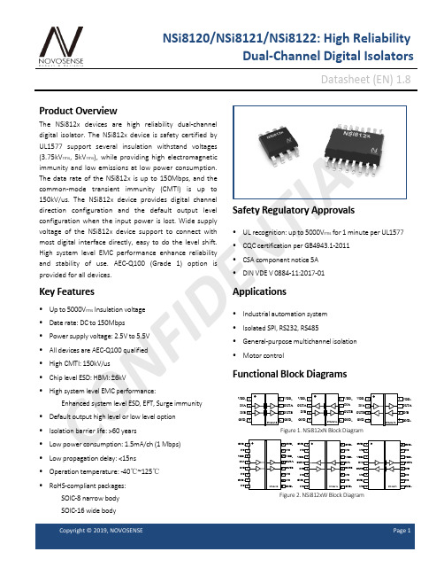
C O NF ID EN T IA LNSi8120/NSi8121/NSi8122: High ReliabilityDual-Channel Digital IsolatorsDatasheet (EN) 1.8Product OverviewThe NSi812x devices are high reliability dual-channel digital isolator. The NSi812x device is safety certified by UL1577 support several insulation withstand voltages (3.75kV rms , 5kV rms ), while providing high electromagnetic immunity and low emissions at low power consumption. The data rate of the NSi812x is up to 150Mbps, and the common-mode transient immunity (CMTI) is up to 150kV/us. The NSi812x device provides digital channel direction configuration and the default output level configuration when the input power is lost. Wide supply voltage of the NSi812x device support to connect with most digital interface directly, easy to do the level shift. High system level EMC performance enhance reliability and stability of use. AEC-Q100 (Grade 1) option is provided for all devices.Key Features• Up to 5000V rms Insulation voltage• Date rate: DC to 150Mbps• Power supply voltage: 2.5V to 5.5V • All devices are AEC-Q100 qualified • High CMTI: 150kV/us • Chip level ESD: HBM: ±6kV• High system level EMC performance:Enhanced system level ESD, EFT, Surge immunity• Default output high level or low level option • Isolation barrier life: >60 years• Low power consumption: 1.5mA/ch (1 Mbps) • Low propagation delay: <15ns • Operation temperature: -40℃~125℃ • RoHS-compliant packages:SOIC-8 narrow body SOIC-16 wide bodySafety Regulatory Approvals• UL recognition: up to 5000V rms for 1 minute per UL1577• CQC certification per GB4943.1-2011• CSA component notice 5A • DIN VDE V 0884-11:2017-01Applications• Industrial automation system • Isolated SPI, RS232, RS485• General-purpose multichannel isolation • Motor controlFunctional Block DiagramsC O NF ID EN T IA LIndex1.0 ABSOLUTE MAXIMUM RATINGS .............................................................................................................................. 3 2.0 SPECIFICATIONS ........................................................................................................................................................... 3 2.1. E LECTRICAL CHARACTERISTICS .................................................................................................................................................. 3 2.2. TYPICAL PERFORMANCE CHARACTERISTICS ........................................................................................................................... 7 2.3. P ARAMETER M EASUREMENT I NFORMATION . (8)3.0 HIGH VOLTAGE FEATURE DESCRIPTION (9)3.1. INSULATION AND SAFETY RELATED SPECIFICATIONS (9)3.2. DIN VDE V 0884-11(VDE V 0884-11):2017-01 INSULATION CHARATERISTICS ....................................................................... 9 3.3. R EGULATORY INFORMATION ................................................................................................................................................... 11 4.0 FUNCTION DESCRIPTION ..........................................................................................................................................11 5.0 APPLICATION NOTE ................................................................................................................................................... 12 5.1. PCB L AYOUT ...................................................................................................................................................................... 12 5.2. H IGH SPEED PERFORMANCE ................................................................................................................................................... 12 5.3. T YPICAL S UPPLY C URRENT E QUATIONS ..................................................................................................................................... 13 6.0 PACKAGE INFORMATION ......................................................................................................................................... 13 7.0 TAPE AND REEL INFORMATION ............................................................................................................................. 17 8.0 ORDER INFORMATION .............................................................................................................................................. 20 9.0 REVISION HISTORY . (21)C O NF ID EN T IA L1.0 ABSOLUTE MAXIMUM RATINGSPower Supply Voltage VDD1, VDD2 -0.5 6.5 V Maximum Input Voltage VINA, VINB -0.4 VDD+0.41 V Maximum Output Voltage V OUTA , V OUTB -0.4 VDD+0.41 VMaximum Input/Output Pulse VoltageVINA, VINB, V OUTA , V OUTB-0.8VDD+0.8VPulse width should be less than 100ns, and the duty cycle should be less than 10%Common-Mode Transients CMTI ±150 kV/us Output currentIo -15 15mAMaximum Surge Isolation VoltageV IOSM5.3kVOperating Temperature Topr -40125 ℃Storage Temperature Tstg -40150℃Electrostatic dischargeHBM±6000VCDM±2000V1 The maximum voltage must not exceed 6.5V.2.0 SPECIFICATIONS2.1. ELECTRICAL CHARACTERISTICS(VDD1=2.5V~5.5V, VDD2=2.5V~5.5V, Ta=-40℃ to 125℃. Unless otherwise noted, Typical values are at VDD1 = 5V, VDD2 = 5V, Ta =25℃)Power on ResetVDD POR2.2 V POR threshold as during power-upVDD HYS 0.1 V POR threshold Hysteresis Input ThresholdV IT1.6 V Input Threshold at rising edge V IT_HYS 0.4 V Input Threshold Hysteresis High Level Input Voltage V IH 2 V Low Level Input Voltage V IL 0.8 V High Level Output Voltage V OH VDD-0.3 V I OH ≤ 4mA Low Level Output VoltageV OL0.3VI OL ≤ 4mAC O NF ID EN T IA LOutput Impedance R out 50 ohm Input Pull high or low CurrentI pull 8 15 uA Start Up Time after POR trbs 40 usec Common Mode Transient ImmunityCMTI±100±150kV/us(VDD1=5V± 10%, VDD2=5V± 10%, Ta=-40℃ to 125℃. Unless otherwise noted, Typical values are at VDD1 = 5V, VDD2 = 5V, Ta = 25℃)Supply currentNSi8120 I DD1(Q0) 0.58 0.87 mAAll Input 0V for NSi8120x0 Or All Input at supply for NSi8120x1 I DD2(Q0) 1.18 1.77 mA I DD1(Q1) 2.92 4.38 mA All Input at supply for NSi8120x0 Or All Input 0V for NSi8120x1I DD2(Q1) 1.241.86mAI DD1(1M) 1.71 2.56 mA All Input with 1Mbps, C L =15pFI DD2(1M)1.382.07mAI DD1(10M) 1.78 2.67 mA All Input with 10Mbps, C L =15pF I DD2(10M)3.24.8mA I DD1(100M)2.103.15 mA All Input with 100Mbps, C L =15pFI DD2(100M)21.031.5mANSi8121/ NSi8122 I DD1(Q0) 1.031.55 mA All Input 0V for NSi812xx0 Or All Input at supply for NSi812xx1 I DD2(Q0) 1.00 1.5 mA I DD1(Q1)2.203.3 mA All Input at supply for NSi812xx0Or All Input 0V for NSi812xx1 I DD2(Q1)2.133.2 mA I DD1(1M) 1.72 2.58 mA All Input with 1Mbps, C L =15pFI DD2(1M) 1.68 2.52 mA I DD1(10M) 2.62 3.93 mA All Input with 10Mbps, C L =15pFI DD2(10M) 2.71 4.06 mA I DD1(100M) 11.01 16.5 mA All Input with 100Mbps, C L = 15pF I DD2(100M)12.8 19.2 mA Data RateDR 0 150 MbpsC O NF ID EN T IA LPropagation Delayt PLH 5 8.20 15 ns See Figure 2.7 , C L = 15pF t PHL 5 10.56 15 ns See Figure 2.7, C L = 15pF Pulse Width Distortion |t PHL – t PLH | PWD5.0nsSee Figure 2.7 , C L = 15pFRising Time t r 5.0 ns See Figure 2.7 , C L = 15pF Falling Timet f 5.0 ns See Figure 2.7 , C L = 15pFPeak Eye Diagram Jitter t JIT (PK) 350 ps Channel-to-Channel Delay Skewt SK (c2c) 2.5 nsPart-to-Part Delay Skewt SK (p2p)5.0ns(VDD1=3.3V± 10%, VDD2=3.3V± 10%, Ta=-40℃ to 125℃. Unless otherwise noted, Typical values are at VDD1 = 3.3V, VDD2 = 3.3V, Ta =25℃)Supply currentNSi8120 I DD1(Q0) 0.550.83mA All Input 0V for NSi8120x0 Or All Input at supply for NSi8120x1 I DD2(Q0) 1.12 1.68 mA I DD1(Q1) 2.87 4.3 mA All Input at supply for NSi8120x0 Or All Input 0V for NSi8120x1 I DD2(Q1)1.18 1.77mA I DD1(1M)1.72.55mA All Input with 1Mbps, C L = 15pFI DD2(1M)1.271.91 mA I DD1(10M) 1.732.6 mA All Input with 10Mbps, C L = 15pF I DD2(10M)2.413.6 mA I DD1(100M) 2.05 3.08 mA All Input with 100Mbps, C L = 15pF I DD2(100M)14.0521.08mANSi8121/ NSi8122 I DD1(Q0) 0.98 1.47 mA All Input 0V for NSi812xx0 Or All Input at supply for NSi812xx1 I DD2(Q0) 0.95 1.43 mA I DD1(Q1) 2.14 3.21 mA All Input at supply for NSi812xx0 Or All Input 0V for NSi812xx1 I DD2(Q1) 2.08 3.12 mA I DD1(1M) 1.63 2.45 mA All Input with 1Mbps, C L = 15pFI DD2(1M) 1.59 2.39 mA I (10M)2.223.33mAAll Input with 10Mbps,C O NF I D EN T IA LI DD2(10M) 2.25 3.38 mA C L = 15pFI DD1(100M) 7.57 11.36 mA All Input with 100Mbps, C L = 15pF I DD2(100M)8.5 12.75 mA Data RateDR 0 150 Mbps Minimum Pulse Width PW 5.0 nsPropagation Delayt PLH 5 9.20 15 ns See Figure 2.7 , C L = 15pF t PHL5 10.40 15 ns See Figure 2.7, C L = 15pF Pulse Width Distortion |t PHL – t PLH | PWD5.0nsSee Figure 2.7 , C L = 15pFRising Time t r 5.0 ns See Figure 2.7 , C L = 15pF Falling Timet f5.0 nsSee Figure 2.7 , C L = 15pFPeak Eye Diagram Jitter t JIT (PK) 350psChannel-to-Channel Delay Skewt SK (c2c)2.5nsPart-to-Part Delay Skew t SK (p2p)5.0ns(VDD1=2.5V± 10%, VDD2=2.5V± 10%, Ta=-40℃ to 125℃. Unless otherwise noted, Typical values are at VDD1 = 2.5V, VDD2 = 2.5V, Ta =25℃)Supply currentNSi8120I DD1(Q0) 0.53 0.8 mA All Input 0V for NSi8120x0 Or All Input at supply for NSi8120x1 I DD2(Q0) 1.11.65 mA I DD1(Q1)2.85 4.28 mA All Input at supply for NSi8120x0 Or All Input 0V for NSi8120x1 I DD2(Q1)1.15 1.73 mA I DD1(1M) 1.632.45 mA All Input with 1Mbps, C L = 15pFI DD2(1M) 1.21 1.82 mA I DD1(10M) 1.68 2.52 mA All Input with 10Mbps, C L = 15pFI DD2(10M) 2.05 3.08 mA I DD1(100M) 1.95 2.93 mA All Input with 100Mbps, C L = 15pFI DD2(100M)10.415.6mANSi8121/ NSi8122I DD1(Q0) 0.96 1.44 mA All Input 0V for NSi812xx0 Or All Input at supply for NSi812xx1I (Q0)0.931.395mAF ID EN T IA LI DD1(Q1) 2.11 3.165 mA All Input at supply for NSi812xx0Or All Input 0V for NSi812xx1 I DD2(Q1) 2.05 3.075 mA I DD1(1M) 1.58 2.37 mA All Input with 1Mbps, C L = 15pFI DD2(1M) 1.54 2.31 mA I DD1(10M) 2.02 3.03 mA All Input with 10Mbps, C L = 15pFI DD2(10M) 2.04 3.06 mA I DD1(100M) 6.03 9.045 mA All Input with 100Mbps, C L = 15pF I DD2(100M)6 9 mAData RateDR 0 150 Mbps Minimum Pulse Width PW 5.0 nsPropagation Delayt PLH 5 10 15 nsSee Figure 2.7 , C L = 15pF t PHL5 10 15nsSee Figure 2.7, C L = 15pFPulse Width Distortion |t PHL – t PLH | PWD5.0nsSee Figure 2.7 , C L = 15pFRising Time t r5.0ns See Figure 2.7 , C L = 15pF Falling Timet f5.0 ns See Figure 2.7 , C L = 15pFPeak Eye Diagram Jitter t JIT (PK)350ps Channel-to-Channel Delay Skewt SK (c2c)2.5ns Part-to-Part Delay Skew t SK (p2p)5.0ns2.2. TYPICAL PERFORMANCE CHARACTERISTICSFigure 2.1 NSi8120 VDD1 Supply Current vs Data Rate Figure 2.2 NSi8120 VDD2 Supply Current vs Data RateC OE2.3. PARAMETER MEASUREMENT INFORMATIONC LFigure 2.7 Switching Characteristics Test Circuit and WaveformFigure 2.8 Common-Mode Transient Immunity Test CircuitC O NF ID EN T IA L3.0 HIGH VOLTAGE FEATURE DESCRIPTION3.1. INSULATION AND SAFETY RELATED SPECIFICATIONSMinimum External Air Gap (Clearance)L(I01) 4.0 8.0 mm Shortest terminal-to-terminal distance through air Minimum External Tracking (Creepage)L(I02)4.08.0mmShortest terminal-to-terminal distance across the package surfaceMinimum internal gap DTI 20 um Distance through insulationTrackingResistance(Comparative Tracking Index) CTI>400VDIN EN 60112 (VDE 0303-11); IEC 60112Material GroupⅡ3.2. DIN VDE V 0884-11(VDE V 0884-11):2017-01 INSULATION CHARATERISTICSSOIC-8 SOIC-16 Installation Classification per DIN VDE 0110For Rated Mains Voltage ≤ 150V rms Ⅰto Ⅳ Ⅰto Ⅳ For Rated Mains Voltage ≤ 300V rms Ⅰto Ⅲ Ⅰto Ⅳ For Rated Mains Voltage ≤ 400V rms Ⅰto Ⅲ Ⅰto Ⅳ Climatic Classification10/105/2110/105/21 Pollution Degree per DIN VDE 0110, Table 122Maximum repetitive isolation voltageVIORM 565 849 Vpeak Input to Output Test Voltage, Method B1V IORM × 1.5 = V pd (m) , 100%production test, t ini = t m = 1 sec, partial discharge < 5 pCV pd (m)8471273VpeakInput to Output Test Voltage, Method AAfter Environmental Tests Subgroup 1V IORM × 1.2= V pd (m) , t ini = 60 sec, t m = 10 sec, partial V pd (m)6781018VpeakC O N T IA LAfter Input and /or Safety Test Subgroup 2 and Subgroup 3 V IORM × 1.2= V pd (m) , t ini = 60 sec, t m = 10 sec, partialdischarge < 5 pC V pd (m)6781018VpeakMaximum transient isolation voltage t = 60 sec VIOTM 5300 7000 Vpeak Maximum Surge Isolation VoltageTest method per IEC60065,1.2/50uswaveform, VTEST=VIOSM×1.3VIOSM53845384VpeakIsolation resistance VIO =500V RIO >109 >109 Ω Isolation capacitance f = 1MHzCIO 0.6 0.6pFInput capacitanceCI22pF Total Power Dissipation at 25℃Ps1499 mW Safety input, output, or supply currentθJA = 140 °C/W, V I = 5.5 V, T J = 150 °C, T A = 25 °C Is160mAθJA = 84 °C/W, V I = 5.5 V, T J = 150 °C, T A = 25 °C237 mA Case TemperatureTs150150℃Figure 3.2 NSi8120W/NSi8121W/NSi8122W Thermal Derating Curve, Dependence of Safety Limiting Values with Case Temperature per DIN VDE V 0884-11C O NF ID EN T IA L3.3. REGULATORY INFORMATIONThe NSi8120N/NSi8121N/NSi8122N are approved by the organizations listed in table.UL 1577 Component Recognition Program 1Approved under CSA ComponentAcceptance Notice 5ADIN VDE V 0884-11:2017-012Certified by CQC11-471543-2012 GB4943.1-2011Single Protection, 3750V rms Isolation voltageSingle Protection, 3750V rms IsolationvoltageBasic Insulation 565Vpeak, V IOSM =5384VpeakBasic insulation at 400V rms (565Vpeak)File (E500602)File (E500602)File (5024579-4880-0001)File (pending)1 In accordance with UL 1577, each NSi8120N/NSi8121N/NSi8122N is proof tested by applying an insulation test voltage ≥ 4500 Vrms for 1 sec.2 In accordance with DIN VDE V 0884-11, each NSi8120N/NSi8121N/NSi8122N is proof tested by applying an insulation test voltage ≥ 847 V peak for 1 sec(partial discharge detection limit = 5 pC). The * marking branded on the component designates DIN VDE V 0884-11 approval.The NSi8120W/NSi8121W/NSi8122W are approved by the organizations listed in table.UL 1577 Component Recognition Program 1Approved under CSAComponent Acceptance Notice5ADIN VDE V 0884-11(VDE V 0884-11):2017-012 Certified by CQC11-471543-2012 GB4943.1-2011Single Protection, 5000V rms Isolation voltageSingle Protection, 5000V rmsIsolation voltageBasic Insulation 849Vpeak, V IOSM =5384Vpeak Basic insulation at 800V rms (1131Vpeak) Reinforced insulation at 400V rms (565Vpeak)File (E500602)File (E500602)File (5024579-4880-0001)File (pending)1 In accordance with UL 1577, each NSi8120W/NSi8121W/NSi8122W is proof tested by applying an insulation test voltage ≥ 6000 V rms for 1 sec.2 In accordance with DIN VDE V 0884-11, each NSi8120W/NSi8121W/NSi8122W is proof tested by applying an insulation test voltage ≥ 1273 V peak for 1 sec(partial discharge detection limit = 5 pC). The * marking branded on the component designates DIN VDE V 0884-11 approval.4.0 FUNCTION DESCRIPTIONThe NSi812x is a Dual-channel digital isolator based on a capacitive isolation barrier technique. The digital signal is modulated with RF carrier generated by the internal oscillator at the Transmitter side. Then it is transferred through the capacitive isolation barrier and demodulated at the Receiver side.The NSi812x devices are high reliability dual-channel digital isolator with AEC-Q100 qualified. The NSi812x device is safety certified by UL1577 support several insulation withstand voltages (3.75kV rms , 5kV rms ), while providing high electromagnetic immunity and low emissions at low power consumption. The data rate of the NSi812x is up to 150Mbps, and the common-mode transient immunity (CMTI) is up to 150kV/us. The NSi812x device provides digital channel direction configuration and the default output level configuration when the input power is lost. Wide supply voltage of the NSi812x device support to connect with most digital interface directly, easy to do the level shift. High system level EMC performance enhance reliability and stability of use.The NSi812x has a default output status when VDDIN is unready and VDDOUT is ready as shown in Table 4.1, which helps for diagnosis when power is missing at the transmitter side. The output B follows the same status with the input A within 1us after powering up.C O NF ID EN T IA LCopyright © 2019, NOVOSENSEPage 12 Table 4.1 Output status vs. power statusH Ready Ready H Normal operation.L Ready Ready L XUnreadyReadyL HThe output follows the same status with the input within 60us after input side VDD1 is powered on.X Ready Unready XThe output follows the same status with the input within 60us after output side VDD2 is powered on.5.0 APPLICATION NOTE5.1. PCB LAYOUTThe NSi812x requires a 0.1 µF bypass capacitor between VDD1 and GND1, VDD2 and GND2. The capacitor should beplaced as close as possible to the package. Figure 5.1 to Figure 5.4 show the recommended PCB layout, make sure the space under the chip should keep free from planes, traces, pads and via. To enhance the robustness of a design, the user may also include resistors (50–300 Ω ) in series with the inputs and outputs if the system is excessively noisy. The series resistors also improve the system reliability such as latch-up immunity.The typical output impedance of an isolator driver channel is approximately 50 Ω, ±40%. When driving loads where transmission line effects will be a factor, output pins should be appropriately terminated with controlled impedance PCB traces.Figure5.1 Recommended PCB Layout — Top Layer Figure5.2 Recommended PCB Layout — Bottom LayerFigure5.3 Recommended PCB Layout — Top Layer Figure5.4 Recommended PCB Layout — Bottom Layer5.2. HIGH SPEED PERFORMANCEFigure 5.5 shows the eye diagram of NSi812x at 200Mbps data rate output. The result shows a typical measurement on the NSi812x with 350ps p-p jitter.C O NF ID EN T IA LFigure5.5 NSi812x Eye Diagram5.3. TYPICAL SUPPLY CURRENT EQUATIONSThe typical supply current of NSi812x can be calculated using below equations. I DD1 and I DD2 are typical supply currents measured in mA, f is data rate measured in Mbps, C L is the capacitive load measured in pFNSi8120:I DD1 = 0.19 *a1+1.45*b1+0.82*c1. I DD2 = 1.36+ VDD1*f* C L *c1*10-9When a1 is the channel number of low input at side 1, b1 is the channel number of high input at side 1, c1 is the channel number of switch signal input at side 1.NSi8121/ NSi8122:I DD1 = 0.87 +1.26*b1+0.63*c1+ VDD1*f* C L *c2*10-9I DD2 = 0.87 +1.26*b2+0.63*c2+ VDD1*f* C L *c1*10-9When b1 is the channel number of high input at side 1, c1 is the channel number of switch signal input at side 1, b2 is the channel number of high input at side 2, c2 is the channel number of switch signal input at side 2.6.0 PACKAGE INFORMATIONVDD GND 22VDD INA GND 2VDD 2Figure 6.1 NSi8120N Package Figure 6.2 NSi8121N PackageC O NF ID EN T IA LVDD INBGND 22Figure 6.3 NSi8122N PackageFigure 6.4 SOIC8 Package Shape and Dimension in millimeters (inches)Table6.1 NSi8120N/ NSi8121N/ NSi8122N Pin Configuration and DescriptionNSi8121N PIN NO.NSi8122N PIN NO.SYMBOL FUNCTION1 1 1 VDD1 Power Supply for Isolator Side 12 7 2 INA Logic Input A3 3 6 INB Logic Input B4 4 4 GND1 Ground 1, the ground reference for Isolator Side 15 5 5 GND2 Ground 2, the ground reference for Isolator Side 26 6 3 OUTB Logic Output B7 2 7 OUTA Logic Output A888VDD2Power Supply for Isolator Side 2C O NFVDD GND GND 2VDD 2GND 2GND NC NCNC VDD GND GND 2VDD 22GND NC NC NCFigure 6.5 NSi8120W Package Figure 6.6 NSi8121W PackageVDD INB GND GND 2VDD 2GND 2GND NC NC NCFigure 6.7 NSi8122W PackageFigure 6.8 WB SOIC16 Package Shape and Dimension in millimeters and (inches)C O NF ID EN T IA LTable 6.2 NSi8120W/ NSi8121W/ NSi8122W Pin Configuration and Description1 1 1 GND1 Ground 1, the ground reference for Isolator Side 12 2 2 NC No Connection.3 3 3 VDD1 Power Supply for Isolator Side 14 13 4 INA Logic Input A5 5 12 INB Logic Input B6 6 6 NC No Connection.7 7 7 GND1 Ground 1, the ground reference for Isolator Side 18 8 8 NC No Connection. 9 9 9 GND2 Ground 2, the ground reference for Isolator Side 210 10 10 NC No Connection. 11 11 11 NC No Connection. 12 12 5OUTB Logic Output A 13 4 13OUTALogic Output B 14 14 14 VDD2 Power Supply for Isolator Side 215 15 15 NC No Connection.161616GND2Ground 2, the ground reference for Isolator Side 27.0TAPE AND REEL INFORMATIONLAITNEDIFNOCC O NF ID EN T IA LFigure 7.1 Tape and Reel Information of SOIC8LAITNEDIFNOCFigure 7.2 Tape and Reel Information of WB SOIC16NF ID EN T IA L8.0 ORDER INFORMATIONNSi8120N0 3.75 2 0 150 Low -40 to 125℃ NO SOIC8 NSi8120N1 3.75 2 0 150 High -40 to 125℃ NO SOIC8 NSi8121N0 3.75 1 1 150 Low -40 to 125℃ NO SOIC8 NSi8121N1 3.75 1 1 150 High -40 to 125℃ NO SOIC8 NSi8122N0 3.75 1 1 150 Low -40 to 125℃ NO SOIC8 NSi8122N1 3.75 1 1 150 High -40 to 125℃ NO SOIC8 NSi8120W0 5 2 0 150 Low -40 to 125℃ NO WB SOIC16 NSi8120W1 5 2 0 150 High -40 to 125℃ NO WB SOIC16 NSi8121W0 5 1 1 150 Low -40 to 125℃ NO WB SOIC16 NSi8121W1 5 1 1 150 High -40 to 125℃ NO WB SOIC16 NSi8122W0 5 1 1 150 Low -40 to 125℃ NO WB SOIC16 NSi8122W1 5 1 1 150 High -40 to 125℃ NO WB SOIC16 NSi8120N0Q 3.75 2 0 150 Low -40 to 125℃ YES SOIC8 NSi8120N1Q 3.75 2 0 150 High -40 to 125℃ YES SOIC8 NSi8121N0Q 3.75 1 1 150 Low -40 to 125℃ YES SOIC8 NSi8121N1Q 3.75 1 1 150 High -40 to 125℃ YES SOIC8 NSi8122N0Q 3.75 1 1 150 Low -40 to 125℃ YES SOIC8 NSi8122N1Q 3.75 1 1 150 High -40 to 125℃ YES SOIC8 NSi8120W0Q 5 2 0 150 Low -40 to 125℃ YES WB SOIC16 NSi8120W1Q 5 2 0 150 High -40 to 125℃ YES WB SOIC16 NSi8121W0Q 5 1 1 150 Low -40 to 125℃ YES WB SOIC16 NSi8121W1Q 5 1 1 150 High -40 to 125℃ YES WB SOIC16 NSi8122W0Q 5 1 1 150 Low -40 to 125℃ YES WB SOIC16 NSi8122W1Q 5 1 1 150 High -40 to 125℃YES WB SOIC16 NOTE: All packages are RoHS-compliant with peak reflow temperatures of 260 °C according to the JEDEC industry standard classifications and peak solder temperatures. All devices are AEC-Q100 qualified.Part Number Rule:NSi(81)(2)(1)(N)(1)(Q)C O NF ID EN T IA LNSi8120/NSi8121/NSi81229.0 REVISION HISTORY1.0 Original2017/11/15 1.1 Change to Ordering information2018/3/26 1.2 Add maximum operation current specification. 2018/6/20 1.3 Change block diagram 2018/7/28 1.4 Correct Table 6.2 Pin No.2018/8/20 1.5 Add specification “Input Pull high or low Current” 2018/9/10 1.6 Add “Maximum Input/Output Pulse Voltage” 2018/10/91.7 Change to Ordering information 2018/12/20 1.8 Change Certification Information2019/06/17。
JDSU MTS T-BERD 8000平台光谱分析器模块说明书

MTS/T-BERD 8000 PlatformOptical Spectrum Analyzer ModulesFull-band, high-performance Optical Spectrum Analyzers for testing optical systems and componentsTargeted at providing advanced test solutions, the OSA-150, OSA-180 and the OSA-500 are the next generation of JDSU’s DWDM analyzer modules.A new monochromator design provides ultra high optical resolution, and outstanding wavelength accuracy in a small and rugged OSA module, offering the best field solution for testing DWDM and CWDM networks during installation, maintenance and trouble shooting.The JDSU OSA modules differentiate by the optical measurement resolution and are graded into three classes:The OSA-150 is JDSU’s basic OSA with an optical resolution of 100 pm to measure CWDM and • DWDM networks with moderate channel spacing of 100 GHz to CWDM.The high resolution OSA-18x DWDM analyzers are suited for testing DWDM networks with • tight channel spacing down to 50GHz. In addition the OSA-181 provides a unique channel drop function to isolate single DWDM channels from the spectrum.The ultra high resolution OSA-500 and OSA-500R have an industry leading resolution band-• width of 35 pm for measurements in ultra DWDM networks with channel spacing down to 25 Hz.The OSA-500R is equipped additionally with a new technique to measure the true OSNR in ROADM systems and 40G systems.Key FeaturesI n-band capability for true OSNR measurements in •ROADM and 40G networks Ultra-high optical resolution•Industry-leading wavelength accuracy guaranteed over •instruments lifetimeFuture-proof signal analysis for data rates of 40/100G,•and next-generation modulation formatsChannel drop function for single channel isolation and •tunable filter applications.PMD test option based on fixed analyzer method.•MTS/T-BERD platformApplicationsCommissioning and•maintenance of current and next generation DWDM systemsProvisioning and maintenance •of ROADM networksInstallation and maintenance of •CWDM networks Testing of 40G and 100G •networksSpectral testing of optical •components1981Advanced optical performanceJDSU’s OSA family combines outstanding wavelength accuracy, high dynamic range and an ultra-high resolution. All instruments are equipped with an internal wavelength reference for online calibration without requiring disruption of in-progress measurements. The internal wavelength calibrator is based on a physical constant reference that guarantees unsurpassed wavelength accu-racy over the instrument’s lifetime without the need of external recalibration (JDSU patents), saving recalibration cost.One-step system qualificationOne-button auto-testing guarantees that technicians need no special training to carry out a DWDM test, making JDSU’s instruments suitable for both novice and expert technicians. An Auto-Test mode automatically identifies WDM channels, selects the appropriate wavelength range, and provides auto scaling and system qualification according to pre-defined parameters.Flexible measurement capabilityIn-depth analysis, featuring statistical evaluation, and automatic storage capabilities, is provided. This allows for DWDM system performance verification, including the variation of optical sys-tem parameters (wavelength, power, and OSNR) as well as a series of measurements over a defined period of time. Resulting reports are provided with average, minimum, maximum, and standard deviation values of the measured parameters over time.Powerful pass/fail link managerGraphical and tabular display formats can be selected to assist in the installation, verification, and troubleshooting of multi-channel DWDM systems. Built-in test functions deliver automatic pass/ fail evaluations based on pre-defined alarms, saving time and providing technicians with a quick and intuitive overview of the complete set of results.Measurement of signals at high data rates and new modulation formatsData rates at 10 Gbps or higher have a larger optical bandwidth than the resolution bandwidth of an OSA, and with new modulation formats like duobinary (DB), differential phase shift keying (DPSK) or quadratur phase shift keying (QPSK), the spectral shape of a signal will change from one peak to multiple peaks. Regular OSAs will no longer correctly measure the central wavelength and the total signal power of such transmission signals.JDSU OSAs are prepared for these scenarios as they have a new signal analysis for accurate mea-surement of total channel power and center wavelength of modulated signals. All results will be presented in the WDM table.40 channel DWDM systemGraphical and tabular display showing pass/fail indicators and out-of-range valuesInstrument setupPrecise and correct detection of new modulation formatsNew in-band OSNR measurement techniqueIn ROADM networks the noise floor in between optical channels is suppressed by the optical fil-ters inside the ROADMs. In systems transmitting ultra high data rates like 40G/100G at tight channel spacing of 50 GHz, the modulation bandwidth is larger than the channel bandwidth thus leading to overlapping spectra. Both effects make conventional OSNR measurement based on the IEC interpolation method unreliable.The OSA-500R is JDSUs second generation of opti-cal spectrum analyzers performing the in-bandOSNR A new optical polarization splitting (OPS) method (patent pending) is used to suppress the transmission signal and to get access to the noise value inside the optical channel for measuring the true in-band OSNR. The only viable solution for any test scenarios, whatever the ROADM filter types, data rate or modulation formats.Built-in test applicationsTest applications for optical amplifiers (EDFA) and laser sources (DFB) facilitate network compo-nent verification.Drift measurementsFor optical performance monitoring it is essential to measure the key parameters over time. The built-in drift test application provides the result of power, wavelength and OSNR over a customer definable time frame in a graphical and numerical format. Drift measurements are important in CWDM networks with uncooled laser, which have a typical wavelength of 0.1 nm/°C.PMD test optionsWith the PMD option, the OSA can measure the differential group delay (DGD) for PMD charac-terization of optical fibers and systems. The measurement is based on the fixed analyzer method (TIA/EIA FOTP-113) together with a broadband source and a variable polarizer.Channel isolation (drop) and dual-port optionsA unique channel isolation option is provided to extract a single DWDM channel from the entire spectrum for further analysis with a SONET/SDH or Ethernet analyzer at data rates up to 12.5 Gbps. The built-in tracking function provides wavelength locking to the peak of the selected chan-nel in order to avoid channel frequency drift problems during long-term measurements. The dual-port option (JDSU patents) provides simultaneous measurement of two optical signals, mea-suring the input and output of an optical amplifier at the same time, for example.Advanced analysis solutionJDSU’s OFS-100 Optical FiberTrace Software is a PC-based software application within a true Microsoft Windows environment, offering post-analysis capabilities and the generation of detailed, professional OSA reports.Offline analysis OFS-100EDFA test applicationIn-band noise measurement of optical channels passingdifferent routes in a ROADM networkDrift analysisFull-band WDM analyzerOSA-150Operating modesWDM, DriftSpectral measurement ranges Wavelength range1250 to 1650 nm Measurement samples120,000 No. of optical channels256 Wavelength calibration (1)internal, online. Wavelength accuracy (2)± 100 pm Readout resolution 1 pm Resolution bandwidth(FWHM) (2)100 pmPower measurement rangesDynamic range (3)−60 to +15 dBm Absolute accuracy(2, 4)± 0.6 dBTotal safe power+23 dBm Readout resolution0.01 dBScanning time (full band) (C-band)<5 s <1 sOptical rejection ratio (ORR) (2)at ± 25 GHz (± 0.2 nm)not specified at ± 50 GHz (± 0.4 nm)40 dBc at ± 100 GHz (± 0.8 nm)>43 dBc(1) Built-in, physical constant wavelength calibrator,needs no re-calibration(2) Typical for 1520 to 1565 nm at 18° to 28 °C(3) Max. power per channel +15 dBm(4) At −10 dBm, including PDL(5) −45 dBm to +10 dBm, at 23 °C Full band DWDM AnalyzerOSA-180 / OSA-181Operating modesWDM, Drift, DFB, LED, FPL, EDFASpectral measurement rangesWavelength range1250 to 1650 nmMeasurement samples120,000No. of optical channels256Wavelength calibration (1)internal, online.Wavelength accuracy (2)typ. ± 20 pmReadout resolution 1 pmResolution bandwidth(FWHM) (2)typ. 70 pmPower measurement rangesDynamic range (3)−65 to +23 dBmAbsolute accuracy(2, 4)typ. ± 0.5 dBLinearity (5)± 0.1 dBTotal safe power+23 dBmReadout resolution0.01 dBScanning time (full band)(C-band)<5 s<1 sOptical rejection ratio (ORR) (2)at ± 25 GHz (± 0.2 nm)typ. 35 dBcat ± 50 GHz (± 0.4 nm)typ. 45 dBcChannel drop option (OSA-181 only)Wavelength range 1300 to 1650 nmData rates up to 12.5 GbpsSpectral filter bandwidth>20 GHzInsertion loss(6)typ. <12 dBTracking mode Auto wavelength control(6) 1520 to 1620 nm at 23 °C(7) For data rates up to 10 Gbps(8) For OSNR ≤ 25 dB and PMD <25 psFor data rates of ≥ 40 Gbpswith ≥ 100 GHz ch- spacing typically ± 1 dB(9) Fast mode, independent of no of channelsHigh Perf. DWDM AnalyzerOSA-500 / OSA-500ROperating modesWDM, Drift, DFB, LED, FPL, EDFAIn-band OSNR (OSA-500R only)Spectral measurement rangesWavelength range1250 to 1650 nmMeasurement samples120,000No. of optical channels256Wavelength calibration(1)internal, online.Wavelength accuracy (2)typ. ± 10 pmReadout resolution 1 pmResolution bandwidth(FWHM) (2)typ. 35 pmPower measurement rangesDynamic range (3)−70 to +20 dBmAbsolute accuracy(2, 4)typ. ± 0.5 dBLinearity (5)± 0.1 dBTotal safe power (12)+23 dBmReadout resolution0.01 dBScanning time (full band)(C-band)<5 s<1 sOptical rejection ratio (ORR) (2, 11)at ± 25 GHz (± 0.2 nm)typ. 45 dBcat ± 50 GHz (± 0.4 nm)typ. 50 dBcIn-band OSNR (10) (OSA-500R only)I-OSNR dynamic range up to >30 dBPMD tolerance (7)up to 25 psMeasurement accuracy(8)typ. ± 0.5 dBData signals up to 100 GbpsMeasurement time(9)<2 min(10) only valid for OSA-500R(11) For OSA-500R ORR is reduced by 3 dB(12) +20 dBm for OSA-500ROSA Selection GuideA comprehensive portfolio to better match your application requirements.ApplicationTechnology CWDM DWDM DWDM UDWDM Channel drop ROADMin-band OSNR Instrument class Ch-spacing20 nm100 GHz50 GHz25 GHzBasic OSA OSA-150X X––––High resolution OSA OSA-180X X X–––OSA-181X X X–X–Ultra high resolution OSA OSA-500X X X X––OSA-500R X X X X–XGeneral specificationsDisplay modesGraph, WDM table, graph and tableOptical ports (physical contact interfaces)Input port SMOutput port (drop port OSA-181)SMOptical return loss>35 dBInterface Universal connectors/PCOptical adapters FC, SC, ST, LC, DINTemperatureOperating+5 to +50 °C / 41 to 122 °FStorage−20 to +60 °C / -4 to 140 °FWeight (module only )OSA-150/18x/500 2.2 kg / 4.6 lbsSize (module only )OSA-150/18x/50050 x 250 x 305 mm /2 x 10 x 12 inOSA modulesOrdering information for Full-band DWDM analyzersBasic OSAs2281/91.15OSA-150High-resolution OSAs2281/91.18OSA-1802281/91.22OSA-181, with channel drop 12.5GUltra-high resolution OSAs2281/91.51OSA-500, high performance DWDM OSA2281/91.55OSA-500R, high performance DWDM & ROADM OSAPMD test option (for OSA-18x/500/500R)2281/91.11PMD test kitincludes PMD evaluation SW plus2279/31OBS-55, Optical Broadband Sourceplus2271/01OVP-15, Optical Variable PolarizerApplication softwareEOFS100Optical fiber trace software for post-analysisEOFS200Optical fiber trace software for cable acceptance report generation Test & Measurement Regional Sales。