I2C总线实验(实时时钟
DS3231高精度I2C实时时钟(R

DS3231 高精度I2C 实时时钟(R
DS3231 是低成本、高精度I2C 实时时钟(RTC),具有集成的温补晶振(TCXO)和晶体。
该器件包含电池输入端,断开主电源时仍可保持精确的计时。
集成晶振提高了器件的长期精确度,并减少了生产线的元件数量。
DS3231 提供商用级和工业级温度范围,采用16 引脚300mil 的SO 封装。
RTC 保存秒、分、时、星期、日期、月和年信息。
少于31 天的月份,将自动调整月末的日期,包括闰年的修正。
时钟的工作格式可以是24 小时或带/AM/PM 指示的12 小时格式。
提供两个可设置的日历闹钟和一个可设置的方波输出。
地址与数据通过I²C 双向总线串行传输。
精密的、经过温度补偿的电压基准和比较器电路用来监视VCC 状态,检测电源故障,提供复位输出,并在必要时自动切换到备份电源。
另外,
/RST 监视引脚可以作为产生µP 复位的手动输入。
关键特性
0°C至+40°C范围内精度为±2ppm
-40°C至+85°C范围内精度为±3.5ppm
为连续计时提供电池备份输入。
基于I2C总线的实时时钟芯片设计

基于I2C总线的实时时钟芯片设计
龚光松
【期刊名称】《软件导刊》
【年(卷),期】2012(011)004
【摘要】基于I2C总线的实时时钟芯片X1202具有接口简单、记时功能齐全等优点.介绍了X1202芯片的工作原理、编程方法及应用.
【总页数】4页(P97-100)
【作者】龚光松
【作者单位】咸宁职业技术学院,湖北咸宁437100
【正文语种】中文
【中图分类】TP319
【相关文献】
1.基于UAF42芯片设计通用滤波器基于UAF42芯片设计通用滤波器 [J], 陈建尹
2.基于LPC1768的多功能实时时钟系统设计 [J], 徐永毅;张燕
3.基于I2C总线的超高精度实时时钟芯片PCF2129的应用 [J], 王洪武;张戟
4.基于增强51芯片W77E516和RV8803-C7实时时钟的实现方法 [J], 韩霜
5.基于STM32的可记忆高精度实时时钟系统 [J], 孙晓峰;蒋伯华;王鹏;李广恒;刘承文
因版权原因,仅展示原文概要,查看原文内容请购买。
实时时钟实验总结
实时时钟实验总结一、实验目的本实验的主要目的是了解实时时钟的原理及其应用,掌握实时时钟的使用方法,以及通过实验学习如何编写驱动程序。
二、实验原理1. 实时时钟是一种能够提供时间和日期信息的芯片,它通常由一个晶体振荡器和一组计数器组成。
2. 实时时钟可以通过I2C总线与处理器进行通信,读取或设置时间和日期信息。
3. 实现实时时钟需要编写相应的驱动程序,并将其与操作系统进行集成。
三、实验设备与材料1. 实验板:STM32F407ZET6开发板;2. 模块:DS1307实时时钟模块;3. 软件:Keil uVision5开发环境。
四、实验内容1. 硬件连接:将DS1307模块与STM32F407ZET6开发板连接,包括SDA、SCL、VCC和GND等引脚。
2. 编写驱动程序:根据DS1307模块手册编写相应的驱动程序,并将其集成到操作系统中。
3. 测试程序:编写测试程序,通过读取DS1307模块返回的时间和日期信息来验证驱动程序是否正常工作。
五、实验步骤1. 连接硬件:将DS1307模块与STM32F407ZET6开发板连接。
2. 编写驱动程序:根据DS1307模块手册编写相应的驱动程序,并将其集成到操作系统中。
3. 编写测试程序:编写测试程序,通过读取DS1307模块返回的时间和日期信息来验证驱动程序是否正常工作。
4. 下载程序:使用Keil uVision5开发环境将编写好的程序下载到STM32F407ZET6开发板上。
5. 运行测试:启动STM32F407ZET6开发板,通过串口助手等工具查看DS1307模块返回的时间和日期信息,验证驱动程序是否正常工作。
六、实验结果经过测试,实时时钟模块能够正确返回当前时间和日期信息,并且能够根据需要进行设置和调整。
七、实验总结本次实验通过对实时时钟原理的学习以及编写驱动程序和测试程序的练习,加深了对嵌入式系统中硬件与软件协同工作的理解。
同时也掌握了一些基本的嵌入式系统开发技能,如硬件连接、驱动编写、调试等。
带看门狗、实时时钟的I2C总线铁电存储器FM31256

带看门狗、实时时钟的I2C总线铁电存储器FM31256摘要 FM31256是⼀种基于I2C总线、采⽤铁电体技术的多功能存储芯⽚。
除了⾮易失存储器外,该器件还具有实时时钟、低电压复位、看门狗计数器、⾮易失性事件计数器、可锁定的串⾏数字标识等多种功能。
⽂章主要介绍了FM31256的基本功能、原理,并结合实例给出了其在电磁铸轧电源控制装置中的具体应⽤⽅法。
关键词 I2C总线铁电体技术 RTC MSP430F FM31256是由Ramtron公司推出的新⼀代多功能系统监控和⾮易失性铁电存储芯⽚。
与其他⾮易失性存储器⽐较,它具有如下优点:读/写速度快,没有写等待时间;功耗低,静态电流⼩于1 mA,写⼊电流⼩于150mA;擦写使⽤寿命长,芯⽚的擦写次数为100亿次,⽐⼀般的EEPROM存储器⾼10万倍,即使每秒读/写30次,也能⽤10年;读/写的⽆限性,芯⽚擦写次数超过100亿次后,还能和SRAM⼀样读/写。
铁电存储器(FRAM)的核⼼技术是铁电晶体材料。
这⼀特殊材料使铁电存储器同时拥有随机存取存储器(RAM)和⾮易失性存储的特性。
本⽂介绍了FM31256的主要功能,并具体给出了基于嵌⼊式C语⾔编写的存储器读/写程序。
1 FM31256的基本结构及原理 FM31256由256 KB存储器和处理器配套电路(processor companion)两部分组成。
与⼀般的采⽤备份电池保存数据不同,FM31256是真正意义上的⾮易失(truly nonvolatile)存储器,并且⽤户可以选择对不同的存储区域以软件⽅式进⾏写保护。
FM31256器件将⾮易失FRAM与实时时钟(RTC)、处理器监控器、⾮易失性事件计数器、可编程可锁定的64位ID号和通⽤⽐较器相结合。
其中,通⽤⽐较器可提前在电源故障中断(NMI)时发挥作⽤或实现其他⽤途。
采⽤先进的0.35µm制造⼯艺,这些功能通过⼀个通⽤接⼝嵌⼊到14个引脚的SOIC封装中,从⽽取代系统板上的多个元件。
实时时钟模块(I2C总线)PT7C4311说明书

Real-time Clock Module (I2C Bus)Features→→→→→→→→→→→→→→→→→。
DescriptionFunction BlockNotes:1. No purposely added lead. Fully EU Directive 2002/95/EC (RoHS), 2011/65/EU (RoHS 2) & 2015/863/EU (RoHS 3) compliant.2. See https:///quality/lead-free/ for more information about Diodes Incorporated’s definitions of Halogen - and Antimony-free, "Green" and Lead-free.3. Halogen- and Antimony-free "Green” products are defined as those which contain <900ppm bromine, <900ppm chlorine (<1500ppm total Br + Cl) and <1000ppmSOMaximum RatingsDC Electrical Characteristics(Unless otherwise specified, V= 1.5 ~ 5.5 V, T = -40 °C to +85 °C.)1.After switchover (V SO), V BAT (min) can be2.0V for crystal with R S=40kΩ.2.Switch-over and deselect point.3.Valid for Ambient Operating Temperature: T A = -40 to 85°C; V CC = 2.0 to 5.5V (except where noted). VCC fall time should not exceed 5mV/μs.4.All voltages referenced to GND.5.In 3.3V application, if initial battery voltage is ≥ 3.4V, it may be necessary to reduce battery voltage (i.e., through wave soldering thebattery) in order to avoid inadvertent switchover/reselection for VCC – 10% operation.6.For rechargeable backup, V BAT (max) may be considered to be V CC.AC Electrical CharacteristicsTiming DiagramRecommended Layout for Crystal1212 the equation as below:Cpar + [(C1+C G)*(C2+C D)]/ [(C1+C G)+(C2+C D)] =C LCpar is all parasitical capacitor between X1 and X2.C L is crystal’s load capacitance.Note: The crystal, traces and crystal input pinsshould be isolated from RF generating signals.Function DescriptionOverview of Functions1.Clock function2.Interface with CPU3.Oscillator enable/disable4.Calibration functionRegisters*1. PT7C4311 uses 6 bits for address. That is if write data to 41H, the data will be written to 01H address register.*2. Stop bit. When this bit is set to 1, oscillator and time count chain are both stopped.*3. CEB: Century Enable Bit. CB: Century Bit.*4. Control FT/OUT pin output DC level when 512Hz square wave is disabled.*5. Frequency Test. 512Hz square wave output is enabled at FT/OUT pin, which is using for frequency test.*6. Sign Bit. “1” indicates positive calibration; “0”indicates negative calibration.*7. Using for modifying count frequency. If 20ppm is wanted to slow down the count frequency, 10 (01010) should be loaded. *8. Initialize the control and status register to 10000000 if calibration function is not required.Clock calibrationCalibration:3.Time Counter∙∙∙* Note 2: Do not care.* Note 3: Century Enable Bit and Century Bit.4.Days of the week Counter5.Calendar Counter∙∙Communication1.I2C Bus Interfacea)Overview of I2C-BUSb)System ConfigurationFig.1 System configurationc)Starting and Stopping I2C Bus Communications∙∙∙d)Data Transfers and Acknowledge Responses during I2C-BUS Communication∙Data transfers*Note: with caution that if the SDA data is changed while the SCL line is at high level, it will be treated as a START, RESTART, or STOP condition.Fig.2 Starting and stopping on I2C busData acknowledge response (ACK signal)e)Slave Address2.I2C Bus’s Basic Transfer FormatSCL from Master1289SDA from transmitter(sending side)SDA from receiver(receiving side)Release SDALow activeACK signala)Write via I2C busb)Read via I2C bus∙Standard read∙Simplified readNote:1.The above steps are an example of transfers of one or two bytes only. There is no limit to the number of bytes transferredduring actual communications.2.49H, 4AH are used as test mode address. Customer should not use the addresses.Part MarkingW Package ZE PackagePackaging Mechanical 8- SOIC (W)8- TDFN (ZE)Ordering Information1.No purposely added lead. Fully EU Directive 2002/95/EC (RoHS), 2011/65/EU (RoHS 2) & 2015/863/EU (RoHS 3) compliant.2.See https:///quality/lead-free/ for more information about Diodes Incorporated’s definitions of Halogen- and Antimony-free, "Green" andLead-free.3.Halogen- and Antimony-free "Green” produ cts are defined as those which contain <900ppm bromine, <900ppm chlorine (<1500ppm total Br + Cl) and<1000ppm antimony compounds.4. E = Pb-free and Green5.X suffix = Tape/ReelIMPORTANT NOTICEDIODES INCORPORATED MAKES NO WARRANTY OF ANY KIND, EXPRESS OR IMPLIED, WITH REGARDS TO THIS DOCUMENT, INCLUDING, BUT NOT LIMITED TO, THE IMPLIED WARRANTIES OF MERCHANTABILITY AND FITNESS FOR A PARTICULAR PURPOSE (AND THEIR EQUIVALENTS UNDER THE LAWS OF ANY JURISDICTION).Diodes Incorporated and its subsidiaries reserve the right to make modifications, enhancements, improvements, corrections or other changes without further notice tothis document and any product described herein. Diodes Incorporated does not assume any liability arising out of the application or use of this document or any product described herein; neither does Diodes Incorporated convey any license under its patent or trademark rights, nor the rights of others. Any Customer or user of this document or products described herein in such applications shall assume all risks of such use and will agree to hold Diodes Incorporated and all the companies whose products are represented on Diodes Incorporated website, harmless against all damages.Diodes Incorporated does not warrant or accept any liability whatsoever in respect of any products purchased through unauthorized sales channel.Should Customers purchase or use Diodes Incorporated products for any unintended or unauthorized application, Customers shall indemnify and hold Diodes Incorporated and its representatives harmless against all claims, damages, expenses, and attorney fees arising out of, directly or indirectly, any claim of personal injuryor death associated with such unintended or unauthorized application.Products described herein may be covered by one or more United States, international or foreign patents pending. Product names and markings noted herein may also be covered by one or more United States, international or foreign trademarks.This document is written in English but may be translated into multiple languages for reference. Only the English version of this document is the final and determinative format released by Diodes Incorporated.LIFE SUPPORTDiodes Incorporated products are specifically not authorized for use as critical components in life support devices or systems without the express written approval of the Chief Executive Officer of Diodes Incorporated. As used herein:A. Life support devices or systems are devices or systems which:1. are intended to implant into the body, or2. support or sustain life and whose failure to perform when properly used in accordance with instructions for use provided in the labeling can be reasonably expected to result in significant injury to the user.B. A critical component is any component in a life support device or system whose failure to perform can be reasonably expected to cause thefailure of the life support device or to affect its safety or effectiveness.Customers represent that they have all necessary expertise in the safety and regulatory ramifications of their life support devices or systems, and acknowledge andagree that they are solely responsible for all legal, regulatory and safety-related requirements concerning their products and any use of Diodes Incorporated products in such safety-critical, life support devices or systems, notwithstanding any devices- or systems-related information or support that may be provided by Diodes Incorporated. Further, Customers must fully indemnify Diodes Incorporated and its representatives against any damages arising out of the use of Diodes Incorporated products in such safety-critical, life support devices or systems.Copyright © 2020, Diodes Incorporated。
综合实验四 IIC总线实验

图8-6流程图C51程序:#include<reg51.h>sbit SDA=P3^7;sbit SCL=P3^6;sbit reset=P3^3;//函数声明unsigned char LED_seg[10]={0xc0,0xf9,0xa4,0xb0,0x99,0x92,0x82,0xf8,0x80,0x90}; //共阳unsigned char LED_bit[4]={0x01,0x02,0x04,0x08}; //数码unsigned LED_buf[6]={0,0,0,0}; //数码unsigned char i2c_read(unsigned char);void i2c_write(unsigned char,unsigned char);void i2c_send8bit(unsigned char);unsigned char i2c_receive8bit(void);void i2c_start(void);void i2c_stop(void);bit i2c_ack(void);void delay(unsigned int j) //延时{while(j--);}void convert(unsigned long n){unsigned char i=0;while(i<4){LED_buf[i]=(unsigned char)(n%10);n=n/10;i++;}}//======================================================= void main(void){unsigned char dd,i,j;dd=i2c_read(0x00);dd++;j=dd;i2c_write(0x00,dd);while(1){convert(dd);for(i=0;i<2;i++){P0=LED_seg[LED_buf[i]];P1=LED_bit[i];delay(500);}if(reset==0){dd=0x00;i2c_write(0x00,dd);//写入0x00}}}/*======================================================= i2c_write(地址,数据),写一个字节=======================================================*/ void i2c_write(unsigned char Address,unsigned char Data){do{i2c_start();i2c_send8bit(0xA0);}while(i2c_ack());i2c_send8bit(Address);i2c_ack();i2c_send8bit(Data);i2c_ack();i2c_stop();}/*=======================================================i2c_read(地址,数据),读一个字节=======================================================*/ unsigned char i2c_read(unsigned char Address){unsigned char c;do{i2c_start();i2c_send8bit(0xA0);}while(i2c_ack()); //=1,表示无确认,再次发送i2c_send8bit(Address);i2c_ack();do{i2c_start();i2c_send8bit(0xA1);}while(i2c_ack());c=i2c_receive8bit();i2c_ack();i2c_stop();return(c);}//======================================================= //发送开始信号void i2c_start(void){SDA=1;SCL=1;SDA=0;SCL=0;//return;}//发送结束信号void i2c_stop(void){SCL=0;SDA=0;SCL=1;SDA=1;//return;}//发送接收确认信号bit i2c_ack(void){bit ack;SDA = 1;SCL = 1;delay(200);if(SDA==1)ack = 1;else ack = 0;SCL = 0;return(ack);}//送八位数据void i2c_send8bit(unsigned char b){unsigned char i=8;while(i--){SCL=0;SDA=(bit)(b&0x80); b<<=1;SCL=1;}SCL=0;}//i2c接收八位数据unsigned char i2c_receive8bit(void){unsigned char i=8;unsigned char dat=0;SDA=1;while(i--){dat<<=1;SCL=0;SCL=1;dat|=SDA;}SCL=0;return(dat);}四、实验仪器和设备Keil软件;A T89S52实验平台;ISP在线编程软件;五、实验结果和数据分析问题:1.说明IIC总线操作过程;2.说明24C04的操作过程。
周立功—I2C 总线实验
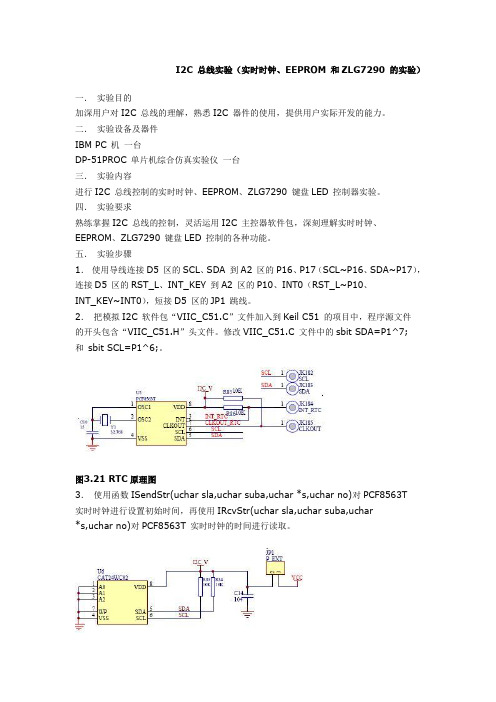
I2C 总线实验(实时时钟、EEPROM 和ZLG7290 的实验)一.实验目的加深用户对I2C 总线的理解,熟悉I2C 器件的使用,提供用户实际开发的能力。
二.实验设备及器件IBM PC 机一台DP-51PROC 单片机综合仿真实验仪一台三.实验内容进行I2C 总线控制的实时时钟、EEPROM、ZLG7290 键盘LED 控制器实验。
四.实验要求熟练掌握I2C 总线的控制,灵活运用I2C 主控器软件包,深刻理解实时时钟、EEPROM、ZLG7290 键盘LED 控制的各种功能。
五.实验步骤1.使用导线连接D5 区的SCL、SDA 到A2 区的P16、P17(SCL~P16、SDA~P17),连接D5 区的RST_L、INT_KEY 到A2 区的P10、INT0(RST_L~P10、INT_KEY~INT0),短接D5 区的JP1 跳线。
2.把模拟I2C 软件包“VIIC_C51.C”文件加入到Keil C51 的项目中,程序源文件的开头包含“VIIC_C51.H”头文件。
修改VIIC_C51.C 文件中的sbit SDA=P1^7;和sbit SCL=P1^6;。
图3.21 RTC原理图3.使用函数ISendStr(uchar sla,uchar suba,uchar *s,uchar no)对PCF8563T实时时钟进行设置初始时间,再使用IRcvStr(uchar sla,uchar suba,uchar*s,uchar no)对PCF8563T 实时时钟的时间进行读取。
EEPROM 原理图4.使用函数ISendStr(uchar sla,uchar suba,uchar *s,uchar no);对24WC02EEPROM 进行写入,再使用IRcvStr(uchar sla,uchar suba,uchar *s,uchar no);对24WC02 EEPROM 进行读取。
ZLG7290 原理图5.对ZLG7290 键盘LED 控制器的操作也同理,只是在程序开始的地方增加复位操作和程序中间增加查询是否有键按下。
HYM1307 带 56 字节 RAM 的 I2C 串行实时时钟芯片说明书
HYM1307HYM1307带56字节RAM 的I 2C 串行实时时钟芯片特点■基于32.768kHz 的石英晶体,可对秒,分,时,日,月,周以及带闰年补偿的年进行计数■带备用电池的56字节非易失性RAM ■I 2C 串行总线接口■可编程方波输出■自动掉电检测及电源切换电路■电池供电下,振荡器工作时的消耗小于500nA ■可选的工业温度范围:-40℃至+85℃■封装形式:DIP8和SOP8应用■、IC 卡水表、IC 卡煤气表■移动电话■便携仪器■传真机■电池电源产品■电视机概述HYM1307是一款低功耗、带56个字节用户非易失性SRAM (NV SRAM )、全BCD 码的时钟/日历电路。
地址和数据通过串行I 2C 总线传递。
时钟/日历提供秒、分、小时、周、日、月和年信息。
对小于31天的月,月末的日期自动进行调整,还具有闰年校正的功能。
时钟可以工作在24小时格式或带AM/PM 标志的12小时格式。
HYM1307有一个内置的电压判断电路,具有检测电源掉电功能,在电源掉电时,可自动切换到由备用电源(电池)供电。
定购信息型号工作温度范围封装类型HYM1307DIP8HYM1307Z 0℃~70℃SOP8HYM1307N DIP8HYM1307ZN-40℃~+85℃SOP8付费率电度表方框图和管脚功能方框图图1内部方框图管脚图DIP8SOP8管脚说明序号符号描述1X132.768kHz晶体引脚2X232.768kHz晶体引脚3V BAT+3V电池输入4GND地5SDA串行数据输入/输出。
SDA是I2C串行接口的输入/输出线,此引脚为漏极开路6SCL串行时钟。
SCL是I2C串行接口的时钟线,此引脚为漏极开路7SQW/OUT方波输出驱动脚,此引脚为漏极开路8V CC电源输入引脚绝对最大额定值参数名称额定值单位所有引脚到地的电压-0.5~+7.0V贮存温度-55~+125℃DIP8,10秒260℃焊接温度SOP8,10sec260推荐直流工作条件参数符号最小值典型值最大值单位注释电源电压V CC 4.5 5.0 5.5V逻辑1电压V IH 2.2V CC+0.3V逻辑0电压V IL-0.5+0.8V电池电压V BAT 2.0 3.5V直流电气特性参数符号最小值典型值最大值单位注释输入漏电流(SCL)I LI1µAI/O漏电流(SDA&SQW/OUT)I LO1µA逻辑0输出(I OL=5mA)V OL0.4V电源工作电流I CCA 1.5mA7静态电流I CCS200µA1电池电流(OSC ON);I BAT1300500nA2 SQW/OUT OFF电池电流(OSC ON);I BAT2480800nASQW/OUT ON(32kHz)电源失效电压V PF 1.216×V BAT 1.25×V BAT 1.284×V BAT V8交流电气特性参数符号最小值典型值最大值单位注释SCL时钟频率f SCL0100kHzSTOP条件和START条件t BUF 4.7µs之间总线的空闲时间START条件的保持时间t HDSTA 4.0µs3SCL低周期t LOW 4.7µsSCL高周期t HIGH 4.0µsSTART条件的建立时间t SUSTA 4.7µs数据保持时间t HDDAT0µs4,5数据建立时间t SUDAT250nsSDA和SCL的上升时间t R1000nsSDA和SCL的下降时间t F300nsSTOP条件的建立时间t SUSTO 4.7µs每个总线上的容性负载C B400pF6I/O电容(T A=25℃)C I/O10pF指定晶体负载电容(T A=25℃)12.5pF注:1、V CC,SDA和SCL都为5.0V。
- 1、下载文档前请自行甄别文档内容的完整性,平台不提供额外的编辑、内容补充、找答案等附加服务。
- 2、"仅部分预览"的文档,不可在线预览部分如存在完整性等问题,可反馈申请退款(可完整预览的文档不适用该条件!)。
- 3、如文档侵犯您的权益,请联系客服反馈,我们会尽快为您处理(人工客服工作时间:9:00-18:30)。
I2C 总线实验(实时时钟、EEPROM 和ZLG7290 的实验)
一.实验目的
加深用户对I2C 总线的理解,熟悉I2C 器件的使用,提供用户实际开发的能力。
二.实验设备及器件
IBM PC 机一台
DP-51PROC 单片机综合仿真实验仪一台
三.实验内容
进行I2C 总线控制的实时时钟、EEPROM、ZLG7290 键盘LED 控制器实验。
四.实验要求
熟练掌握I2C 总线的控制,灵活运用I2C 主控器软件包,深刻理解实时时钟、EEPROM、ZLG7290 键盘LED 控制的各种功能。
五.实验步骤
1.使用导线连接D5 区的SCL、SDA 到A2 区的P16、P17(SCL~P16、SDA~P17),
连接D5 区的RST_L、INT_KEY 到A2 区的P10、INT0(RST_L~P10、INT_KEY~INT0),短接D5 区的JP1 跳线。
2.把模拟I2C 软件包“VIIC_C51.C”文件加入到Keil C51 的项目中,程序源文件
的开头包含“VIIC_C51.H”头文件。
修改VIIC_C51.C 文件中的sbit
SDA=P1^7;
和sbit SCL=P1^6;。
图3.21 RTC原理图
3.使用函数ISendStr(ucharsla,ucharsuba,uchar *s,uchar no)对
PCF8563T
实时时钟进行设置初始时间,再使用IRcvStr(ucharsla,ucharsuba,uchar
*s,uchar no)对PCF8563T 实时时钟的时间进行读取。
EEPROM 原理图
4.使用函数ISendStr(ucharsla,ucharsuba,uchar *s,uchar no);对
24WC02EEPROM 进行写入,再使用IRcvStr(ucharsla,ucharsuba,uchar *s,uchar
no);对24WC02 EEPROM 进行读取。
ZLG7290 原理图
5.对ZLG7290 键盘LED 控制器的操作也同理,只是在程序开始的地方增加复位操
作和程序中间增加查询是否有键按下。
另外还要增加ZLG7290 软件包“ZLG7290.C”文件加入到Keil C51 的项目中,程序源文件的开头包含“ZLG7290.H”头文件。
六.实验预习要求
认真阅读PCF8563T、24WC02、ZLG7290 的数据手册和模拟I2C 软件包使用
手册,理解硬件结构,还可以先把程序编好,然后在Keil C51 环境下进行软件仿真。
(如果没有在C 语言环境下进行过调试仿真,可以阅读本书的2.5 节关于C 语言环境
进行仿真的设置)
七.实验参考程序
实时时钟程序:
#include "reg52.h"
#include "VIIC_C51.H" //包含VI2C 软件包
#define PCF8563 0xA2 //定义器件地址
#define WRADDR 0x00 //定义写单元首地址
#define RDADDR 0x02 //定义读单元首地址
unsigned char DelayNS(unsigned char no)
{
unsigned char i,j; //延时参数
for(; no>0; no--)
{
for(i=0; i<100; i++)
for(j=0; j<100; j++);
}
return 0;
}
void main()
{
unsigned char td[5]={0x00,0x12,0x00,0x30,0x12};//定义初始化字unsigned char rd[5]; //定义接收缓冲区
//初始化PCF8563,如果需要的话可以去掉
ISendStr(PCF8563,WRADDR,td,0x5);
DelayNS(10);
while(1)
{
IRcvStr(PCF8563,RDADDR,rd,0x3); //读现在的时、分、秒
DelayNS(10);
}
}
EEPROM 程序:
#include "REG52.h"
#include "VIIC_C51.h"
#define CSI24WC02 0XA0
#define uint8 unsigned char
unsigned char delay(unsigned char j)
{
unsigned char k,l; //延时参数
for(l=0;l<=j;l++)
for(k=0;k<=250;k++);
return 0;
}
void main()
{
/*定义发送缓冲区*/
uint8 td[5]={0x00,0x12,0x55,0x30,0x12}; uint8 rd[5]; /*定义接收缓冲区*/
ISendStr(CSI24WC02,0,td,0x5); /*发送数据*/ delay(100);
while(1)
{
IRcvStr(CSI24WC02,0,rd,0x5); /*读取数据*/ delay(100);
while(1);
}
}
ZLG7290 程序:
#include "reg52.h"
#include "VIIC_C51.H" //包含VI2C 软件包
#include "zlg7290.h"
sbit RST=P1^0;
sbit KEY_INT=P3^2;
unsigned char DelayNS(unsigned char no) {
unsigned char i,j; //延时参数
for(; no>0; no--)
{
for(i=0; i<100; i++)
for(j=0; j<10; j++);
}
return 0;
}
void main()
{
unsigned char i,KEY;
RST=0; //zlg7290复位
DelayNS(1);
RST=1;
DelayNS(10);
while(1)
{
if(KEY_INT==0)
{
KEY=ZLG7290_GetKey(); //读键
DelayNS(10);
for(i=0;i<8;i++)
{
ZLG7290_SendCmd(0x60+i,KEY);//显示键值
DelayNS(1);
}
}
}
}
八.实验思考题
(1)请用户再思考一下,I2C 的从设备控制程序应该如何编写。