DS2065W-100#;中文规格书,Datasheet资料
电气常用文字符号及二次接线图的识别
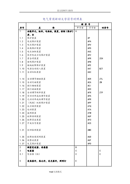
电气常用新旧文字符号对照表附表一二次回路接线图中常见的文字符号序号符号文字解释序号符号文字解释1 DL 继路器及其辅助触点 31 JSJ 加速继电器2 WJ 温度继电器 32 YZJ 电压中间继电器3 G 隔离开关及其辅助触点 33 ZXJ 指挥信号中间继电器4 WSJ 瓦丝继电器 34 WH 有功电度表5 LH 电流互感器 35 XKJ 选控继电器6 ZCH 重合闸继电器 36 VARH 无功电度表7 YH 电压互感器 37 XCJ 选测继电器8 BCJ 保护继电器 38 KK 控制开关9 HQ 合闸线圈 39 FJ 复归继电器10 ZJ 中间继电器 40 HK 转换开关11 HC 合闸接触器 41 ZZJ 重复中间继电器12 HWJ 合闸位置继电器 42 ZK 自动开关13 TQ 跳闸线圈 43 XZJ 信号中间继电器14 TWJ 跳闸位置继电器 44 CK 测量转换开关15 LJ 电流继电器 45 XJJ 信号监察继电器16 HJ 合闸继电器 46 XK 信号转换开关17 YJ 电压继电器 47 TBJ 跳跃闭锁继电器18 TJ 跳闸继电器 48 DK 刀开关19 SJ 时间继电器 49 YJJ 压力监视中间继电器20 TJJ 同步检测继电器 50 MK 灭磁开关21 CJ 差动继电器 51 A 电流表22 XMJ 信号脉冲继电器(冲击继电器) 52 LK 联动开关23 GJ 功率继电器 53 V 电压表24 JJ 监察继电器 54 XWK 限位开关25 XJ 信号继电器 55 W 有功功率表26 SXJ 事故信号中间继电器 56 XD 信号灯27 RJ 热继电器 57 WAR 无功功率表28 YXJ 预告信号中间继电器 58 LD 绿色信号灯29 BSJ 闭锁继电器 59 STK 手动同期转换开关30 HZ 频率表 60 QA 起动按钮续附表一序号符号文字解释序号符号文字解释61 HD 红色信号灯 91 YM 电压互感器二次电压小母线62 RD 熔断器 92 L 电感63 GD 光字牌 93 ZM 转角变压器小母线64 JRD 击穿保险 94 D 二极管65 WS 位置指示灯95 XDC 蓄电池66 RRD 弱电熔断器(热线轴) 96 BG 晶体三极管67 FM 蜂鸣器 97 Z 整流器68 KM 控制回路小母线 98 DS 电磁铁69 DO 电笛 99 R 电阻70 RKM 弱电控制回路电源小母线 100 LP 连接片71 JL 警铃 101 RF 附加电阻72 XM 信号回路电源小母线 102 QP 切换片73 HA 合闸按钮 103 BD 白色信号灯74 RXM 弱电信号回路电源小母线75 TA 跳闸按钮76 NQM 事故音响信号小母线77 FA 复归按钮78 +SM 闪光信号小母线79 ZXA 指挥信号按钮80 (+)HM 合闸电源小母线81 YJA 中央音响信号解除按钮82 FM 辅助小母线83 YA 试验按钮84 YBM 预告信号小母线85 SA 事故按钮86 RM 掉牌未复位“光字牌”87 THM 同期合同小母线88 ZYM 指挥装置音响小母线89 C 电容教学题目:二次接线图的识别教学目的:1、使学员认识到二次回路在发电厂和变电站中的重要性;2、学员能理解、掌握二次图中图形符号所对应的含义;3、让学员掌握绘制二次接线图的方法和原则;4、学员能阅读各种电气二次接线图。
灯管标准

F. COMPACT FL - LAMPS - 1.F-112~20MM TWIN TUBE LAMPS 两管灯A. SPK -系列用10MM 管径,是新型灯管,外型如 PL 灯。
也有U 形管。
B. SH -系列用12MM 管径,比照 PL 灯管制作。
也有U 形管。
FIG.1 C. SH -型配G23、GX23、2PIN 管座,进口起动器,适传统安定器。
D. SH4P -型配 2G7, 4PIN 管座,无起动器,为高频专用灯管,FIG.2适用汽车、游艇及紧急照明灯具。
E. LH -系列灯管,采用17MM 大管径,特殊管型设计,管壁承 受压力高,为高频专用灯管,使用于电子安定器时, 能充分发挥高频效率,延长灯管寿命。
F. XLH -系列灯管,管径 20MM ,提供GY10Q-4,4PIN 管座,为日本规格灯管。
G. 若使用电子安定器时,请选用高频专用灯管, 以配合高管壁压力。
FIG.5H. 高辉度灯管配合高演色性 RA=85 及平均寿命8,000小时以上。
I. 包装方式:有每支一纸盒之商品包装 及工業包裝,定貨時請指明。
SPK 10 MM H shaped 4pins lamps exteral start 无起跳器PL-灯管-7 7W G10q 58V 170 2500UW 20 130 112 FIG.3 200 -9 9W G10q 67V 170 3000UW 20 160 145 FIG.3 200 -11 11W G10q 75V 170 3500UW 20 180 160 FIG.3 200 -13 13W G10q 88V 170 4000UW 20 200 180 FIG.3 200 -15 15W G10q 96V 170 4500UW 20 230 210 FIG.3 200 SH T4 12MM single H,2 pins lamp with built in starter. 内装起跳器PL-灯管-5 5W G23 34V 190 250 28 108 70 FIG.1 200 -7 7W G23 47V 175 400 28 138 100 FIG.1 200 -9 9W G23 60V 170 600 28 168 130 FIG.1 200 -11 11W G23 91V 160 900 28 238 200 FIG.1 200 -13 13W GX23 58V 280 900 28 184 146 FIG.2 200 SH T4 12MM single H,4 pins lamp external starter for electronic ballast. 无起跳器PL-灯管-5 5W 2G7 27V 180 250 28 92 70 FIG.3 200 -7 7W 2G7 37V 175 400 28 122 100 FIG.3 200 -9 9W 2G7 48V 170 600 28 152 130 FIG.3 200 -11 11W 2G7 91V 160 900 28 222 200 FIG.3 200 -13 13W 2G7 60V 285 900 28 170 146 FIG.3 200 LH T6 17.5MM single H,high power 4 pins lamp. 欧规大功率无起跳器PL-灯管-18 18W 2G11 60V 370 1200 40 222 194 FIG.4 130 -26 26W 2G11 91V 340 1500 40 324 292 FIG.4 100 -36 36W 2G11 98V 430 2700 40 415 387 FIG.4 50 -40 40W 2G11 115V 360 3200 40 535 507 FIG.4 50 -55 55W 2G11 101V 670 4000 40 535 507 FIG.4 50 -80 80W 2G11 /145 /650 5100 40 568 540 FIG.4 25 -96 96W 2G11 /156 /850 6500 40 810 782 FIG.4 25XLH T7 20-22MM single H,big tube4 pins lamp 日规大管径无起跳器PL-灯管-18 18W GY10q-3 60V 375 1300 42 216 192 FIG.5 40 -27 27W GY10q-4 56V 610 1600 42 245 221 FIG.5 40 -36 36W GY10q-4 95V 435 2900 42 410 386 FIG.5 40 -40 40W GY10q-5 103V 435 3800 42 560 536 FIG.5 20 -55 55W GY10q-5 98V 670 4500 42 560 536 FIG.5 20 -96 96W GY10q-6 155V 820 7500 46 860 836 FIG.5 20W type VOLT MA LM D L1 L2 PCS/CTN DSH T4 12MM double H shaped 2 pins lamps with built in starter. 2H 内装起跳器美规灯管-13 13W GX23-2 60V 285 860 28 108 72 FIG.1 200DSU 220V 12MM double U shaped 2 pins lamps with built in starter. 2U内装起跳器欧规灯管-7 7W G23-2 47V 170 350 28 88 47 FIG.2 200-9 9W G23-2 58V 170 400 28 108 65 FIG.2 200 -10 10W G24d-1 64V 190 600 28 108 66 FIG.2 200-13 13W G24d-1 91V 170 900 28 119 75 FIG.2 100-18 18W G24d-2 100V 220 1200 28 153 109 FIG.3 100-22 22W G24d-3 103V 300 1600 28 161 117 FIG.4 100-26 26W G24d-3 107V 315 1800 28 172 128 FIG.4 100DSUE T4 12MM double U shaped 4 pins lamp with external starter. 2U欧规无起跳器灯管-10 10W G24q-1 64V 190 600 28 97 66 FIG.2 100-13 13W G24q-1 91V 165 900 28 109 75 FIG.2 100-18 18W G24q-2 100V 220 1200 28 142 109 FIG.3 100-22 22W G24q-3 103V 300 1600 28 150 117 FIG.4 100 -26 26W G24q-3 107V 315 1800 28 161 128 FIG.4 100DMH T5 15MM double H(PLC),2 pins lamps with built in starter. 美规无起跳器PLC-灯管-18 18W GX23-2 57V 285 860 38 119 78 FIG.5 200-22 22W GX32d-2 60V 450 1200 38 151 110 FIG.5 100-28 28W GX32d-3 60V 600 1600 38 163 122 FIG.5 100 DLHE T6 17MM double H shaped 4 pins lamps with external starter. 日规无起跳器BB 灯管-13 13W GX10q-2 54V 375 900 40 114 74 FIG.6 100 -18 18W GX10q-3 60V 450 1070 40 127 97 FIG.6 100 -27 27W GX10q-4 60V 610 1600 40 141 111 FIG.6 100F. COMPACT FL - LAMPS - 3.F-3A.B. 3支U是常称之3UC. 3U型灯管提供12MM及15MM两种管径供选择。
Freescale 双极性LDMOS宽带集成功率放大器数据表说明书

MW7IC008NT1MW7IC008NT11RF LDMOS Wideband Integrated Power AmplifierThe MW7IC008N wideband integrated circuit is designed with on--chip matching that makes it usable from 20to 1000MHz.This multi--stage structure is rated for 24to 32volt operation and covers most narrow bandwidth communication application formats.Driver Applications∙Typical CW Performance:V DD =28Volts,I DQ1=25mA,I DQ2=75mAFrequency G ps (dB)PAE (%)100MHz @11W CW 23.555400MHz @9W CW 22.541900MHz @6.5W CW23.534∙Capable of Handling 10:1VSWR,@32Vdc,900MHz,P out =6.5Watts CW (3dB Input Overdrive from Rated P out )∙Stable into a 5:1VSWR.All Spurs Below --60dBc @1mW to 8Watts CW P out @900MHz∙Typical P out @1dB Compression Point ≃11Watts CW @100MHz,9Watts CW @400MHz,6.5Watts CW @900MHz Features∙Broadband,Single Matching Network from 20to 1000MHz∙Integrated Quiescent Current Temperature Compensation with Enable/Disable Function (1)∙Integrated ESD Protection∙In Tape and Reel.T1Suffix =1,000Units,16mm Tape Width,13--inch Reel.Figure 2.Pin Connections123456789101112181716151413242322212019NC V T T S 1V G L S 2N CR F i n S 2R F o u t S 1/V D S 1N C N CN C N CRF outS2/V DS2NC V G S 2V T T S 2NC NC NC NCN C V GS1RF inS1NC NC V GLS11.Refer to AN1977,Quiescent Current Thermal Tracking Circuit in the RF Integrated Circuit Family and to AN1987,Quiescent Current Control for the RF Integrated Circuit Device Family .Go to /rf.Select Documentation/Application Notes --AN1977or AN1987.Document Number:MW7IC008NRev.3,12/2013Freescale Semiconductor Technical Data100--1000MHz,8W PEAK,28V RF LDMOS WIDEBANDINTEGRATED POWER AMPLIFIERMW7IC008NT12RF Device DataFreescale Semiconductor,Inc.MW7IC008NT1Table 1.Maximum RatingsRatingSymbol Value Unit Drain--Source Voltage V DSS --0.5,+65Vdc Gate--Source Voltage V GS --6.0,+12Vdc Operating VoltageV DD 32,+0Vdc Storage Temperature Range T stg --65to +150︒C Operating Junction Temperature T J 150︒C 100MHz CW Operation @T A =25︒C (3)400MHz CW Operation @T A =25︒C (3)900MHz CW Operation @T A =25︒C (3)CW1165W W W Input Power100MHz 400MHz 900MHzP in 272338dBmTable 2.Thermal CharacteristicsCharacteristicSymbol Value (1,2)Unit Thermal Resistance,Junction to Case (CW Signal @100MHz)(Case Temperature 82︒C,P out =11W CW)Stage 1,28Vdc,I DQ1=25mA Stage 2,28Vdc,I DQ2=75mA (CW Signal @400MHz)(Case Temperature 87︒C,P out =9W CW)Stage 1,28Vdc,I DQ1=25mA Stage 2,28Vdc,I DQ2=75mA (CW Signal @900MHz)(Case Temperature 86︒C,P out =6.5W CW)Stage 1,28Vdc,I DQ1=25mA Stage 2,28Vdc,I DQ2=75mAR θJC5.34.94.42.73.53.2︒C/WTable 3.ESD Protection CharacteristicsTest MethodologyClass Human Body Model (per JESD22--A114)1B Machine Model (per EIA/JESD22--A115)A Charge Device Model (per JESD22--C101)IIITable 4.Moisture Sensitivity LevelTest MethodologyRating Package Peak TemperatureUnit Per JESD22--A113,IPC/JEDEC J--STD--0203260︒C1.MTTF calculator available at /rf.Select Software &Tools/Development Tools/Calculators to access MTTF calculators by product.2.Refer to AN1955,Thermal Measurement Methodology of RF Power Amplifiers.Go to /rf.Select Documentation/Application Notes --AN1955.3.CW Ratings at the individual frequencies are limited by a 100--year MTTF requirement.See MTTF calculator (referenced in Note 1).MW7IC008NT13RF Device DataFreescale Semiconductor,Inc.Table 5.Electrical Characteristics (T A =25︒C unless otherwise noted)CharacteristicSymbolMinTypMaxUnitStage 1—Off CharacteristicsZero Gate Voltage Drain Leakage Current (V DS =65Vdc,V GS =0Vdc)I DSS ——10μAdc Zero Gate Voltage Drain Leakage Current (V DS =28Vdc,V GS =0Vdc)I DSS ——1μAdc Gate--Source Leakage Current (V GS =1.5Vdc,V DS =0Vdc)I GSS——10μAdcStage 1—On Characteristics Gate Threshold Voltage(V DS =10Vdc,I D =5.3μAdc)V GS(th) 1.32 2.8Vdc Gate Quiescent Voltage(V DD =28Vdc,I D =25mAdc,Measured in Functional Test)V GS(Q)22.83.5VdcStage 2—Off CharacteristicsZero Gate Voltage Drain Leakage Current (V DS =65Vdc,V GS =0Vdc)I DSS ——10μAdc Zero Gate Voltage Drain Leakage Current (V DS =28Vdc,V GS =0Vdc)I DSS ——1μAdc Gate--Source Leakage Current (V GS =1.5Vdc,V DS =0Vdc)I GSS——10μAdcStage 2—On Characteristics Gate Threshold Voltage(V DS =10Vdc,I D =23μAdc)V GS(th) 1.32 2.8Vdc Gate Quiescent Voltage(V DD =28Vdc,I D =75mAdc,Measured in Functional Test)V GS(Q)2 2.7 3.5Vdc Drain--Source On--Voltage(V GS =10Vdc,I D =3.6Adc)V DS(on)0.10.31VdcFunctional Tests (1)(In Freescale Test Fixture,50ohm system)V DD =28Vdc,I DQ1=25mA,I DQ2=75mA,P out =6.5W CW,f =900MHzPower GainG ps 21.523.531.5dB Power Added Efficiency PAE 3034—%Input Return LossIRL—--15--11dB Typical Broadband Performance (In Freescale Test Fixture,50ohm system)V DD =28Vdc,I DQ1=25mA,I DQ2=75mAFrequency G ps (dB)PAE (%)IRL (dB)100MHz @11W CW 23.555--20400MHz @9W CW 22.541--17900MHz @6.5W CW23.534--151.Part internally matched both on input and output.(continued)4RF Device DataFreescale Semiconductor,Inc.MW7IC008NT1Table 5.Electrical Characteristics (T A =25︒C unless otherwise noted)(continued)Characteristic Symbol Min Typ Max Unit Typical Performances (In Freescale Test Fixture,50ohm system)V DD =28Vdc,I DQ1=25mA,I DQ2=75mA,100--1000MHz BandwidthCharacteristicSymbol Min Typ Max Unit IMD Symmetry @6.8W PEP ,P out where IMD Third Order Intermodulation 30dBc (1)(Delta IMD Third Order Intermodulation between Upper and Lower Sidebands >2dB)IMD sym—0.1—MHzVBW Resonance Point (1)(IMD Third Order Intermodulation Inflection Point)VBW res —0.1—MHz Gain Flatness in 500--1000MHz Bandwidth @P out =6W Avg.G F — 1.35—dB Gain Variation over Temperature (--30︒C to +85︒C)∆G —0.024—dB/︒C Output Power Variation over Temperature (--30︒C to +85︒C)∆P1dB—0.005—dB/︒CTypical CW Performances —100MHz (In Freescale Test Fixture,50ohm system)V DD =28Vdc,I DQ1=25mA,I DQ2=75mA,P out =11W CW,f =100MHz Power GainG ps —23.5—dB Power Added Efficiency PAE —55—%Input Return LossIRL —--20—dB P out @1dB Compression Point,CWP1dB—11—WTypical CW Performances —400MHz (In Freescale Test Fixture,50ohm system)V DD =28Vdc,I DQ1=25mA,I DQ2=75mA,P out =9W CW,f =400MHz Power GainG ps—22.5—dB Power Added Efficiency PAE —41—%Input Return LossIRL —--17—dB P out @1dB Compression Point,CWP1dB—9—WTypical CW Performances —900MHz (In Freescale Test Fixture,50ohm system)V DD =28Vdc,I DQ1=25mA,I DQ2=75mA,P out =6.5W CW,f =900MHz Power GainG ps —23.5—dB Power Added Efficiency PAE —34—%Input Return LossIRL —--15—dB P out @1dB Compression Point,CWP1dB—6.5—W1.Not recommended for wide instantaneous bandwidth modulated signals.MW7IC008NT15RF Device DataFreescale Semiconductor,Inc.Figure 3.MW7IC008NT1Test Circuit Component LayoutTable 6.MW7IC008NT1Test Circuit Component Designations and ValuesPartDescriptionPart NumberManufacturer C10.01μF Chip Capacitor GRM3195C1E103JA01Murata C2,C150.1μF Chip Capacitors GRM219F51H104ZA01Murata C3,C1610μF Chip Capacitors GRM55DR61H106KA88L Murata C4,C5,C7,C8,C10,C11,C12,C140.01μF Chip Capacitors C0805C103K5RAC Kemet C6,C171μF,35V Tantalum Capacitors TAJA105K035R AVX C9 2.2pF Chip Capacitor ATC600S2R2CT250XT ATC C13 3.3pF Chip CapacitorATC600S3R3BT250XT ATC L1,L7150nH Ceramic Chip Inductors LL2012--FHLR15J Toko L2,L6180nH Ceramic Chip Inductors LL2012--FHLR18J Toko L3 1.6nH Inductor 0603HC--1N6XJLW Coilcraft L4,L5 5.1nH Inductors0603HP--5N1XJLW Coilcraft R1,R12510Ω,1/10W Chip Resistors RR1220P--511--B--T5Susumu R2,R3,R491Ω,1/8W Chip Resistors CRCW080591R0FKEA Vishay R5*,R9*0Ω,2.5A Chip Resistors CRCW08050000Z0EA Vishay R610K Ω,1/8W Chip Resistor CRCW080510K0JNEA Vishay R7,R1112K Ω,1/8W Chip Resistors CRCW080512K0JNEA Vishay R843Ω,1/8W Chip Resistor CRCW080543R0FKEA Vishay R1015K Ω,1/8W Chip Resistor CRCW080515K0JNEA Vishay PCB0.020",εr =3.66RO4350BRogers*Add for temperature compensation6RF Device DataFreescale Semiconductor,Inc.MW7IC008NT1TYPICAL CHARACTERISTICSG p s ,P O W E R G A I N (d B )1000100f,FREQUENCY (MHz)Figure 4.Broadband Performance @P in =14.6dBm CW600400300--307060504030--5--10--15I R L ,I N P U T R E T U R N L O S S (d B )4121086P A E ,P O W E R A D D E D E F F I C I EN C Y (%)500200800700--20--2514P o u t ,O U T P U T P O W E R (W A T T S )900Figure 5.Intermodulation Distortion Productsversus Two--Tone SpacingTWO--TONE SPACING (MHz)10--20--401200I M D ,I N T E R M O D U L A T I O N D I S T O R T I O N (d Bc )--60--30--50--10P out ,OUTPUT POWER (WATTS)CWFigure 6.Power Gain and Power AddedEfficiency versus Output Power18109080706050P A E ,P O W E R A D D E D E F F I C I E N C Y (%)G p s ,P O W E R G A I N (d B )2625402423222120193020100MW7IC008NT17RF Device DataFreescale Semiconductor,Inc.TYPICAL CHARACTERISTICSFigure 7.Broadband Frequency Responsef,FREQUENCY (MHz)200G A I N (d B )4006008001000120014001600-36I R L (d B )8RF Device DataFreescale Semiconductor,Inc.MW7IC008NT1V DD =28Vdc,I DQ1=25mA,I DQ2=75mAP out =11W @100MHz,9W @400MHz,6.5W @900MHz f MHz Z in ΩZ load Ω10049.78+j1.0747.87--j9.8515048.96+j1.4449.12--j5.4420048.00+j1.5449.09--j2.6625046.67+j1.3648.63--j0.7930045.30+j0.9147.73+j0.4935043.93+j0.1146.60+j1.2240042.53--j0.8645.63+j1.4345041.38--j2.1644.97+j1.1350040.30--j3.7145.04+j0.7055039.38--j5.4445.23+j0.7760038.43--j7.1144.80+j1.2965037.94--j8.7144.32+j1.4870037.49--j10.5243.57+j1.5175037.31--j12.4243.19+j1.3280037.00--j14.0342.61+j0.7785036.74--j15.6442.25+j0.3990036.57--j17.0941.90+j0.0395036.37--j18.5941.67--j0.41100036.12--j20.0641.77--j1.10105035.58--j21.4341.82--j1.60110035.00--j22.7941.90--j2.01115034.53--j24.3942.26--j2.43120033.53--j25.9742.51--j2.80125032.67--j27.8442.74--j2.99130031.61--j29.8943.10--j3.11135030.61--j32.3443.52--j3.19140029.55--j34.8143.86--j3.13145028.23--j37.6144.03--j3.03150027.34--j40.5944.33--j2.67Z in=Device input impedance as measured from gate to ground.Z load =Test circuit impedance as measured from drain to ground.Figure 8.Series Equivalent Input and Load ImpedanceZinZloadOutput Matching NetworkMW7IC008NT19RF Device DataFreescale Semiconductor,Inc.PACKAGEDIMENSIONS10RF Device Data Freescale Semiconductor,Inc.MW7IC008NT1MW7IC008NT111RF Device Data Freescale Semiconductor,Inc.12RF Device Data Freescale Semiconductor,Inc.MW7IC008NT1PRODUCT DOCUMENTATION AND SOFTWARERefer to the following documents and software to aid your design process.Application Notes∙AN1955:Thermal Measurement Methodology of RF Power Amplifiers∙AN1977Quiescent Current Thermal Tracking Circuit in the RF Integrated Circuit Family∙AN1987Quiescent Current Control for the RF Integrated Circuit Device FamilyEngineering Bulletins∙EB212:Using Data Sheet Impedances for RF LDMOS DevicesSoftware∙Electromigration MTTF Calculator∙RF High Power Model∙.s2p FileFor Software,do a Part Number search at ,and select the “Part Number”link.Go to the Software &Tools tab on the part’s Product Summary page to download the respective tool.REVISION HISTORYThe following table summarizes revisions to this document.RevisionDate Description 0Aug.2009∙Initial Release of Data Sheet 1Sept.2009∙Modified Fig.3,Test Circuit Component Layout and Table 6,Test Circuit Component Designations andValues to include temperature compensation options,p.5∙Fig.3,Test Circuit Component Layout,corrected V DD1to V GG1,p.5∙Table 6,Test Circuit Component Designations and Values,C6,C17:updated description from “1μF Tantalum Capacitors”to “1μF,35V Tantalum Capacitors”;L1,L7,L2,L6:corrected manufacturer fromCoilcraft to Toko;L3:corrected part number from “0603HC--1N6XJLC”to “0603HC--1N6XJLW”;L4,L5:corrected part number from “100B100JT500XT”to “0603HP--5N1XJLW”;R1,R12:updated descriptionfrom “510ΩChip Resistors”to “510Ω,1/10W Chip Resistors”,p.52Mar.2011∙Updated frequency in overview paragraph from “100to 1000MHz”to “20to 1000MHz”to reflect lower20MHz capability and narrow bandwidth modulation,p.1∙Updated IMD sym Typical value from 180MHz to 0.1MHz and VBW res Typical value from 210MHz to0.1MHz;modified Footnote 1to reflect limited device capability regarding wide video bandwidth,TypicalPerformance table,p.42.1Mar.2012∙Table 3,ESD Protection Characteristics,removed the word “Minimum”after the ESD class rating.ESDratings are characterized during new product development but are not 100%tested during production.ESDratings provided in the data sheet are intended to be used as a guideline when handling ESD sensitivedevices,p.23Dec.2013∙Table 6,Test Circuit Component Designations and Values:updated PCB description to reflect mostcurrent board specifications from Rogers,p.5∙Replaced Case Outline 98ASA10760D,Rev.O with Rev.A,pp.9--11.Mechanical outline drawing modified to reflect the correct lead end features.Format of the mechanical outline was also updated to thecurrent Freescale format for Freescale mechanical outlines.MW7IC008NT113Informationin this document is provided solely to enable system and software implementers to use Freescale products.There are no express or implied copyright licenses granted hereunder to design or fabricate any integrated circuits based on the information in this document.Freescale reserves the right to make changes without further notice to any products herein.Freescale makes no warranty,representation,or guarantee regarding the suitability of its products for any particular purpose,nor does Freescale assume any liability arising out of the application or use of any product or circuit,and specifically disclaims any and all liability,including without limitation consequential or incidental damages.“Typical”parameters that may be provided in Freescale data sheets and/or specifications can and do vary in different applications,and actual performance may vary over time.All operating parameters,including “typicals,”must be validated for each customer application by customer’s technical experts.Freescale does not convey any license under its patent rights nor the rights of others.Freescale sells products pursuant to standard terms and conditions of sale,which can be found at the following address:/SalesTermsandConditions.Freescale and the Freescale logo are trademarks of Freescale Semiconductor,Inc.,Reg.U.S.Pat.&Tm.Off.All other product or service names are the property of their respective owners.E 2009,2011--2013Freescale Semiconductor,Inc.How to Reach Us:Home Page: Web Support:/supportMW7IC008NT1。
Philips Respironics DreamStation PAP系统用户指南说明书

Key Content A veteran’s guide to DreamStation PAP systemsPAP systems brochureVeterans a airsDream StationProudly designed and engineered in the USANatural. Comfortable. Sleep.Philips Respironics DreamStation supports long-term patient use while helping to creating new efficiencies for your facility Proud to serve veterans*In a retrospective review conducted by Philips Respironics of approximately 15,000 System One patients, patients who used SleepMapper, which has been rebranded to DreamMapper,demonstrated 22% greater adherence to the therapy than patients who did not use SleepMapper. To see a list of compatible DreamMapper devices, go to /compatible.Powerful patient-driven designDreamStation was designed with feedback from hundreds ofpatients to provide a simple CPAP experience to help bothnew and experienced patients use therapy long-term. A suiteof intuitive tools can be customized by healthcare professionalsto choose the solution that’s right for each patient.Acclimating patients in the early days of therapyEZ-Start can help patients gradually adapt to their prescribedlevel of therapy using an innovative pressure acclimationalgorithm with automatic, personalized adjustments to CPAPpressure during the first 30 days.SmartRamp helps users to fall asleep to lower pressures thanthose of standard ramp mode. The air pressure remains low untilthe patient experiences an obstructive respiratory event. ThenSmartRamp responds with an auto algorithm to resolvethe patient’s apneas.Make progress every dayEach morning, patients are greeted with Daily ProgressFeedback — a summary of how far they’ve come — to motivatethem to stick with their therapy. The intuitive, color displayshows a simple trend of their nightly hours of use, followedby a summary of their last 30 days of good nights — those withmore than four hours of use.Sleep therapy success* at your patients’ fingertips Bluetooth® is included in every DreamStation device for easy connectivity to the DreamMapper patient self-management tool. DreamMapper helps patients take an active role in their sleep management by providing daily therapy progress, helpful troubleshooting videos and goal-setting tools. Patients can stay engaged and get the information they need fast, without having to use your staff’s time to resolve common issues.An Encore performance DreamStation connects to our powerful Encore Anywhere patient compliance management software. Encore Anywhere makes it easy and efficient for sleep professionals to manage patient compliance and therapy.Focus your time where it belongs Encore Anywhere features Adherence Profiler and Care Orchestrator. It’s an optional, intuitive tool that helps you identify patients according to their probability of achieving adherence, helping focus your staff’s time on the patients who have the greatest likelihood of success.Simplify device evaluation Performance Check simplifies in-home device evaluation for easy remote troubleshooting. Designed to reduce the time and frustration involved in device troubleshooting, this robust tool allows you to guide the patient through an easy remote diagnosis, resulting in a simple “Pass/Fail” result to determine if the device needs to be returned for service.Performance Check can also generate a report in ourEncore Anywhere patient management software tool,allowing you to troubleshoot patient concerns.According to our research, 25% of returned devices are found to be operating normally.* Performance Check is designed to help reduce the number of normally functioning devices thatare returned for service, saving you time and delivery costs.Reduce manual adjustments DreamStation can automatically adjust to changing patient needs, helping improve workflow processes and letting you focus your attention where it needs to be.CPAP-CheckChecks on the user every 30 hours to determine if CPAPpressure is optimal. If not, it automatically adjusts to meetchanging patient needs.Auto-TrialDelivers breath-by-breath auto-CPAP therapy for up to atotal of 30 days per patient. Transitions to CPAP or CPAP-Check mode at end of Auto-Trial.Opti-StartProvides optimal starting pressure that can enhance patientcomfort and reduce the likelihood of residual events at thebeginning of therapy.Creating efficiencies that make a difference*Philips research, 2015Only DreamStation offers Wi-Fi, Bluetooth ®and cellular connectivity options. By providingthe most comprehensive suite of connectivitychoices among leading CPAP brands *, you canchoose the options that are best for your sleepprogram. DreamStation’s innovative designhas the capability to adapt as technologiescontinue to advance.Making it easy to reach your patients• Wi-Fi delivers daily data to clinicians and provides coverage even inweak cellular areas• Bluetooth is included in every device for easy connectivity withDreamMapper and Alice NightOne• Cellular provides data on a daily basis and one hour after the patienthas turned the device off More connectivity options to provide easy access to patient data*Internal assessment of 2015 competitive CPAP data comparing to ResMed Airsense10/Aircurve10 platform and Fisher & Paykel Iconseries platform.The Philips Respironics DreamMapper helps patientstake an active role in their therapyInspire patients Tools to help encourage adherenceTroubleshootTroubleshoot commonproblems With the DreamMapper self-management tool, patients can use the mobileand web-based features to engage with their therapy.30% smaller 39%lighter63%quieter“Good-looking piece of equipment! It’s modern looking, doesn’t look like a medical machine. It’s quieter, too.”“I liked it as soon as I opened it! I liked the way it was laid out and I liked the size of it — it was small, easy to fit on a table along with a lamp and my phone.”DreamStation usersFive-year DreamStation VA warrantyPhilips Respironics is proud to offera five-year warranty on all of ourDreamStation sleep therapy productswhen purchased through First NationGroup, FSS, ECAT, MSPV and otherauthorized procurement channels.Philips Respironics commitment to qualityInsight-driven i nnovationIntuitive menu system Graphics-based menu inspired by smartphone navigation for ease of use Ambient light sensor Automatically adjusts screen brightnessfor daytime or nighttime viewingIntegrated Bluetooth®Wirelessly connectswith DreamMapper orAlice NightOne portablesleep diagnostic systemDaily progress feedbackDisplays previous threenights’ therapy resultsto track progressTop-mounted hose outletSwivel outlet rotates 180˚for freedom of movementDetachable humidifierThe humidifier separatesto travel even lighterSimplified designEasy access to waterchamber for fillingand cleaningTwo-step airfiltration systemUltra-fine filterprovides additionalfiltration of veryfine particlesSD card andcompliance codesEasily share sleep datawith the care teamProudly designed andengineered in the USAPart number DSX500S11DSX500H11C DSX500T11C Part number DSXH 11225201120613Part number 111849910058941124009112173611277991126947Part number PR15HT15Part number 1122446112244711225181122519Part number 11202931121694Part number 100603C 100604C 100700W 100705W Part number 11147841121162112074711201351124301Part number11221351124224Part number DSX700S11DSX700H11C DSX700T11C Part number DSX1030S11DSX1030H11C DSX1030T11C Part number DSX1130S11DSX1130H11C DSX1130T11C DreamStation Auto CPAPDreamStation Auto CPAPDreamStation Auto CPAP with humidifierand cellular modemDreamStation Auto CPAP with humidifier,heated tube and cellular modem Humidification DreamStation humidifier DreamStation water chamber DreamStation humidifier dry box inlet seal Power managementDreamStation 80-watt power supply6 ft power cordPAP Lithium Ion battery kit**Li Ion battery, PAP device cable Li Ion battery, cable adapter (50 series adapter, 2/each)Li Ion battery case Tubes15mm 6 ft standard tube15mm 6 ft heated tubeFilters Pollen filter, reusable (1 per pack)Ultra-fine filter, disposable (1 per pack) Ultra-fine filter, disposable (2 per pack)Ultra-fine filter, disposable (6 per pack)Accessories Link module Nonin SpO 2, assembly Modems Cellular modem, oximetry capable Cellular modem, non-oximetry Wi-Fi accessory, oximetry capable Wi-Fi accessory, non-oximetry Travel accessories Universal PAP/laptop travel briefcase DreamStation replacement carrying case Shielded 12V DC power cord system(includes shielded DC cord andbattery adapter cable)DreamStation travel case, 65W powersupply* w/ USB portDreamStation travel case, 65W powersupply* w/ USB port, 5/caseMask and tubing bedside organizer Bedside organizer Bedside organizer, 10/case DreamStation Auto BiPAPDreamStation Auto BiPAPDreamStation Auto BiPAP with humidifierand cellular modemDreamStation Auto BiPAP with humidifier,heated tube and cellular modem DreamStation BiPAP S/TDreamStation BiPAP S/TDreamStation BiPAP S/T with humidifierand cellular modemDreamStation BiPAP S/T with humidifier,heated tube and cellular modemDreamStation BiPAP AVAPSDreamStation BiPAP AVAPSDreamStation BiPAP AVAPS with humidifierand cellular modemDreamStation BiPAP AVAPS with humidifier,heated tube and cellular modem Ordering informationDreamStation BiPAP autoSVDreamStation BiPAP autoSV with humidifierand cellular modemDreamStation BiPAP autoSV with humidifier,heated tube and cellular modem Part number DSX900H11C DSX900T11CPhilips Respironics is proud to have its worldwide headquarters in the USA Going further for youThe Philips Respironics RIST facility, located 20 miles eastof Pittsburgh, PA, is home to our sleep and home respiratory division. This 172,000-square-foot greenfield facility was awarded LEED Gold certification in 2009 and was chosenby Assembly Magazine as the Assembly Plant of the Year.*Our USA-based team takes pride in their work because they know there’s always a way to make life better for all of our customers – including veterans like you.Proudly designed andengineered in the USATo order product, contact First Nation: Fax: 734 929 1490Phone: 800 541 2071Email:***************************To contact Philips Respironics, call 800 345 6443 andfollow the prompt as noted below:• Customer service: press 1• Repair/return/warranty questions: press 2, then press 7• Product support: press 4724 387 4000。
MR-E 三菱伺服样本

15.9
24
62
152
93
—
310
—
—
456
930
—
—
760
11.9
17.8
14.0
20.0
伺服电机转动惯量的15倍以下(注4)
增量型编码器(伺服电机每转的分辨率:131,072p/rev)
—
全封闭自冷式(保护方式IP67)(注5)
0~40℃(无冰冻) 保存温度:-15~70℃(无冰冻)
80%RH以下(无结露) 保存湿度:90%RH(无结露)
带电磁制动器
6.7
7.6
10
17
注: 1. 电源设备的功率因电源阻抗而变。
2. 再生制动器频度表示在空载和无再生制动选件情况下单体电机由额定转速起减速停止时的允许频度。但是,在带有负载时是表中数值的1/(m+1)(m=负载转动惯量/电机转动惯量)。另外,
如果超过额定转速,则再生制动器频度与(运转速度/额定速度)的平方成反比。如果转速频繁变动,例如,上下进给动作时处于长时间再生状态那样的情况下,要求出运转时的再生发热量(W),
伺服电机HF-KN□-S100系列的转矩特性
HF-KN13(B)J-S100(注1,2)
140
1.0
短时间运转区域
105
0.75
HF-KN23(B)J-S100(注1,2)
280
2.0
短时间运转区域
210
1.5
HF-KN43(B)J-S100(注1,2)
560
4.0
短时间运转区域
420
3.0
转矩 (oz·in) 转矩(N·m)
4. 实际转矩如果在额定范围内,则再生频度无限制值。但是,推荐负载转动惯量比为15倍以下。 5. 负载转动惯量比如果超过表中的值,请向我公司咨询。
科尔摩根AKM 同步伺服电机 选型指南说明书
K O L L M O R G E N | A K o l l m o r g e n C O M PA N Y欢迎来到科尔摩根官方微信科尔摩根3目录u AKM ™ 同步伺服电机4u AKD ™ 伺服驱动器8u AKM ™ 各种选件12u AKM ™ 防水型和食品级防水型电机13u AKM ™ 系统综述14u AKM ™ 图纸和性能数据AKM1x 16AKM2x 20AKM3x24AKM4x 28AKM5x 34AKM6x 40AKM7x 44AKM8x48u L 10 轴承疲劳寿命和轴负载53u 反馈选件56u 抱闸选件60u 伺服电机连接器选件61u 型号命名67u MOTIONEERING ® Online71科尔摩根A K M 同步伺服电机选型指南克服设计、采购和时间障碍科尔摩根明白:帮助原始设备制造商的工程师克服障碍,可以显著提高其工作成效。
因而,我们主要通过如下三种方式来提供帮助:集成标准和定制产品在很多情况下,理想方案都不是一成不变的。
我们拥有专业应用知识,可以根据全面的产品组合来修改标准产品或开发全定制解决方案,从而为设计奠定良好的基础。
提供运动控制解决方案而不仅仅是部件在各公司减少供应商数量和工程人力的过程中,他们需要一家能够提供多种集成解决方案的全系统供应商。
科尔摩根就采用了全面响应模式,为客户提供全套解决方案,这些方案将编程软件、工程服务以及同类优秀的运动控制部件结合起来。
覆盖全球我们在美洲、欧洲、中东和亚洲拥有众多直销、工程支持单位、生产工厂以及分销商,临近全球各地的原始设备制造商。
这种便利优势可以加速我们的供货过程,根据客户需要随时随地供货。
财务和运营稳定性科尔摩根隶属于Fortive 公司。
Fortive 业务系统是推动Fortive 各部门发展的一个关键力量。
该系统采用“不断改善”(Kaizen )原理。
由高素质人才构成的多学科团队使用世界级的工具对过程进行评估,并制定相关计划以达到卓越的性能。
星辰伺服驱动说明书
NAS 系列交流伺服系统使用说明书特别提示在您第一次接通本伺服系统电源以前,为确保系统能安全、正常、高效地为您工作,请仔细阅读手册中有关使用方面的重要信息。
感谢使用星辰伺服的交流伺服系统!为使本机一直维持良好的运行状态,请将本手册随整机附送给最终用户。
虽然在您的选型过程中,可能已经对本产品有所了解并与本公司的技术人员进行了某些沟通,但为充分发挥本机最佳功能,仍请在使用前,仔细阅读本使用说明书,必要时可与星辰伺服的有关人员联系以获得必要的帮助。
本说明书中,对不同级别的提示、警示、警告采用如下提示符:★一般性的提示警示,如果不按照执行,可能带来设备的损坏警告,如果不按照执行可能带来设备严重损坏、火灾或人身伤害星辰伺服分支机构及技术服务机构:桂林星辰电力电子有限公司市场服务部地址:桂林高新技术产业开发区星辰大厦邮编:541004电话:************,5810692 传真:************ Email:******************上海星之辰电气传动技术有限公司伺服部地址:上海市科技创业中心(徐汇区钦州路100号)2#601-605 邮编:200235电话:************(8线), 64829055 传真:************深圳市星辰激光技术有限公司伺服部地址:深圳市高新区北区清华信息港研发楼A栋3楼邮编:518057电话:*************(15线),26030572 传真:*************目录1.安全注意事项1.1.安装注意事项1.2.运转操作注意事项1.3.保养检查注意事项1.4.关于废弃1.5.其它2.产品的确认和注意事项2.1.产品的确认2.2.伺服电机型号说明2.3.伺服驱动器型号说明2.4.使用前的注意事项3.NAS系列交流伺服系统性能参数3.1.NAS系列伺服系统标准规格配套表3.2.驱动器标准规格及功能表3.2.1.驱动器标准规格及一般功能3.2.2.驱动器使用环境条件及一般技术状态3.2.3.驱动器控制功能及运动性能表3.2.4.伺服电机特性3.2.4.1.N系列电机3.2.4.2.SY系列电机3.2.5.有关工作制的说明4.安装4.1.安装场所和保养4.2.驱动器外形尺寸4.3.驱动器安装4.4.驱动器前级盒的拆卸和安装4.5.伺服电机外形尺寸4.6.伺服电机安装4.7.制动电阻安装5.端口说明及外围电路设计5.1.接线注意事项5.2.外围接线图及端口说明5.2.1.控制接口(44芯排插头)全部功能连接图5.2.2.控制接口(44芯排插头)接口功能表5.2.3.状态通报口的使用5.2.4.模拟量接口的使用5.2.5.转矩环控制运行5.2.6.速度环控制运行5.2.7.带速度限制的位置环控制运行5.2.8.带转矩限制的位置环控制运行5.2.9.带转矩限制的速度环控制运行5.2.10.带转矩偏置的速度环控制运行5.2.11.位置环脉冲给定接口的使用5.2.12.反馈接口(15芯排插头)的连接5.2.13.反馈接口(15芯排插头)端口功能表5.2.14. RS485接口(9芯排插头)的连接5.2.15. RS485接口(9芯排插头)端口功能表5.2.16.动力接口6.操作面板6.1.面板显示说明6.1.1.监视状态下驱动器面板显示状态表6.1.2.运行状态下驱动器面板显示状态表6.2.面板操作说明及编辑状态下面板显示6.2.1.几种典型的操作6.2.2.编辑状态下的显示7.运转7.1.运转前的检查7.2.首次上电和试运转7.3.运转7.3.1.功能、参数设定总表7.3.2.位置闭环运行7.3.3.速度闭环运行7.3.4.转矩环运行8.RS485串行通讯功能8.1.概述8.2.通过RS485串行通讯进行伺服驱动器的运转8.2.1.状态查询8.2.2.修改参数8.2.3.实时控制8.3.TB485-V10通讯协议8.3.1.串口通讯数据格式8.3.2.工作方式说明8.3.2.1.问答方式8.3.2.2.速传方式8.3.3.通讯故障约定及校验说明8.3.3.1.问答方式8.3.3.2.速传方式9.保护功能9.1.设定方法(功能代码显示模式)9.2.功能代码一览表9.3.功能说明10.故障确认11.保养和检查11.1.保养和检查时的注意事项11.2.检查项目11.3.兆欧表测试11.4.零部件的更换安全注意事项1.安全注意事项1.1.安装注意事项★ 安装环境:使用温度伺服电机 -20℃~+40℃伺服驱动器 -10℃~+40℃保存温度-25℃~+65℃环境湿热伺服电机 95%,30℃,不结露伺服驱动器 90%,30℃,不结露标准高度海拔2000m以下(2000m以上,每上升1000m降容20%)★ 请将电机和驱动器安装于通风良好的场所。
信号工考试:地铁信号工考点巩固(强化练习)
信号工考试:地铁信号工考点巩固(强化练习)1、问答题简述FTGS接收器1板的功能。
正确答案:接收器1板用来”•算轨道信号电压幅度,在这块板上,根据运行方向、区段长度和绝缘方式,设置响应值。
轨道空闲时,接收器1板向解调器板发送脉冲(江南博哥),向接收器2板提供DC电压。
2、多选常见的混线故障有OβA、自混B、互混C、单线接地。
正确答案:A,B,C3、单选每台分辨器可控制O台PDP/1.CD显示屏。
A.7B.8C.9D.10正确答案:B4、单选近地强信号干扰远地弱信号的现象称为O0A、远近效应B、呼吸效应C、多径效应D、阴影效应正确答案:A5、多选程控交换机的运行软件大致可分为OoA.数据B.系统程序C.应用程序D.专用程序正确答案:B,C6、填空题在已成功登陆1.OW后,可以通过点击()按钮来退出1.(W操作系统,系统回复到登记进入状态。
正确答案:注销7、判断题广播系统中运营控制中心和各车站均能独立操作。
正确答案:对8、判断题水平(垂直)波瓣宽度是定向天线常用的一个很重要的参数,它是指天线的辎射图中,相对于主瓣最大点功率增益下降3dB的两点之间所张的宽度,有的文献也称水平(垂直)波束宽度或者水平(垂直)波瓣角。
正确答案:对9、单选STEKOP摸板前面板的所有信息1.E[)、所有命令1.ED均灭灯,二通道1、2的ASS亮红灯,则:OoA. STEKOP的保险烧坏B.正常C.信号机正常D.转辙机正常正确答案:A10、多选广角镜头是指视角在O度以上,观察范围较大,近处图像有变形:标准镜头视角在()左右,使用范围较广:长焦镜头视角()以内,焦距可达几十亮米或上百亮米。
OA180度B. 90度C.30度D.20度正确答案:B,C,D11、多选轴心站对TI星站的广播功能有O等操作模式。
A单选B.多选C.全选D.无操作权限正确答案:A,C,D12、多选当某个子钟发生故障时,()可实时将告警信号发送到控制中心时钟系统网管设备。
- 1、下载文档前请自行甄别文档内容的完整性,平台不提供额外的编辑、内容补充、找答案等附加服务。
- 2、"仅部分预览"的文档,不可在线预览部分如存在完整性等问题,可反馈申请退款(可完整预览的文档不适用该条件!)。
- 3、如文档侵犯您的权益,请联系客服反馈,我们会尽快为您处理(人工客服工作时间:9:00-18:30)。
General DescriptionThe DS2065W is a 8Mb reflowable nonvolatile (NV)SRAM, which consists of a static RAM (SRAM), an NV controller, and an internal rechargeable manganese lithium (ML) battery. These components are encased in a surface-mount module with a 256-ball BGA footprint.Whenever V CC is applied to the module, it recharges the ML battery, powers the SRAM from the external power source, and allows the contents of the SRAM to be mod-ified. When V CC is powered down or out-of-tolerance,the controller write-protects the SRAM’s contents and powers the SRAM from the battery. The DS2065W also contains a power-supply monitor output, RST , which can be used as a CPU supervisor for a microprocessor.ApplicationsRAID Systems and Servers POS Terminals Industrial ControllersRouters/Switches Data-Acquisition Systems Fire Alarms GamingPLCFeatureso Single-Piece, Reflowable, 27mm 2PBGA Package Footprinto Internal ML Battery and Chargero Unconditionally Write-Protects SRAM when V CC is Out-of-Toleranceo Automatically Switches to Battery Supply when V CC Power Failures Occuro Internal Power-Supply Monitor Detects Power Fail Below Nominal V CC (3.3V)o Reset Output can be Used as a CPU Supervisor for a Microprocessoro Industrial Temperature Range (-40°C to +85°C)o UL RecognizedDS2065WDS2065W 3.3V Single-Piece 8MbNonvolatile SRAM______________________________________________Maxim Integrated Products 1Rev 2; 10/06For pricing, delivery, and ordering information,please contact Maxim/Dallas Direct!at 1-888-629-4642, or visit Maxim’s website at .Ordering InformationPin Configuration appears at end of data sheet.Typical Operating Circuit#Denotes a RoHS-compliant device that may include lead that is exempt under the RoHS requirements.D S 2065WDS2065W 3.3V Single-Piece 8Mb Nonvolatile SRAM 2_____________________________________________________________________ABSOLUTE MAXIMUM RATINGSRECOMMENDED OPERATING CONDITIONSStresses beyond those listed under “Absolute Maximum Ratings” may cause permanent damage to the device. These are stress ratings only, and functional operation of the device at these or any other conditions beyond those indicated in the operational sections of the specifications is not implied. Exposure to absolute maximum rating conditions for extended periods may affect device reliability.Voltage on Any Pin Relative to Ground.................-0.3V to +4.6V Operating Temperature Range ...........................-40°C to +85°CStorage Temperature Range...............................-40°C to +85°C Soldering Temperature.....................See IPC/JEDEC J-STD-020CAPACITANCE(T A = +25°C.)DC ELECTRICAL CHARACTERISTICSDS2065WDS2065W 3.3V Single-Piece 8MbNonvolatile SRAM_____________________________________________________________________3AC ELECTRICAL CHARACTERISTICSInput Pulse Levels:V IL = 0.0V, V IH = 2.7V Input Pulse Rise and Fall Times:5ns Input and Output Timing Reference Level: 1.5VOutput Load:1 TTL Gate + C L (100pF) including scope and jigD S 2065WDS2065W 3.3V Single-Piece 8Mb Nonvolatile SRAM 4_____________________________________________________________________Read CycleDS2065WDS2065W 3.3V Single-Piece 8MbNonvolatile SRAMWrite Cycle 1Write Cycle 2D S 2065WDS2065W 3.3V Single-Piece 8Mb Nonvolatile SRAM 6_____________________________________________________________________Power-Down/Power-Up ConditionNote 1:RST is an open-drain output and cannot source current. An external pullup resistor should be connected to this pin to real-ize a logic-high level.Note 2:These parameters are sampled with a 5pF load and are not 100% tested.Note 3:t WP is specified as the logical AND of CE and WE . t WP is measured from the latter of CE or WE going low to the earlier ofCE or WE going high.Note 4:t WR1and t DH1are measured from WE going high.Note 5:t WR2and t DH2are measured from CE going high.Note 6:t DS is measured from the earlier of CE or WE going high.Note 7:In a power-down condition, the voltage on any pin cannot exceed the voltage on V CC .Note 8:The expected t DR is defined as accumulative time in the absence of V CC starting from the time power is first applied by theuser. Minimum expected data-retention time is based on a maximum of two +230°C convection solder reflow exposures, followed by a fully charged cell. Full charge occurs with the initial application of V CC for a minimum of 96 hours. This para-meter is assured by component selection, process control, and design. It is not measured directly in production testing.Note 9:WE is high for a read cycle.Note 10:OE = V IH or V IL . If OE = V IH during write cycle, the output buffers remain in a high-impedance state.Note 11:If the CE low transition occurs simultaneously with or latter than the WE low transition, the output buffers remain in a high-impedance state during this period.Note 12:If the CE high transition occurs prior to or simultaneously with the WE high transition, the output buffers remain in a high-impedance state during this period.Note 13:If WE is low or the WE low transition occurs prior to or simultaneously with the CE low transition, the output buffers remainin a high-impedance state during this period.Note 14:DS2065W BGA modules are recognized by Underwriters Laboratory (UL) under file E99151.DS2065WDS2065W 3.3V Single-Piece 8MbNonvolatile SRAM_____________________________________________________________________7SUPPLY CURRENT vs. OPERATING FREQUENCYV CC (V)S U P P L Y C U R R E N T (m A )3.53.3 3.43.23.1134265703.03.6SUPPLY CURRENT vs. SUPPLY VOLTAGEV CC (V)S U P P L Y C U R R E N T (µA )3.53.3 3.43.1 3.21501601701801902001403.0 3.6BATTERY CHARGER CURRENT vs. BATTERY VOLTAGEDELTA BELOW V CHRG (V)B A T T E R YC H A R G E R C U R R E N T , I C H R G (m A )0.60.80.40.212345678001.0V CHRG PERCENT CHANGE vs. TEMPERATURETEMPERATURE (°C)V C H R G P E R C E N T C H A N G E F R O M +25°C (%)85601035-15-0.50.51.0-1.0-40V TP vs. TEMPERATURED S 2065W t o c 05TEMPERATURE (°C)W R I T E -P R O T E C T , V T P (V )85601035-152.852.902.953.002.80-40DQ OUTPUT-VOLTAGE HIGH vs. DQ OUTPUT-CURRENT HIGHI OH (mA)V O H (V )-1-2-3-42.72.93.13.33.52.6-5DQ OUTPUT-VOLTAGE LOW vs. DQ OUTPUT-CURRENT LOWI OL (mA)V O L (V )41320.10.20.30.45RST OUTPUT-VOLTAGE LOW vs. OUTPUT-CURRENT LOWI OL (mA)V O L (V )151050.10.20.30.50.40.60020RST VOLTAGEvs. V CC DURING POWER-UPV CC POWER-UP (V)R S T V O L T A G E W /P U L L U P R E S I S T O R (V )3.52.53.01.01.52.00.50.51.01.52.02.53.03.54.0004.0Typical Operating Characteristics(V CC = +3.3V, T A = +25°C, unless otherwise noted.)D S 2065WDS2065W 3.3V Single-Piece 8Mb Nonvolatile SRAM 8_____________________________________________________________________Pin DescriptionDS2065WDS2065W 3.3V Single-Piece 8MbNonvolatile SRAM_____________________________________________________________________9Functional DiagramDetailed DescriptionThe DS2065W is a 8Mb (1024kb x 8 bits) fully static, NV memory similar in function and organization to the DS1265W NV SRAM, but containing a rechargeable ML battery. The DS2065W NV SRAM constantly monitors V CC for an out-of-tolerance condition. When such a con-dition occurs, the lithium energy source is automatically switched on and write protection is unconditionally enabled to prevent data corruption. There is no limit to the number of write cycles that can be executed and no additional support circuitry is required for microprocessor interfacing. This device can be used in place of SRAM,EEPROM, or flash components.The DS2065W assembly consists of a low-power SRAM,an ML battery, and an NV controller with a battery charg-er,integrated on a standard 256-ball, 27mm 2BGA sub-strate. Unlike other surface-mount NV memory modules that require the battery to be removable for soldering,the internal ML battery can tolerate exposure to con-vection reflow soldering temperatures allowing this sin-gle-piece component to be handled with standard BGA assembly techniques.The DS2065W also contains a power-supply monitor output, RST , which can be used as a CPU supervisor for a microprocessor.D S 2065WRead ModeThe DS2065W executes a read cycle whenever WE (write enable) is inactive (high) and CE (chip enable) is active (low). The unique address specified by the 20 address inputs (A0 to A19) defines which of the 1,048,576 bytes of data is to be accessed. Valid data will be available to the eight data output drivers within t ACC (access time) after the last address input signal is stable, providing that CE and OE (output enable) access times are also satisfied. If CE and OE access times are not satisfied, then data access must be measured from the later-occurring signal (CE or OE ) and the limiting parameter is either t CO for CE or t OE for OE,rather than address access.Write ModeThe DS2065W executes a write cycle whenever the CE and WE signals are active (low) after address inputs are stable. The later-occurring falling edge of CE or WE will determine the start of the write cycle. The write cycle is terminated by the earlier rising edge of CE or WE . All address inputs must be kept valid throughout the write cycle. WE must return to the high state for a minimum recovery time (t WR ) before another cycle can be initiated. The OE control signal should be kept inac-tive (high) during write cycles to avoid bus contention.However, if the output drivers have been enabled (CE and OE active) then WE will disable the outputs in t ODW from its falling edge.Data-Retention ModeThe DS2065W provides full functional capability for V CC greater than 3.0V and write-protects by 2.8V. Data is maintained in the absence of V CC without additional support circuitry. The NV static RAM constantly moni-tors V CC . Should the supply voltage decay, the NV SRAM automatically write-protects itself. All inputs become “don ’t care ”, and all data outputs become high impedance. As V CC falls below approximately 2.5V (V SW ), the power-switching circuit connects the lithiumenergy source to the RAM to retain data. During power-up, when V CC rises above V SW , the power-switching circuit connects external V CC to the RAM and discon-nects the lithium energy source. Normal RAM operation can resume after V CC exceeds V TP for a minimum duration of t REC .Battery ChargingWhen V CC is greater than V TP , an internal regulator charges the battery. The UL-approved charger circuit includes short-circuit protection and a temperature-sta-bilized voltage reference for on-demand charging of the internal battery. Typical data-retention expectations of 3 years per charge cycle are achievable.A maximum of 96 hours of charging time is required to fully charge a depleted battery.System Power MonitoringWhen the external V CC supply falls below the selected out-of-tolerance trip point, the output RST is forced active (low). Once active, the RST is held active until the V CC supply has fallen below that of the internal bat-tery. On power-up, the RST output is held active until the external supply is greater than the selected trip point and one reset timeout period (t RPU ) has elapsed.This is sufficiently longer than t REC to ensure that the SRAM is ready for access by the microprocessor.Freshness Seal and ShippingThe DS2065W is shipped from Dallas Semiconductor with the lithium battery electrically disconnected, guar-anteeing that no battery capacity has been consumed during transit or storage. As shipped, the lithium battery is ~60% charged, and no preassembly charging oper-ations should be attempted.When V CC is first applied at a level greater than V TP ,the lithium battery is enabled for backup operation. A 96 hour initial battery charge time is recommended for new system installations.DS2065W 3.3V Single-Piece 8Mb Nonvolatile SRAM 10____________________________________________________________________分销商库存信息: MAXIMDS2065W-100#。