CYV15G0104TRB-BGXC中文资料
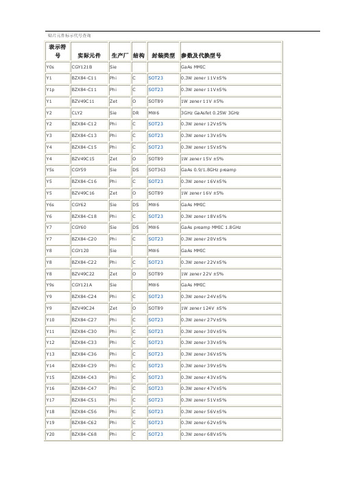
贴片元件标示代号查询
F
n-ch jfe t ultra low i/p Ig
Na t
F
n-ch jfe t ultra low i/p Ig
Na t
F
n-ch jfe t ultra low i/p Ig
Na t
F
n-ch jfe t sw/choppe r
Na t
F
n-ch jfe t sw/choppe r
Na t
Y5
BZV49C 16
Ze t
O
SOT89
1W zene r 16V ±5%
Y 6s
C GY62
Sie
DS MW 6
GaAs MMIC
Y6
BZX84 -C1 8
Phi
C
SOT23
0.3W zene r 18V±5%
Y7
C GY60
Sie
DS MW 6
GaAs preamp MMIC 1.8GHz
Y7
Y 83
BZX84 - A56
Phi
C
SOT23
0.3W zene r 56V ±1%
Y 84
BZX84 - A62
Phi
C
SOT23
0.3W zene r 62V ±1%
Y 85
BZX84 - A68
Phi
C
SOT23
0.3W zene r 68V ±1%
Y 86
BZX84 - A75
Phi
C
SOT23
I
SOD110
0.4W zene r 4.7V E12 ±5%
YW
BZX284-C 5V1 Phi
I
SOD110
西贝通达TDSV系列伺服驱动器使用手册

TDSV系列数字式交流伺服驱动器使用说明书北京西贝通达科技有限公司V1.2 Build 1522010年09月目录1概要 (1)2安全、正确使用规定 (2)2.1一般说明 (2)2.2防止触电伤害注意事项 (2)2.3防止损伤及设备损坏注意事项 (2)2.4防止火灾注意事项 (3)2.5其他注意事项 (3)2.5.1环境要求 (3)2.5.2安装及连接 (3)2.5.3运行 (4)3型号名称及技术规格 (6)3.1驱动器型号名称 (6)3.2技术规格 (6)4安装 (8)5信号与连接 (9)5.1信号定义 (9)5.1.1主回路强电端子 (9)5.1.2编码器反馈插头--CN1 (11)5.1.3控制信号插头—CN2 (12)5.1.4通讯插头—CN3 (17)5.2典型外部连接 (18)5.2.1主电路强电连接 (18)5.2.2模拟速度控制信号连接 (19)5.2.3模拟力矩控制信号连接 (20)5.2.4通讯接口信号连接 (20)6参数说明 (21)6.1参数设定及调整方法 (21)6.2参数的初始调整 (21)6.2.1电机参数的调整 (21)6.2.2运行方式参数的调整 (21)6.2.3控制回路调节参数的调整 (22)6.2.4专用功能参数的调整 (22)6.2.5通讯控制参数的调整 (22)6.3参数说明 (23)6.3.1电机参数 (23)6.3.2运行方式设定参数 (24)6.3.3运行指令参数 (31)6.3.4控制调节器参数 (35)6.3.6监视参数 (44)6.3.7专用功能设定参数 (49)6.3.7.1定位功能设定参数 (49)6.3.7.2摆动及切换变速比功能设定参数 (53)6.3.7.3模拟量刚性攻丝功能设定参数 (55)6.3.7.4模拟量铰孔功能设定参数 (56)6.3.7.5脉冲位置控制功能(C轴功能)设定参数 (57)6.3.8通讯参数 (59)6.4参数总表 (60)7操作面板 (68)7.1概述 (68)7.1.1指示灯状态及功能 (68)7.1.2按键功能 (68)7.1.3上电初始状态 (69)7.2数码管显示模式 (69)7.2.1数码管主菜单显示模式 (69)7.2.2参数管理模式子菜单显示 (69)7.2.3监控模式子菜单显示 (69)7.2.4辅助功能模式子菜单显示 (70)7.3参数管理模式 (71)7.3.1读取参数值 (71)7.3.2修改参数值 (71)7.3.3快速切换参数号 (72)7.4监控模式 (72)7.4.1切换监控参数 (72)7.4.2显示监控参数值 (73)7.5辅助功能模式 (73)7.5.1试运行电机 (73)7.5.2报警追踪 (74)7.5.3密码权限 (75)8TMS-WIN监控软件 (77)8.1概述 (77)8.2状态监控界面 (77)8.2.1驱动器工作状态 (78)8.2.2驱动器实时数据 (78)8.2.3电机控制 (79)8.2.4工具栏及状态栏 (80)8.2.5考机功能 (80)8.3参数界面 (81)8.3.1参数浏览 (81)8.3.2参数修改 (81)8.3.4I/O端口调试 (83)8.4图形界面 (84)8.4.1数据采样 (84)8.4.2图形设置 (86)8.4.3数据测量 (87)8.5用户权限 (87)8.6软件菜单 (88)9常见报警及处理方法 (91)10维护与检修 (93)10.1维护及检修内容 (93)10.2易损件更换 (94)10.3存储 (94)TDSV系列交流伺服驱动器使用说明书1概要感谢您购买TDSV系列交流伺服驱动器产品。
ASEMI肖特基二极管型号大全,找找MBR4045PT属于哪一类

编辑:GGASEMI肖特基二极管的型号众多,接下来所列型号主要以电流电压大小,分为大类,再以封装区分作为辅助分类。
ASEMI肖特基二极管型号大全,找找MBR4045PT属于哪一类1A~5A 20V~150V 肖特基二极管两者型号都在用SS封装:SS110 、SS14 。
10A 45V~200V 肖特基二极管采用TO-220AC封装的有:MBR10200AC、MBR10150AC、MBR10100AC、MBR1060AC、MBR1045AC、MBR1040AC采用TO-220封装的有:MBR1040FCT、MBR10200FCT、MBR10100FCT、MBR10150FCT、 MBR1040CT、MBR10200CT、MBR1040FCT、MBT1045FCT、 MBR1045CT、MBR1040CT、 MBR1045CT、MBR1060CT、MBR1060FCT、MBR10100CT、MBT10100FCT、MBR10150CT该封装有FCT和CT结尾的型号命名,区别于前者是塑封封装、后者是铁头封装。
采用TO-251封装的有:BD1045CT、BD1060CT、BD10100CT、BD10150CT、BD10200CT、BD1040CT采用TO-252封装的有:BD1040CS、BD1045CS、BD1060CS、BD10100CS、BD10150CS、 BD10200CS 采用TO-263封装的有:MBR10200DC、MBR1040DC、MBR1045DC、MBR1060DC、MBR10100DC、MBR10150DC20A 45V~200V肖特基二极管采用TO-220AC封装的有:MBR20200AC、MBR20150AC、MBR20100AC、MBR2060AC、 MR2045AC采用TO-251封装的有:BD2060CT、BD2045CT、BD20100CT、BD20150CT、BD20200CT、采用TO-252封装的有:BD20100CS、BD20150CS、BD20200CS、BD2045CS、BD2060CS采用TO-263封装的有:MBR2045DC、MBR2060DC、MBR20100DC、MBR20150DC、MBR20200DC采用TO-220封装的有:MBR2045CT、MBR2045FCT、MBR20200FCT、MBR2060CT、 MBR20100FCT、MBR2060FCT、MBR20100CT、MBR20100FCT、 MBR20150CT、MBR20150FCT、MBR20200CT、MBR20200FCT采用TO-247/3封装的有:MBR20200PT30A 45V~200V 肖特基二极管采用TO-247/3P封装的有:MBR3045PT、MBR3060PT、MBR30100PT、MBR30150PT、MBR30200PT采用TO-263封装的有:MBR30200DC、MBR3060DC、MBR30100DC、MBR30150DC、MBR3045DC采用TO-220封装的有:MBR3045CT、MBR3045FCT、MBR3060CT、MBR3060FCT、MBR30100CT、MBT30100FCT、MBR30150CT、MBR30150FCT、 MBR30200CT、MBR30200FCT 40A 45V~200V 肖特基二极管采用TO-263封装的有:MBR4045DC、MBR40200DC、MBR4060DC、MBR40100DC、MBR40150DC采用TO-247/3P封装的有:MBR40200PT、MBR4045PT、MBR4060PT、MBR40100PT、 MBR40150PT、采用TO-220封装的有:MBR4045FCT、MBR4045CT、MBR4060FCT、MB40100FCT、 MBR4060CT、MBR40100CT60A 45V~220V 肖特基二极管采用TO-247/3P封装的有:MBR6045PT、MBR6060PT、MBR60100PT、MBR60150PT、 MBR60200PT 10A~60A 20V~100V 肖特基二极管采用ITO-220AB封装的有:SBT10150UCT、SBT10100UCT、SBT1060UCT、SBT1045UCT、SBT10150VCT、SBT10100VCT、SBT1060VCT、SBT1045VCT、SBT30150UCT、SBT2045VCT、SBT2060VCT、SBT20100VCT、SBT20150VCT、SBT2045UCT、 SBT2060UCT、SBT20100UCT、 SBT20150UCT、SBT3045VCT、SBT3060VCT、SBT30100VCT、 SBT30150VCT、SBT3045UCT、SBT3060UCT、SBT30100UCT、SBT1045UFCT、SBT30100UFCT、SBT1060UFCT、SBT10150VFCT、SBT10100VFCT、SBT1060VFCT、SBT1045VFCT、SBT10100UFCT、SBT2045VFCT、SBT10150UFCT、 SBT2060VFCT、SBT20100VFCT、SBT20150VFCT、SBT2045UFCT、SBT2060UFCT、SBT20100UFCT、SBT20150UFCT、SBT3045VFCT、SBT3060VFCT、SBT30100VFCT、 SBT30150VFCT、SBT3045UFCT、SBT3060UFCT、SBT30150UFCT、SBT1045UFCT、 SB10100LCT、SB10150LCT、SB1045LFCT、SB1045LFCT、SB30100LFCT、 SB1060LFCT、SB30150LFCT、SB10100LFCT、SB2045LFCT、SB10150LFCT、SB2060LFCT、SB20100LFCT、SB3060LCT采用TO-220AB封装的有:SB1060LCT、SB30150LCT、SB30150LCT、SB10100LCT、SB2060LCT、SB10150LCT、SB20150LCT、SB3060LCT、SB30100LCT、SB1045LCT采用TO-277封装的有:10V45这款肖特基二极管型号是超低压降、贴片小封装的。
TXS0104E 4位双向多电压电平转换器说明书

适用于漏极开路和推挽应用的 TXS0104E 4 位双向多电压电平转换器1 特性•无需方向控制信号•最大数据速率–24Mbps(推挽)–2Mbps(开漏)•采用德州仪器 (TI) NanoFree™封装• A 端口支持 1.65V 至 3.6V 的电压,B 端口支持2.3V 至 5.5V 的电压 (V CCA≤ V CCB)•无需电源排序– V CCA或 V CCB均可优先斜升•闩锁性能超过 100mA,符合 JESD 78 II 类规范的要求•ESD 保护性能超过 JESD 22 规范要求–A 端口•2000V 人体放电模型 (A114-B)•200V 机器模型 (A115-A)•1000V 充电器件模型 (C101)–B 端口•15kV 人体放电模型 (A114-B)•200V 机器模型 (A115-A)•1000V 充电器件模型 (C101)•IEC 61000-4-2 ESD(B 端口)–±8kV 接触放电–±10kV 气隙放电2 应用•手持终端•智能手机•平板电脑•台式计算机3 说明这个 4 位同相转换器使用两个独立的可配置电源轨。
A 端口设计用于跟踪 V CCA。
V CCA支持从 1.65V 到 3.6V 范围内的任意电源电压。
V CCA必须低于或等于V CCB。
B 端口旨在用于跟踪 V CCB。
V CCB支持从 2.3V 到5.5V 范围内的任意电源电压。
这使得该器件可在 1.8V、2.5V、3.3V 和 5V 电压节点之间任意进行低压双向转换。
当输出使能端 (OE) 输入为低电平时,所有输出都被置于高阻抗状态。
TXS0104E 被设计成由 V CCA为 OE 输入电路供电。
为确保在加电或断电期间处于高阻抗状态,应将 OE 通过下拉电阻器接地;该电阻器的最小值取决于驱动器的拉电流能力。
(1)(1)如需了解所有可用封装,请参阅数据表末尾的可订购产品附录。
OutputVoltage(V)Input Voltage (V)C001N 沟道晶体管的传输特征内容1 特性...................................................................................12 应用...................................................................................13 说明...................................................................................14 修订历史记录.....................................................................25 引脚配置和功能.................................................................4引脚功能:ZXU/ NMN.......................................................4引脚功能:DSBGA...........................................................5引脚功能:D 、PW 或 RGY...............................................66 规格...................................................................................76.1 绝对最大额定值...........................................................76.2 ESD 等级....................................................................76.3 建议运行条件..............................................................86.4 热性能信息:ZXU 、YZT 和 NMN...............................86.5 热性能信息:D 、PW 和 RGY.....................................96.6 电气特性......................................................................96.7 时序要求:V CCA = 1.8V ± 0.15V...............................106.8 时序要求:V CCA = 2.5V ± 0.2V.................................106.9 时序要求:V CCA = 3.3V ± 0.3V.................................106.10 开关特性:V CCA = 1.8V ± 0.15V.............................116.11 开关特性:V CCA = 2.5V ± 0.2V...............................136.12 开关特性:V CCA = 3.3V ± 0.3V...............................156.13 典型特性..................................................................167 参数测量信息...................................................................177.1 负载电路.. (17)7.2 电压波形....................................................................188 详细说明..........................................................................198.1 概述...........................................................................198.2 功能方框图................................................................198.3 特性说明....................................................................208.4 器件功能模式............................................................209 应用和实现.......................................................................219.1 应用信息....................................................................219.2 典型应用....................................................................2110 电源相关建议.................................................................2311 布局................................................................................2411.1 布局布线指南...........................................................2411.2 布局示例..................................................................2412 器件和文档支持.............................................................2512.1 文档支持..................................................................2512.2 接收文档更新通知...................................................2512.3 社区资源..................................................................2512.4 商标.........................................................................2513 接收文档更新通知..........................................................2514 支持资源........................................................................2515 静电放电警告.................................................................2516 术语表............................................................................2517 机械、封装和可订购信息.. (25)4 修订历史记录注:以前版本的页码可能与当前版本的页码不同Changes from Revision H (May 2018) to Revision I (October 2020)Page•更新了整个文档的表、图和交叉参考的编号格式................................................................................................1•添加了 NMN 封装 12 引脚 nFBGA......................................................................................................................4Changes from Revision G (September 2017) to Revision H (May 2018)Page•更改了开关特性:V CCA = 3.3V ± 0.3V 表中最大数据速率的最大值..................................................................15Changes from Revision F (December 2014) to Revision G (September 2017)Page•更改了“器件信息”表........................................................................................................................................1•通篇删除了 GXU 引用.........................................................................................................................................4•在绝对最大额定值 中添加了结温........................................................................................................................7•重新编排了电气特性 ..........................................................................................................................................9•将电压转换基础知识 添加到“相关文档”........................................................................................................25•添加了接收文档更新通知 和社区资源 (25)Changes from Revision E (August 2013) to Revision F (December 2014)Page•添加了引脚配置和功能 部分、处理等级 表、特性说明 部分、器件功能模式、应用和实施 部分、电源相关建议 部分、布局 部分、器件和文档支持 部分以及机械、封装和可订购信息 部分......................................................1•从“绝对最大额定值”表中删除了封装热阻信息,并将其添加到“热性能信息”表中将 T stg 行移到了新的“处理额定值”表中...................................................................................................................................................7•将第一个开关特性表中最后 2 行的“最小值最大值”中的最大值 24 和最大值 2 更改到最小值列. (11)TXS0104EZHCSI61I – JUNE 2006 – REVISED OCTOBER 2020Changes from Revision D (May 2008) to Revision E (August 2013)Page•删除了订购表 (1)TXS0104EZHCSI61I – JUNE 2006 – REVISED OCTOBER 20205 引脚配置和功能图 5-1. ZXU 封装顶视图图 5-2. NMN 顶视图引脚功能:ZXU/ NMNTXS0104EZHCSI61I – JUNE 2006 – REVISED OCTOBER 2020图 5-3. YZT 封装 12 引脚 DSBGA 顶视图引脚功能:DSBGATXS0104EZHCSI61I – JUNE 2006 – REVISED OCTOBER 20201147823456131211109B1B2B3B4NCA1A2A3A4NCO EV G N DC C BV C C ANC - 无内部连接图 5-4. RGY 封装 14 引脚 VQFN 顶视图NC - 无内部连接图 5-5. D 和 PW 封装 14 引脚 SOIC 和 TSSOP 顶视图引脚功能:D 、PW 或 RGYTXS0104EZHCSI61I – JUNE 2006 – REVISED OCTOBER 20206 规格6.1 绝对最大额定值(1)(1)应力超出绝对最大额定值 下所列的值可能会对器件造成损坏。
广州唯创电子 WTB 系列语音芯片说明书
WTB系列语音芯片使用说明书目录1、WTB芯片特征 (3)2、应用范围 (3)3、WTB系列语音芯片选型 (3)4、WTB系列语音芯片应用方框图 (4)5、封装示意图 (4)6、管脚描述 (5)6.1、WTB015/031-16P封装引脚对应表 (5)6.2、WTB015-18S封装引脚对应表 (5)6.3、WTB031-18S封装引脚对应表 (6)6.4、WTB084-20SS/20P封装引脚对应表 (7)7、电器参数 (8)8、环境绝对极限参数 (8)9、定义IO口 (9)10、控制模式 (9)10.1、按键控制模式 (9)10.1.1、脉冲可重复触发 (9)10.1.2、脉冲不可重复触发 (9)10.1.3、电平保持可循环触发 (10)10.1.4、电平保持不可循环触发 (10)10.1.5、下一曲触发 (10)10.1.6、上一曲触发 (10)10.1.7、播放/停止触发 (11)10.1.8、播放/暂停触发 (11)10.2、一线串口控制模式 (11)10.2.1、端口分配表 (11)10.2.2、发送8位数据控制形式语音地址对应关系 (12)10.2.3、发送8位数据控制形式控制时序图 (12)10.2.4、发送16位数据控制形式语音地址对应关系 (12)10.2.5、发送16位数据控制形式控制时序图 (13)10.3、三线串口控制模式 (13)10.3.1、端口分配方式 (13)10.3.2、语音地址对应关系 (13)10.3.3、三线串口控制时序 (14)11、典型应用电路 (14)11.1、WTB015/031-16P (14)11.1.1、WTB015/031-16P按键控制(PWM输出)应用电路 (14)11.1.2、WTB015/031-16P按键控制(DAC输出)应用电路 (15)11.1.3、WTB015/031-16P一线串口控制(PWM输出)应用电路 (15)11.1.4、WTB015/031-16P一线串口控制(DAC输出)应用电路 (15)11.1.5、WTB015/031-16P三线串口控制(PWM输出)应用电路 (16)11.1.6、WTB015/031-16P三线串口控制(DAC输出)应用电路 (16)11.2、WTB015/031-18S (16)11.2.1、WTB015/031-18S按键控制(PWM输出)应用电路 (16)11.2.2、WTB031-18S按键控制(DAC输出)应用电路 (17)11.2.3、WTB015/031-18S一线串口控制(PWM输出)应用电路 (17)11.2.4、WTB015/031-18S一线串口控制(DAC输出)应用电路 (17)11.2.5、WTB015/031-18S三线串口(PWM输出)应用电路 (18)11.2.6、WTB015/031-18S三线串口(DAC输出)应用电路 (18)11.3、WTB084-20SS/20P (19)11.3.1、WTB084-20SS/20P按键控制(PWM输出)应用电路 (19)11.3.2、WTB084-20SS/20P按键控制(DAC输出)应用电路 (19)11.3.3、WTB084-20SS/20P一线串口(PWM输出)应用电路 (19)11.3.4、WTB084-20SS/20P一线串口(DAC输出)应用电路 (20)11.3.5、WTB084-20SS/20P三线串口(PWM输出)应用电路 (20)11.3.6、WTB084-20SS/20P三线串口(DAC输出)应用电路 (20)12、应用范例电路 (21)12.1、电动车应用电路 (21)12.2、定时药盒应用电路 (22)13、控制程序范例 (22)13.1、一线串口(发送8位数据控制形式)控制程序范例 (22)13.2、一线串口(发送16位数据控制形式)控制程序范例 (24)13.3、三线串口控制程序范例 (27)14、封装尺寸 (29)14.1、WTB015/031-16P封装尺寸 (29)14.2、WTB015/031-18S封装尺寸 (30)15、货源信息 (31)16、说明书版本记录 (31)1、WTB芯片特征WTB语音芯片是一款低成本OTP语音芯片;工业级性能,确保产品在多种场合下正常工作;内置音频合成器的4位微型语音处理器及4位数字逻辑运算器;WTB语音芯片完备的内部资源包括EPROM、RAM和I/O端口等;可定义多路输入端和输出端;随意定义控制输入端触发功能;自动休眠功能,有效降低功耗;支持WAV音频和两通道MIDI播放;可工作于4MHz和8MHz两种震荡模式,不同模式下的音频最高采样率分别为14KHz和28KHz;WTB系列语音芯片包括WTB015、WTB031、WTB084、WTB170,其存储时间分别为15秒、31秒、84秒、170秒,目前库存有WTB015、WTB031和WTB084三种;可加载128段语音进行控制播放;单芯片方案,可掩膜投产,降低批量生产成本;支持9bit D/A和8bit PWM输出;工作电压:DC2.2V~5.5V。
启珑微电子产品手册说明书

产品手册PRODUCT MANUAL(北京︶有限公司并一直致力于为工业智能控制、医疗设备、轨道交通、智能交通以及智能家居等领域提供更优质的产品与服务。
公司具有深厚的文化底蕴,由多位有欧美留学、工作经历的归国人员创办,坚实的理论功底和丰富的芯片设计经验奠定了启珑微电子的高起点和高水准,并迅速成长为业内具有自主知识产权的中国IC设计品牌之一。
产品手册01序号产品型号封装形式产品概述兼容型号1CLM811HST-AXC TQFP-48SL811HST-AXC 2CLCP82C55AZ DIP-40CP82C55AZ 3CLIP82C55AZ DIP-40IP82C55AZ 4CLCS82C55AZ PLCC-44CS82C55AZ 5CLIS82C55AZ PLCC-44IS82C55AZ 6CLCQ82C55AZ MQFP-44CQ82C55AZ 7CLIQ82C55AZ MQFP-44IQ82C55AZ 8CLID82C55AZ DIP-40ID82C55A 9CLMD82C55A/B DIP-40MD82C55A/B 10CLMD82C55QA DIP-40MD82C55QA 11CLM65HVD230D SOIC-8SN65HVD230D 12CLM65HVD230QD SOIC-8SN65HVD230QD 13CLM65HVD231D SOIC-8SN65HVD231D 14CLM65HVD231QD SOIC-8SN65HVD231QD 15CLM65HVD232D SOIC-8SN65HVD232D 16CLM65HVD232QD SOIC-8SN65HVD232QD 17CLM65HVD233D SOIC-8具有待机模式和环回功能的 3.3V SN65HVD233D 18CLM65HVD233HD SOIC-8具有待机模式和环回功能的 3.3V SN65HVD233HD 19CLM65HVD233QDRQ1SOIC-8具有待机模式和环回功能的 3.3V SN65HVD233QDRQ120CLM65HVD233MDREP SOIC-8具有待机模式和环回功能的 3.3V SN65HVD233MDREP产品手册02序号产品型号封装形式产品概述兼容型号21CLM65HVD234D SOIC-8SN65HVD234D 22CLM65HVD234QDRQ1SOIC-8SN65HVD234QDRQ123CLM65HVD235D SOIC-8SN65HVD235D 24CLM65HVD235QDRQ1SOIC-8SN65HVD235QDRQ125CLM75176BPS SOIC-8SN75176BPSR 26CLM75176BDR SOIC-8SN75176BDR 27CLM75176ADR SOIC-8SN75176ADR 28CLM75176AP DIP-8SN75176AP 29CLM76176BP DIP-8SN75176BP 30CLM75179BPS SOIC-8SN75179BPS 31CLM75179BDR SOIC-8SN75179BDR 32CLM75179AP DIP-8SN75179AP 33CLM75179BP DIP-8SN75179BP 34CLM65HVD08D SOIC-8SN65HVD08D 35CLM65HVD08P DIP-8SN65HVD08P 36CLM65HVD75D SOIC-8具有IEC ESD保护功能和20Mbps的SN65HVD75D 37CLM65HVD75DGK VSSOIC-8具有IEC ESD保护功能和20Mbps的SN65HVD75DGK 38CLM65HVD75DRBT VDFN-8具有IEC ESD保护功能和20Mbps的SN65HVD75DRBT 39CLM3085CPA+DIP-8(10Mbps)、限摆率RS-485/MAX3085CPA+40CLM3085EPA+DIP-8(10Mbps)、限摆率RS-485/MAX3085EPA+产品手册03序号产品型号封装形式产品概述兼容型号41CLM3085EEPA DIP-8(10Mbps)、限摆率RS-485/MAX3085EEPA 42CLM3085CSA+T SOIC-8(10Mbps)、限摆率RS-485/MAX3085CSA+43CLM3085ECSA+T MSOIC-8(10Mbps)、限摆率RS-485/MAX3085ECSA+T 44CLM3085ESA+T SOIC-8(10Mbps)、限摆率RS-485/MAX3085ESA+45CLM3085EESA+T SOIC-8(10Mbps)、限摆率RS-485/MAX3085EESA+46CLM3088CSA+T SOIC-8MAX3088CSA+T 47CLM3088ECSA+T SOIC-8MAX3088ECSA+T 48CLM3088ESA+T SOIC-8MAX3088ESA+T 49CLM3088EESA+T SOIC-8MAX3088EESA+T 50CLM3088CPA+DIP-8MAX3088CPA+51CLM3088ECPA+DIP-8MAX3088ECPA+52CLM3088EPA+DIP-8MAX3088EPA+53CLM3088EEPA+DIP-8MAX3088EEPA+54CLM485CPA+DIP-8低功耗、限摆率、RS-485/RS-422MAX485CPA+55CLM485ECPA+DIP-8低功耗、限摆率、RS-485/RS-422MAX485ECPA+56CLM485EPA+DIP-8低功耗、限摆率、RS-485/RS-422MAX485EPA+57CLM485EEPA+DIP-8低功耗、限摆率、RS-485/RS-422MAX485EEPA+58CLM485CSA+SOIC-8低功耗、限摆率、RS-485/RS-422MAX485CSA+59CLM485ESA+SOIC-8低功耗、限摆率、RS-485/RS-422MAX485ESA+60CLM485EESA+SOIC-8低功耗、限摆率、RS-485/RS-422MAX485EESA+产品手册04序号产品型号封装形式产品概述兼容型号61CLM3490CSA+SOIC-8 3.3V供电、10Mbps、限摆率、真MAX3490CSA+62CLM3490ECSA+SOIC-8 3.3V供电、10Mbps、限摆率、真MAX3490ESA+63CLM3490ESA+SOIC-8 3.3V供电、10Mbps、限摆率、真MAX3490ESA+64CLM3490EESA+SOIC-8 3.3V供电、10Mbps、限摆率、真MAX3490EESA+65CLM3491CSD SOP-14 3.3V供电、10Mbps、限摆率、真MAX3491CSD+66CLM3491ECSD+SOP-14 3.3V供电、10Mbps、限摆率、真MAX3491ECSD+67CLM3491ESD+SOP-14 3.3V供电、10Mbps、限摆率、真MAX3491ESD+68CLM3491EESD+SOP-14 3.3V供电、10Mbps、限摆率、真MAX3491EESD+69CLM490CSA+SOIC-8低功耗、限摆率、RS-485/RS-422MAX490CSA+70CLM490ECSA+SOIC-8低功耗、限摆率、RS-485/RS-422MAX490ECSA+71CLM490ESA+SOIC-8低功耗、限摆率、RS-485/RS-422MAX490ESA+72CLM490EESA+SOIC-8低功耗、限摆率、RS-485/RS-422MAX490EESA+73CLM490CPA+DIP-8低功耗、限摆率、RS-485/RS-422MAX490CPA+74CLM490ECPA+DIP-8低功耗、限摆率、RS-485/RS-422MAX490ECPA+75CLM490EPA+DIP-8低功耗、限摆率、RS-485/RS-422MAX490EPA+76CLM490EEPA+DIP-8低功耗、限摆率、RS-485/RS-422MAX490EEPA+77CLM488CSA+SOIC-8低功耗、限摆率、RS-485/RS-422MAX488CSA+78CLM488ECSA+SOIC-8低功耗、限摆率、RS-485/RS-422MAX488ECSA+79CLM488ESA+SOIC-8低功耗、限摆率、RS-485/RS-422MAX488ESA+80CLM488EESA+SOIC-8低功耗、限摆率、RS-485/RS-422MAX488EESA+产品手册序号产品型号封装形式产品概述兼容型号81CLM488CPA+DIP-8MAX488CPA+82CLM488ECPA+DIP-8MAX488ECPA+83CLM488EPA+DIP-8MAX488EPA+84CLM488EEPA+DIP-8MAX488EEPA+85CLM232CSE SOIC-16MAX232CSE+T86CLM232ECSE SOIC-16MAX232ECSE+87CLM232ESE SOIC-16MAX232ESE+T88CLM232EESE SOIC-16MAX232EESE+T89CLM232CPE DIP-16MAX232CPE+90CLM232ECPE DIP-16MAX232ECPE+91CLM232EPE DIP-16MAX232EPE+92CLM232EEPE DIP-16MAX232EEPE+93CLM232CWE SOIC-16MAX232CWE+T94CLM232ECWE SOIC-16MAX232ECWE+T95CLM232EWE SOIC-16MAX232EWE+T96CLM232EEWE SOIC-16MAX232EEWE+T97CLM232ACWE SOIC-16MAX232ACWE+T98CLM232AEWE SOIC-16MAX232AEWE+99CLM3232CSE SOIC-16MAX3232CSE+T 100CLM3232ECSE SOIC-16MAX3232ECSE+T05产品手册06序号产品型号封装形式产品概述兼容型号101CLM3232ESE SOIC-16MAX3232ESE+T 102CLM3232EESE SOIC-16MAX3232EESE+T 103CLM1302S SOIC-8DS1302S+T&R 104CLM1302SN+SOIC-8DS1302SN+T&R 105CLM1302Z+T SOIC-8DS1302Z+T&R 106CLM1302ZN+SOIC-8DS1302ZN+T&R 107CLM1302+DIP-8DS1302+108CLM1302N+DIP-8DS1302N+109CLM307Z+SOIC-8DS1307Z+T&R 110CLM1307ZN+SOIC-8DS1307ZN+T&R 111CLM1307+DIP-8DS1307+112CLM1307N+DIP-8DS1307N+113CLM4717EUB+MSOP-10拟开关MAX4717EUB+114CLM231N/NOPB DIP-8LM231N/NOPB 115CLM231AN/NOPB DIP-8LM231AN/NOPB 116CLM331N/NOPB DIP-8LM331N/NOPB 117CLM331AN/NOPB DIP-8LM331AN/NOPB 118CLM298N Multiwatt-15L298N 119CLM298P POWERSO-20L298P 120CLM2543CDW SOIC-20TLC2543CDW产品手册07序号产品型号封装形式产品概述兼容型号121CLM2543IDW SOIC-20TLC2543IDW 122CLM2543CDB SSOP-20TLC2543CDB 123CLM2543IDB SSOP-20TLC2543IDB 124CLM2543CN DIP-20TLC2543CN 125CLM2543IN DIP-20TLC2543IN 126CLM1543CDW SOIC-20TLC1543CDW 127CLM1543IDW SOIC-20TLC1543IDW 128CLM1543CN DIP-20TLC1543CN 129CLM1543IN DIP-20TLC1543IN 130CLM5615CDGK VSSOIC-8趋稳时间为12.5us并具备上电复位功能的10位、单通道、低功耗DAC TLC5615CDGK 131CLM5615IDGK VSSOIC-8趋稳时间为12.5us并具备上电复位功能的10位、单通道、低功耗DAC TLC5615IGGK 132CLM5615CD SOIC-8趋稳时间为12.5us并具备上电复位功能的10位、单通道、低功耗DAC TLC5615CD 133CLM5615ID SOIC-8趋稳时间为12.5us并具备上电复位功能的10位、单通道、低功耗DAC TLC5615ID 134CLM5615CP DIP-8趋稳时间为12.5us并具备上电复位功能的10位、单通道、低功耗DAC TLC5615CP 135CLM5615IP DIP-8趋稳时间为12.5us并具备上电复位功能的10位、单通道、低功耗DAC TLC5615IP 136CLM3616-00SOP-14IW3616-00137CLM3616-01SOP-14IW3616-01138CLM3617-00SOP-14IW3617-00139CLM3617-01SOP-14IW3617-01140CLM3630-00SOP-14IW3630-00产品手册序号产品型号封装形式产品概述兼容型号141CLM1100-0001BGA-128ASIC从站控制ET1100-0001142CLM1100-0002BGA-128ASIC从站控制ET1100-0002143CLM1100-0003BGA-128ASIC从站控制ET1100-0003144CLM1200-0001QFN-48ASIC从站控制ET1200-0001145CLM1200-0002QFN-48ASIC从站控制ET1200-0002146CLM1200-0003QFN-48ASIC从站控制ET1200-0003147CLM8656ARZ SOIC-8AD8656ARZ148CLM8656ARMZ MSOIC-8AD8656ARMZ149CLM1040T/CM,118SOIC-8TJA1040T/CM,118 150CLM1042T/CM,118SOIC-8TJA1042T/CM,118 151CLM1050T/CM,118SOIC-8TJA1050T/CM,118 152CLM1051T/CM,118SOIC-8TJA1051T/CM,118 153CLM82C250T/YM SOIC-8PCA82C250T/YM 154CLM82C251T/YM SOIC-8PCA82C251T/YM 155CLMEE80C196KC20PLCC-68EE80C196KC20 156CLMEN80C196KC20PLCC-68EN80C196KC20 157CLMN80C196KC20PLCC-68N80C196KC20 158CLMTN80C196KC20PLCC-68TN80C196KC20 159CLMEE87C196KC20PLCC-68EE87C196KC20 160CLMEN87C196KC20PLCC-68EN87C196KC2008产品手册09序号产品型号封装形式产品概述兼容型号161CLMN87C196KC20PLCC-68N87C196KC20162CLMTN87C196KC20PLCC-68TN87C196KC20163CLM8051F020-GQ TQFP-100C8051F020-GQ 164CLM8051F021-GQ TQFP-64C8051F021-GQ 165CLM8051F330-GM VFQFN-20C8051F330-GM 166CLM8051F500-IQ TQFP-48C8051F500-IQ 167CLM8051F500-IM VFQFN-48C8051F500-IM 168CLM8051F502-IQ LQFP-32C8051F502-IQ 169CLM8051F502-IM QFN-32C8051F502-IM170CLM08D1500CIYB/NOPB HLQFP-128ADC08D1500CIYB/NOPB 171CLM083000CIYB/NOPB HLQFP-128ADCADC083000CIYB/NOPB 172CLM10AQ190AVTPY EBGA-38010位5GSPS ADC EV10AQ190AVTPY 173CLM9680BCPZ-1250LFCSP-64双通道14位1GSPS ADC AD9680BCPZ-1250174CLM9739BBCZ BGA-16014位、2.5 GSPS、RF数模AD9739BBCZ 175CLM9779ABSVZ TQFP-100双通道16位1GSPS DAC AD9779ABSVZ 176CLM12DS130AVZPY FPBGA-19612位3GSPS DAC EV12DS130AVZPY 177CLM12DS460AVZP FPBGA-19612位6.4GSPS DAC EV12DS460AVZP 178CLM9434BCPZ-370LFCSP-5612位370MSPS ADC AD9434BCPZ-370179CLM9434BCPZ-500LFCSP-5612位500MSPS ADC AD9434BCPZ-500180CLM4149IRGZTVQFN-4814位250MSPS ADCADS4149IRGZT产品手册10序号产品型号封装形式产品概述兼容型号181CLM9467BCPZ-200LFCSP-7216位200MSPS ADC AD9467BCPZ-200182CLM9467BCPZ-250LFCSP-7216位250MSPS ADC AD9467BCPZ-250183CLM9656BCPZ-125LFCSP-56四通道16位125MSPS ADC AD9656BCPZ-125184CLM9245BCPZ-40LFCSP-3214位40MSPS ADC AD9245BCPZ-40185CLM9245BCPZ-65LFCSP-3214位65MSPS ADC AD9245BCPZ-80186CLM9245BCPZ-80LFCSP-3214位80MSPS ADC AD9245BCPZ-80187CLM9783BCPZ LFCSP-72双通道16位500MSPS DAC AD9783BCPZ 188CLM7656BSTZ-REEL LQFP-64六通道16位250KSPS ADC AD7656BSTZ-REEL 189CLM7960BCPZLFCSP-3218位2MSPS ADC AD7960BCPZ190CLM128S102CIMTX/NOPB TSSOP-1612位1MSPS ADC ADC128S102CIMTX/NOPB 191CLM5638IDR SOIC-8DACTLV5638IDR 192CLM7606BSTZ LQFP-64AD7606BSTZ 193CLM9625BBPZ-2.5BGA-19612位2.6GSPS ADC AD9625BBPZ-2.5194CLM9164BBCZ BGA-16516位12GSPS DAC AD9164BBCZ 195CLM9154BCPZ LFCSP-88四通道16位2.4GSPS DAC AD9154BCPZ 196CLM2160IUK#PBF QFN-4816位25MSPS ADC LTC2160IUK#PBF 197CLM9652BBCZ-310BGA-144双通道16位310MSPS ADC AD9652BBCZ-310198CLM7779ACPZ-RL LFCSP-6424位16KSPS ADC AD7779ACPZ-RL 199CLM9208BBPZ-3000BGA-196双通道14位3GSPS ADCAD9208BBPZ-3000200CLM320VC33PGE120LQFP-144TMS320VC33PGE120产品手册序号产品型号封装形式产品概述兼容型号201CLM320VC33PGEA120LQFP-144TMS320VC33PGEA120 202CLM320VC33PGE150LQFP-144TMS320VC33PGE150203CLM320VC5402PGE100LQFP-144TMS320VC5402PGE100 204CLM320F28335PGFA LQFP-176TMS320F28335PGFA205CLM320LF2406APZA LQFP-100TMS320LF2406APZA206CLM320LF2406APZS LQFP-100TMS320LF2406APZS207CLM320LF2407APGES LQFP-144TMS320LF2407APGES208CLM320LF2407APGEA LQFP-144TMS320LF2407APGEA 209CLM320C6713BPYP200HLQFP-208TMS320C6713BPYP200 210CLM320C6713BZDP225BGA-272TMS320C6713BZDP225 211CLM320C6713BGDP225BGA-272TMS320C6713BGDP225 212CLM320C6713BZDP300BGA-272TMS320C6713BZDP300 213CLM320C6713BGDG300BGA-272TMS320C6713BGDP30011邮箱:*******************。
leuze electronic GSU 14C说明书

leuze electronic GSU 14C说明书物理数据口宽 4mm 口深 68mm 标签长度≥ 5mm 标签宽度≥ 10mm 标签间隙≥ 2mm 传送带速度≤ 240m/min (4m/s) 传送带速度≤ 50m/min(0.83m/s) 典型响应时间≤ 200 µs 重复性 1)1)取决于传送带速度、标签长度和标签之间的间距± 0.2mm 启动前的延迟≤ 300ms 符合IEC 60947-5-2标准电气数据工作电压UB 2) 2)对于UL应用:仅适用于NEC规定的2级电路中12VDC (-5%) ...30VDC (包括残余纹波) 残余纹波≤UB的15% 开路电流≤80mA 开关输出 3) .../663)推挽式开关输出端不得并列连接2个推挽式开关输出针脚4:PNP光开关,NPN暗开关针脚2:PNP暗开关,NPN光开关 (66)2个推挽式开关输出针脚4:PNP暗开关,NPN光开关针脚2:PNP 光开关,NPN暗开关 .../6 1个推挽式开关输出针脚4:PNP光开关,NPN暗开关 .../6D 1个推挽式开关输出针脚4。
PNP暗开关,NPN明开关警告输出2) 1个推挽式开关输出引脚2:低电平有效(正常操作高电平,事件情况低电平)功能开关输出 IGSU明/暗开关,可调信号电压高/低≥(UB-2V)/≤2V 输出电流≤100mA 容性负载≤0. 5µF 指示器绿色LED准备就绪绿色LED,闪烁的示教激活黄色LED开关点在标签间隙红色LED示教错误/功能错误机械数据外壳压铸锌,涂漆颜色红色/黑色重量 270克连接方式M12连接器,5针脚环境数据环境温度(操作/储存)0°C ... +60°C/-40°C ... +70°C 保护电路 4) 4) 1=极性反转保护,2=所有输出的短路保护1, 2VDE 安全等级 III 保护等级 IP 65 适用标准 IEC 60947-5-2 认证 UL 508, C22.2 No.14-13 2) 5)5) 这些接近开关在现场安装时,应与额定为30V、0.5A的UL认证电缆组件一起使用,或与之相当(类别:CYJV/CYJV7或PVVA/PVVA7)。
FPGA可编程逻辑器件芯片XCZU15EG-2FFVB1156E中文规格书

Zynq UltraScale+ MPSoCsA comprehensive device family, Zynq UltraScale+ MPSoCs offer single-chip, all programmable,heterogeneous multiprocessors that provide designers with software, hardware, interconnect, power, security, and I/O programmability. The range of devices in the Zynq UltraScale+MPSoC family allows designers to target cost-sensitive as well as high-performance applications from a single platform using industry-standard tools. While each Zynq UltraScale+MPSoC contains the same PS, the PL, Video hard blocks, and I/O resources vary between the devices.•Automotive: Driver assistance, driver information, and infotainment•Wireless Communications: Support for multiple spectral bands and smart antennas•Wired Communications: Multiple wired communications standards and context-aware network services •Data Centers: Software Defined Networks (SDN), data pre-processing, and analytics •Smarter Vision: Evolving video-processing algorithms, object detection, and analytics•Connected Control/M2M: Flexible/adaptable manufacturing, factory throughput, quality, and safetyThe UltraScale MPSoC architecture provides processor scalability from 32 to 64 bits with support for virtualization, the combination of soft and hard engines for real-time control, graphics/video processing, waveform and packet processing, next-generation interconnect and memory, advanced powermanagement, and technology enhancements that deliver multi-level security, safety, and reliability. Xilinx offers a large number of soft IP for the Zynq UltraScale+MPSoC family. Stand-alone and Linux device drivers are available for the peripherals in the PS and the PL. Xilinx’s Vivado® Design Suite, SDK™, and PetaLinux development environments enable rapid product development for software, hardware, and systems engineers. The Arm-based PS also brings a broad range of third-party tools and IP providers in combination with Xilinx's existing PL ecosystem.The Zynq UltraScale+MPSoC family delivers unprecedented processing, I/O, and memory bandwidth in the form of an optimized mix of heterogeneous processing engines embedded in a next-generation, high-performance, on-chip interconnect with appropriate on-chip memory subsystems. Theheterogeneous processing and programmable engines, which are optimized for different application tasks, enable the Zynq UltraScale+ MPSoCs to deliver the extensive performance and efficiency required to address next-generation smarter systems while retaining backwards compatibility with the original Zynq-7000 All Programmable SoC family. The UltraScale MPSoC architecture also incorporates multiple levels of security, increased safety, and advanced power management, which are critical requirements of next-generation smarter systems. Xilinx’s embedded UltraFast™ design methodology fully exploits the Table 7:Zynq UltraScale+ MPSoC Device FeaturesCG DevicesEG DevicesEV DevicesAPU Dual-core Arm Cortex-A53Quad-core Arm Cortex-A53Quad-core Arm Cortex-A53RPU Dual-core Arm Cortex-R5Dual-core Arm Cortex-R5Dual-core Arm Cortex-R5GPU –Mali-400MP2Mali-400MP2VCU––H.264/H.265找FPGA 和CPLD 可编程逻辑器件,上深圳宇航军工半导体有限公司ASIC-class capabilities afforded by the UltraScale MPSoC architecture while supporting rapid system development.The inclusion of an application processor enables high-level operating system support, e.g., Linux. Other standard operating systems used with the Cortex-A53 processor are also available for theZynq UltraScale+MPSoC family. The PS and the PL are on separate power domains, enabling users to power down the PL for power management if required. The processors in the PS always boot first, allowing a software centric approach for PL configuration. PL configuration is managed by software running on the CPU, so it boots similar to an ASSP.Programmable LogicThis section covers the information about blocks in the Programmable Logic (PL).Device LayoutUltraScale architecture-based devices are arranged in a column-and-grid layout. Columns of resources are combined in different ratios to provide the optimum capability for the device density, target market or application, and device cost. At the core of UltraScale+MPSoCs is the processing system that displaces some of the full or partial columns of programmable logic resources. Figure 1 shows a device-level view with resources grouped together. For simplicity, certain resources such as the processing system, integrated blocks for PCIe, configuration logic, and System Monitor are not shown.Resources within the device are divided into segmented clock regions. The height of a clock region is 60CLBs. A bank of 52 I/Os, 24 DSP slices, 12 block RAMs, or 4 transceiver channels also matches the height of a clock region. The width of a clock region is essentially the same in all cases, regardless of device size or the mix of resources in the region, enabling repeatable timing results. Each segmented clock region contains vertical and horizontal clockrouting that span its full height and width. These horizontal and vertical clock routes can be segmented at the clock region boundary to provide a flexible, high-performance, low-power clock distribution architecture. Figure 2 is a representation of a device divided into regions.Figure 1:Device with Columnar ResourcesFigure 2:Column-Based Device Divided into Clock RegionsHigh-Speed Serial TransceiversUltra-fast serial data transmission between devices on the same PCB, over backplanes, and across even longer distances is becoming increasingly important for scaling to 100Gb/s and 400Gb/s line cards. Specialized dedicated on-chip circuitry and differential I/O capable of coping with the signal integrity issues are required at these high data rates.Three types of transceivers are used in Zynq UltraScale+ MPSoCs: GTH, GTY, and PS-GTR. All transceivers are arranged in groups of four, known as a transceiver Quad. Each serial transceiver is a combined transmitter and receiver. Table 10 compares the available transceivers.The following information in this section pertains to the GTH and GTY only.The serial transmitter and receiver are independent circuits that use an advanced phase-locked loop (PLL) architecture to multiply the reference frequency input by certain programmable numbers between 4 and 25 to become the bit-serial data clock. Each transceiver has a large number of user-definable features and parameters. All of these can be defined during device configuration, and many can also be modified during operation.Table 10:Transceiver InformationZynq UltraScale+ MPSoCsType PS-GTRGTH GTY Qty40–440–28Max. Data Rate 6.0Gb/s 16.3Gb/s 32.75Gb/s Min. Data Rate1.25Gb/s0.5Gb/s0.5Gb/sApplications•PCIe Gen2•USB•Ethernet•Backplane •HMC•100G+Optics •Chip-to-Chip •25G+Backplane •HMC。
- 1、下载文档前请自行甄别文档内容的完整性,平台不提供额外的编辑、内容补充、找答案等附加服务。
- 2、"仅部分预览"的文档,不可在线预览部分如存在完整性等问题,可反馈申请退款(可完整预览的文档不适用该条件!)。
- 3、如文档侵犯您的权益,请联系客服反馈,我们会尽快为您处理(人工客服工作时间:9:00-18:30)。
Independent Clock HOTLink II™Serializer and Reclocking DeserializerCYV15G0104TRBFeatures•Second-generation HOTLink ® technology•Compliant to SMPTE 292M and SMPTE 259M video standards•Single channel video serializer plus single channel video reclocking deserializer—195- to 1500-Mbps serial data signaling rate —Simultaneous operation at different signaling rates•Supports reception of either 1.485 or 1.485/1.001 Gbps data rate with the same training clock•Internal phase-locked loops (PLLs) with no external PLL components•Supports half-rate and full-rate clocking•Selectable differential PECL-compatible serial inputs—Internal DC-restoration•Redundant differential PECL-compatible serial outputs —No external bias resistors required —Internal source termination —Signaling-rate controlled edge-rates •Synchronous LVTTL parallel interface •JTAG boundary scan•Built-In Self-Test (BIST) for at-speed link testing •Link Quality Indicator —Analog signal detect —Digital signal detect•Low-power 1.8W @ 3.3V typical •Single 3.3V supply•Thermally enhanced BGA•Pb-Free package option available •0.25μ BiCMOS technologyFunctional DescriptionThe CYV15G0104TRB Independent Clock HOTLink II™Serializer and Reclocking Deserializer is a point-to-point or point-to-multipoint communications building block enabling transfer of data over a variety of high-speed serial links including SMPTE 292M and SMPTE 259M video applications.It supports signaling rates in the range of 195 to 1500 Mbps per serial link. The transmit and receive channels are independent and can operate simultaneously at different rates. The transmit channel accepts 10-bit parallel characters in an Input Register and converts them to serial data. The receive channel accepts serial data and converts it to 10-bit parallel characters and presents these characters to an Output Register. The received serial data can also be reclocked and retransmitted through the reclocker serial outputs. Figure 1illustrates typical connections between independent video co-processors and corresponding CYV15G0104TRB chips.The CYV15G0104TRB satisfies the SMPTE 259M and SMPTE 292M compliance as per SMPTE EG34-1999 Patho-logical Test Requirements.As a second-generation HOTLink device, the CYV15G0104TRB extends the HOTLink family with enhanced levels of integration and faster data rates, while maintaining serial-link compatibility (data and BIST) with other HOTLink devices. The transmit (TX) channel of the CYV15G0104TRB HOTLink II device accepts scrambled 10-bit transmission characters. These characters are serialized and output from dual Positive ECL (PECL) compatible differential trans-mission-line drivers at a bit-rate of either 10- or 20-times the input reference clock for that channel.The receive (RX) channel of the CYV15G0104TRB HOTLink II device accepts a serial bit-stream from one of two selectable PECL-compatible differential line receivers, and using a completely integrated Clock and Data Recovery PLL, recovers the timing information necessary for data reconstruction. The recovered bit-stream is reclocked and retransmitted through the reclocker serial outputs. Also, the recovered serial data is deserialized and presented to the destination host system.Figure 1. HOTLink II™ System ConnectionsV i d e o C o p r o c e s s o r1010Video Coprocessor1010Serial LinksIndependentCYV15G0104TRBIndependent DeviceDeviceChannelCYV15G0104TRBChannelReclocked OutputReclocked OutputCYV15G0104TRBThe transmit and receive channels contain an independent BIST pattern generator and checker, respectively. This BIST hardware allows at-speed testing of the high-speed serial data paths in each transmit and receive section, and across the interconnecting links.The CYV15G0104TRB is ideal for SMPTE applications where different data rates and serial interface standards are necessary for each channel. Some applications include multi-format routers, switchers, format converters, SDI monitors, cameras, and camera control units.CYV15G0104TRB Serializer and Reclocking Deserializer Logic Block Diagramx10SerializerTXx10DeserializerReclockerRXT X D B [9:0]R X D A [9:0]T O U T B 1±T O U T B 2±R O U T A 1±R O U T A 2±I N A 1±I N A 2±Phase Align Buffer R E F C L K B ±T R G C L K A ±CYV15G0104TRBINA1+INA1–INA2+INA2–INSELA Clock &Data Recovery PLLS h i f t e rLFIA10RXDA[9:0]Receive Signal Monitor O u t p u t R e g i s t e rRXCLKA+RXCLKA–÷2JTAG Boundary Scan ControllerTDOTMS TCLK TDI RESET Reclocking Deserializer Path Block DiagramTRSTRXPLLPDASPDSELAULCA RXRATEA10B I S T L F S R10RXBISTA[1:0]LDTDENSDASEL[2..1]A[1:0]ROUTA1+ROUTA1–ROUTA2+ROUTA2–ROE[2..1]ABit-Rate ClockCharacter-Rate ClockReclocker RECLKOA R e g i s t e rRecovered Character Clock Recovered Serial DataTRGCLKAx2TRGRATEAREPDOABISTSTAClock MultiplierOutput PLL ROE[2..1]AS h i f t e rSerializer Path Block DiagramTXRATEBI n p u tR e g i s t e rP h a s e -A l i g n B f f e r SPDSELB REFCLKB+REFCLKB–Transmit PLL Clock MultiplierTXCLKBBit-Rate ClockCharacter-Rate ClockTOUTB1+TOUTB1–TOUTB2+TOUTB2–P h a s e -A l i g nB u f f e rTransmit PLL Clock Multiplier TOE[2..1]BTXCKSELB= Internal SignalTXERRB TXCLKOB TXDB[9:0]1010PABRSTBTOE[2..1]B1B I S T L F S R10TXBISTB10WREN ADDR[2:0]DATA[6:0]Device Configuration and Control Block Diagram= Internal SignalRXRATEA RXPLLPDA TXRATEB TXCKSELB TOE[2..1]B PABRSTBDevice Configuration and Control InterfaceSDASEL[2..1]A[1:0]RXBISTA[1:0]TXBISTBROE[2..1]A TRGRATEACYV15G0104TRB Pin Configuration (Top View)[1]1234567891011121314151617181920ANC NC NC NC V CC NC TOUTB1–GND GND TOUTB2–INA1–ROUTA1–GND INA2–ROUTA2–V CC V CC NC V CC NCBV CC NC V CC NC V CC V CC TOUTB1+GND NC TOUTB2+INA1+ROUTA1+GND INA2+ROUTA2+V CC NC NC NC NCCTDI TMS VCC V CC V CC NC NC GND DATA[6]DATA[4]DATA[2]DATA[0]GND NC SPDSELBV CC LDTDENTRST GND TDODTCLK RESET VCC INSELA VCCULCA NC GND DATA[5]DATA[3]DATA[1]GND GND GND NC V CC NC V CC SCANEN2TMEN3EV CC V CC V CC V CC V CC V CC V CC V CCFNC NC V CC NC V CC NC NC NCGGND WREN GND GND NC NC SPDSELANC HGND GND GND GND GND GND GND GNDJGND GND GND GND NC NC NC NCKNC NC GND GND NC NC NC NCLNC NC NC GND NC NC NC GNDMNC NC NC NC NC NC NC GNDNGND GND GND GND GND GND GND GNDPNC NC NC NC GND GND GND GNDRNC NC NC NC V CC V CC V CC V CCTV CC V CC V CC V CC V CC V CC V CC V CCUTXDB[0]TXDB[1]TXDB[2]TXDB[9]V CC NC NC GND GND ADDR[0]REFCLKB–GND GND GND V CC V CC RXDA[4]V CC BISTSTARXDA[0]VTXDB[3]TXDB[4]TXDB[8]NC V CC NC NC GND NC GND REFCLKB+RECLKOAGND GND V CC V CC RXDA[9]RXDA[5]RXDA[2]RXDA[1]WTXDB[5]TXDB[7]NC NC V CC NC NC GND ADDR[2]ADDR[1]RXCLKA+REPDOAGND GND V CC V CC LFIA TRGCLKA+RXDA[6]RXDA[3]YTXDB[6]TXCLKBNC NC V CC NC NC GND TXCLKOBNC GND RXCLKA–GND GND V CC V CC TXERRBTRGCLKA–RXDA[8]RXDA[7]Note1.NC = Do not connect.CYV15G0104TRB Pin Configuration (Bottom View)[1]2019181716151413121110987654321ANC V CC NC V CC V CC ROUTA2–INA2–GND ROUTA1–INA1–TOUTB2–GND GND TOUTB1–NC V CC NC NC NC NCBNC NC NC NC V CC ROUTA2+INA2+GND ROUTA1+INA1+TOUTB2+NC GND TOUTB1+V CC V CC NC V CC NC V CCCTDO GND TRST LDTDEN V CC SPDSELBNC GND DATA[0]DATA[2]DATA[4]DATA[6]GND NC NC V CC V CC V CC TMS TDIDTMEN3SCANEN2V CC NC V CC NC GND GND GND DATA[1]DATA[3]DATA[5]GND NC ULCA V CC INSELA V CC RESET TCLKEV CC V CC V CC V CC V CC V CC V CC V CCFNC NC NC V CC NC V CC NC NCGNC SPDSELANC NC GND GND WREN GND HGND GND GND GND GND GND GND GNDJNC NC NC NC GND GND GND GNDKNC NC NC NC GND GND NC NCLGND NC NC NC GND NC NC NCMGND NC NC NC NC NC NC NCNGND GND GND GND GND GND GND GNDPGND GND GND GND NC NC NC NCRV CC V CC V CC V CC NC NC NC NCTV CC V CC V CC V CC V CC V CC V CC V CCURXDA[0]BISTSTAV CC RXDA[4]V CC V CC GND GND GND REFCLKB–ADDR[0]GND GND NC NC V CC TXDB[9]TXDB[2]TXDB[1]TXDB[0]VRXDA[1]RXDA[2]RXDA[5]RXDA[9]V CC V CC GND GND RECLKOAREFCLKB+GND NC GND NC NC V CC NC TXDB[8]TXDB[4]TXDB[3]WRXDA[3]RXDA[6]TRGCLKA+LFIA VCC V CC GND GNDREPDOARXCLKA+ADDR[1]ADDR[2]GND NC NC V CC NC NC TXDB[7]TXDB[5]YRXDA[7]RXDA[8]TRGCLKA–TXERRBV CC V CC GND GND RXCLKA–GND NC TXCLKOBGND NC NC V CC NC NC TXCLKBTXDB[6]CYV15G0104TRB Pin DefinitionsCYV15G0104TRB HOTLink II Serializer and Reclocking DeserializerName I/O Characteristics Signal DescriptionTransmit Path Data and Status SignalsTXDB[9:0]LVTTL Input,synchronous,sampled byTXCLKB↑ orREFCLKB↑[2]Transmit Data Inputs. TXDB[9:0] data inputs are captured on the rising edge of the transmit interface clock. The transmit interface clock is selected by the TXCKSELB latch via the device configuration interface.TXERRB LVTTL Output,synchronous toREFCLKB↑ [3],asynchronous totransmit channelenable / disable,asynchronous to lossor return ofREFCLKB±Transmit Path Error. TXERRB is asserted HIGH to indicate detection of a transmit Phase-Align Buffer underflow or overflow. If an underflow or overflow condition is detected, TXERRB, is asserted HIGH and remains asserted until the transmit Phase-Align Buffer is re-centered with the PABRSTB latch via the device configuration interface. When TXBISTB = 0, the BIST progress is presented on the TXERRB output. The TXERRB signal pulses HIGH for one transmit-character clock period to indicate a pass through the BIST sequence once every 511 character times.TXERRB is also asserted HIGH, when any of the following conditions is true:•The TXPLL is powered down. This occurs when TOE2B and TOE1B are both disabled by setting TOE2B = 0 and TOE1B = 0.•The absence of the REFCLKB± signal.Transmit Path Clock SignalsREFCLKB±Differential LVPECLor single-endedLVTTL input clock Reference Clock. REFCLKB± clock inputs are used as the timing reference for the transmit PLL. This input clock may also be selected to clock the transmit parallel interface. When driven by a single-ended LVCMOS or LVTTL clock source, connect the clock source to either the true or complement REFCLKB input, and leave the alternate REFCLKB input open (floating). When driven by an LVPECL clock source, the clock must be a differential clock, using both inputs.TXCLKB LVTTL Clock Input,internal pull-down Transmit Path Input Clock. When configuration latch TXCKSELB = 0, the associated TXCLKB input is selected as the character-rate input clock for the TXDB[9:0] input. In this mode, the TXCLKB input must be frequency-coherent to its TXCLKOB output clock, but may be offset in phase by any amount. Once initialized, TXCLKB is allowed to drift in phase by as much as ±180 degrees. If the input phase of TXCLKB drifts beyond the handling capacity of the Phase Align Buffer, TXERRB is asserted to indicate the loss of data, and remains asserted until the Phase Align Buffer is initialized. The phase of TXCLKB relative to REFCLKB± is initialized when the configuration latch PABRSTB is written as 0. When TXERRB is deasserted, the Phase Align Buffer is initialized and input characters are correctly captured.TXCLKOB LVTTL Output Transmit Clock Output. TXCLKOB output clock is synthesized by the transmit PLL andoperates synchronous to the internal transmit character clock. TXCLKOB operates ateither the same frequency as REFCLKB± (TXRATEB = 0), or at twice the frequency ofREFCLKB± (TXRATEB = 1). The transmit clock outputs have no fixed phase relationshipto REFCLKB±.Receive Path Data and Status SignalsRXDA[9:0]LVTTL Output,synchronous to theRXCLKA ± output Parallel Data Output. RXDA[9:0] parallel data outputs change relative to the receive interface clock. If RXCLKA± is a full-rate clock, the RXCLKA± clock outputs are comple-mentary clocks operating at the character rate. The RXDA[9:0] outputs for the associated receive channels follow rising edge of RXCLKA+ or falling edge of RXCLKA–. If RXCLKA±is a half-rate clock, the RXCLKA± clock outputs are complementary clocks operating at half the character rate. The RXDA[9:0] outputs for the associated receive channels follow both the falling and rising edges of the associated RXCLKA± clock outputs.When BIST is enabled on the receive channel, the BIST status is presented on the RXDA[1:0] and BISTSTA outputs. See Table6 for each status reported by the BIST state machine. Also, while BIST is enabled, the RXDA[9:2] outputs should be ignored.Notes2.When REFCLKB± is configured for half-rate operation, these inputs are sampled relative to both the rising and falling edges of the associated REFCLKB±.3.When REFCLKB± is configured for half-rate operation, this output is presented relative to both the rising and falling edges of the associated REFCLKB±.CYV15G0104TRBBISTSTA LVTTL Output,synchronous to theRXCLKA ± output BIST Status Output. When RXBISTA[1:0] = 10, BISTSTA (along with RXDA[1:0]) displays the status of the BIST reception. See Table6 for the BIST status reported for each combination of BISTSTA and RXDA[1:0].When RXBISTA[1:0] ≠ 10, BISTSTA should be ignored.REPDOA Asynchronous toreclocker outputchannelenable/disable Reclocker Powered Down Status Output. REPDOA is asserted HIGH, when the reclocker output logic is powered down. This occurs when ROE2A and ROE1A are both disabled by setting ROE2A = 0 and ROE1A = 0.Receive Path Clock SignalsTRGCLKA±Differential LVPECLor single-endedLVTTL input clock CDR PLL Training Clock. TRGCLKA± clock inputs are used as the reference source for the frequency detector (Range Controller) of the receive PLL to reduce PLL acquisition time.In the presence of valid serial data, the recovered clock output of the receive CDR PLL (RXCLKA±) has no frequency or phase relationship with TRGCLKA±.When driven by a single-ended LVCMOS or LVTTL clock source, connect the clock source to either the true or complement TRGCLKA input, and leave the alternate TRGCLKA input open (floating). When driven by an LVPECL clock source, the clock must be a differential clock, using both inputs.RXCLKA±LVTTL Output Clock Receive Clock Output. RXCLKA± is the receive interface clock used to control timing ofthe RXDA[9:0] parallel outputs. These true and complement clocks are used to controltiming of data output transfers. These clocks are output continuously at either thehalf-character rate (1/20th the serial bit-rate) or character rate (1/10th the serial bit-rate) ofthe data being received, as selected by RXRATEA.RECLKOA LVTTL Output Reclocker Clock Output. RECLKOA output clock is synthesized by the reclocker outputPLL and operates synchronous to the internal recovered character clock. RECLKOAoperates at either the same frequency as RXCLKA± (RXRATEA = 0), or at twice thefrequency of RXCLKA± (RXRATEA = 1).The reclocker clock outputs have no fixed phaserelationship to RXCLKA±.Device Control SignalsRESET LVTTL Input,asynchronous,internal pull-up Asynchronous Device Reset. RESET initializes all state machines, counters, and configuration latches in the device to a known state. RESET must be asserted LOW for a minimum pulse width. When the reset is removed, all state machines, counters and config-uration latches are at an initial state. As per the JTAG specifications the device RESET cannot reset the JTAG controller. Therefore, the JTAG controller has to be reset separately. Refer to “JTAG Support” on page16 for the methods to reset the JTAG state machine. See Table 4 on page 14 for the initialize values of the device configuration latches.LDTDEN LVTTL Input,internal pull-up Level Detect Transition Density Enable. When LDTDEN is HIGH, the Signal Level Detector, Range Controller, and Transition Density Detector are all enabled to determine if the RXPLL tracks TRGCLKA± or the selected input serial data stream. If the Signal Level Detector, Range Controller, or Transition Density Detector are out of their respective limits while LDTDEN is HIGH, the RXPLL locks to TRGCLKA± until such a time they become valid. SDASEL[2..1]A[1:0] is used to configure the trip level of the Signal Level Detector. The Transition Density Detector limit is one transition in every 60 consecutive bits. When LDTDEN is LOW, only the Range Controller is used to determine if the RXPLL tracks TRGCLKA± or the selected input serial data stream. it is recommended to set LDTDEN = HIGH.Pin Definitions (continued)CYV15G0104TRB HOTLink II Serializer and Reclocking Deserializer Name I/O Characteristics Signal DescriptionCYV15G0104TRBULCALVTTL Input, internal pull-upUse Local Clock . When ULCA is LOW, the RXPLL is forced to lock to TRGCLKA± instead of the received serial data stream. While ULCA is LOW, the link fault indicator LFIA is LOW indicating a link fault.When ULCA is HIGH, the RXPLL performs Clock and Data Recovery functions on the input data streams. This function is used in applications in which a stable RXCLKA± is needed. In cases when there is an absence of valid data transitions for a long period of time, or the high-gain differential serial inputs (INA±) are left floating, there may be brief frequency excursions of the RXCLKA± outputs from TRGCLKA±.SPDSELA SPDSELB3-Level Select [4] static control inputSerial Rate Select . The SPDSELA and SPDSELB inputs specify the operating signaling-rate range of the receive and transmit PLL, respectively.LOW =195 – 400MBd MID = 400 – 800 MBd HIGH = 800 – 1500MBd.INSELALVTTL Input,asynchronousReceive Input Selector . The INSELA input determines which external serial bit stream is passed to the receiver’s Clock and Data Recovery circuit. When INSELA is HIGH, the Primary Differential Serial Data Input, INA1±, is selected for the receive channel. When INSELA is LOW, the Secondary Differential Serial Data Input, INA2±, is selected for the receive channel.LFIALVTTL Output, asynchronousLink Fault Indication Output . LFIA is an output status indicator signal. LFIA is the logical OR of six internal conditions. LFIA is asserted LOW when any of the following conditions is true:•Received serial data rate outside expected range •Analog amplitude below expected levels •Transition density lower than expected •Receive channel disabled •ULCA is LOW•Absence of TRGCLKA±.Device Configuration and Control Bus Signals WRENLVTTL input,asynchronous, internal pull-up Control Write Enable . The WREN input writes the values of the DATA[6:0] bus into the latch specified by the address location on the ADDR[2:0] bus.[5]ADDR[2:0]LVTTL input asynchronous, internal pull-upControl Addressing Bus . The ADDR[2:0] bus is the input address bus used to configure the device. The WREN input writes the values of the DATA[6:0] bus into the latch specified by the address location on the ADDR[2:0] bus.[5] Table 4 lists the configuration latches within the device, and the initialization value of the latches upon the assertion of RESET.Table 5 shows how the latches are mapped in the device.DATA[6:0]LVTTL input asynchronous, internal pull-upControl Data Bus . The DATA[6:0] bus is the input data bus used to configure the device.The WREN input writes the values of the DATA[6:0] bus into the latch specified by address location on the ADDR[2:0] bus.[5 ] Table 4 on page 14 lists the configuration latches within the device, and the initialization value of the latches upon the assertion of RESET. Table 5 on page 15 shows how the latches are mapped in the device.Internal Device Configuration Latches RXRATEAInternal Latch [6]Receive Clock Rate Select . SDASEL[2..1]A[1:0]Internal Latch [6]Signal Detect Amplitude Select .Notes4.3-Level Select inputs are used for static configuration. These are ternary inputs that make use of logic levels of LOW, MID, and HIGH. The LOW level is usuallyimplemented by direct connection to V SS (ground). The HIGH level is usually implemented by direct connection to V CC (power). The MID level is usually implemented by not connecting the input (left floating), which allows it to self bias to the proper level.5.See “Device Configuration and Control Interface” on page 13 for detailed information on the operation of the Configuration Interface.6.See “Device Configuration and Control Interface” on page 13 for detailed information on the internal latches.Pin Definitions (continued)CYV15G0104TRB HOTLink II Serializer and Reclocking DeserializerName I/O Characteristics Signal DescriptionCYV15G0104TRBTXCKSELB Internal Latch [6]Transmit Clock Select .TXRATEB Internal Latch [6]Transmit PLL Clock Rate Select .TRGRATEA Internal Latch [6]Reclocker Output PLL Clock Rate Select .RXPLLPDA Internal Latch [6]Receive Channel Power Control .RXBISTA[1:0]Internal Latch [6]Receive Bist Disabled .TXBISTB Internal Latch [6]Transmit Bist Disabled .TOE2B Internal Latch [6]Transmitter Differential Serial Output Driver 2 Enable .TOE1B Internal Latch [6]Transmitter Differential Serial Output Driver 1 Enable .ROE2A Internal Latch [6]Reclocker Differential Serial Output Driver 2 Enable .ROE1A Internal Latch [6]Reclocker Differential Serial Output Driver 1 Enable .PABRSTB Internal Latch [6]Transmit Clock Phase Alignment Buffer Reset .Factory Test ModesSCANEN2LVTTL input, internal pull-down Factory Test 2. SCANEN2 input is for factory testing only. This input may be left as a NO CONNECT, or GND only.TMEN3LVTTL input, internal pull-downFactory Test 3. TMEN3 input is for factory testing only. This input may be left as a NO CONNECT, or GND only.Analog I/O TOUTB1±CML Differential OutputTransmitter Primary Differential Serial Data Output . The transmitter TOUTB1±PECL-compatible CML outputs (+3.3V referenced) are capable of driving terminated transmission lines or standard fiber-optic transmitter modules, and must be AC-coupled for PECL-compatible connections.TOUTB2±CML Differential OutputTransmitter Secondary Differential Serial Data Output . The transmitter TOUTB2±PECL-compatible CML outputs (+3.3V referenced) are capable of driving terminated trans-mission lines or standard fiber-optic transmitter modules, and must be AC-coupled for PECL-compatible connections.ROUTA1±CML Differential OutputReclocker Primary Differential Serial Data Output . The reclocker ROUTA1±PECL-compatible CML outputs (+3.3V referenced) are capable of driving terminated transmission lines or standard fiber-optic transmitter modules, and must be AC-coupled for PECL-compatible connections.ROUTA2±CML Differential OutputReclocker Secondary Differential Serial Data Output . The reclocker ROUTA2±PECL-compatible CML outputs (+3.3V referenced) are capable of driving terminated trans-mission lines or standard fiber-optic transmitter modules, and must be AC-coupled for PECL-compatible connections.INA1±Differential InputPrimary Differential Serial Data Input . The INA1± input accepts the serial data stream for deserialization. The INA1± serial stream is passed to the receive CDR circuit to extract the data content when INSELA = HIGH.INA2±Differential InputSecondary Differential Serial Data Input . The INA2± input accepts the serial data stream for deserialization. The INA2± serial stream is passed to the receiver CDR circuit to extract the data content when INSELA = LOW.JTAG Interface TMS LVTTL Input, internal pull-up Test Mode Select . Used to control access to the JTAG Test Modes. If maintained high for ≥5 TCLK cycles, the JTAG test controller is reset. TCLK LVTTL Input, internal pull-downJTAG Test Clock .TDO3-State LVTTL Output Test Data Out . JTAG data output buffer. High-Z while JTAG test mode is not selected.Pin Definitions (continued)CYV15G0104TRB HOTLink II Serializer and Reclocking DeserializerName I/O Characteristics Signal DescriptionCYV15G0104TRBCYV15G0104TRB HOTLink II OperationThe CYV15G0104TRB is a highly configurable, independent clocking device designed to support reliable transfer of large quantities of digital video data, using high-speed serial links from multiple sources to multiple destinations.CYV15G0104TRB Transmit Data PathInput RegisterThe parallel input bus TXDB[9:0] can be clocked in using TXCLKB (TXCKSELB = 0) or REFCLKB (TXCKSELB = 1).Phase-Align BufferData from the Input Register is passed to the Phase-Align Buffer, when the TXDB[9:0] input register is clocked using TXCLKBA (TXCKSELB = 0) or when REFCLKB is a half-rate clock (TXCKSELB = 1 and TXRATEB = 1). When the TXDB[9:0] input register is clocked using REFCLKB±(TXCKSELA = 1) and REFCLKB± is a full-rate clock (TXRATEB = 0), the associated Phase Alignment Buffer in the transmit path is bypassed. These buffers are used to absorb clock phase differences between the TXCLKB input clock and the internal character clock for that channel.Once initialized, TXCLKB is allowed to drift in phase as much as ±180 degrees. If the input phase of TXCLKB drifts beyond the handling capacity of the Phase Align Buffer, TXERRB is asserted to indicate the loss of data, and remains asserted until the Phase Align Buffer is initialized. The phase of TXCLKB relative to its internal character rate clock is initialized when the configuration latch PABRSTB is written as 0. When the associated TXERRB is deasserted, the Phase Align Buffer is initialized and input characters are correctly captured. If the phase offset, between the initialized location of the input clock and REFCLKB, exceeds the skew handling capabilities of the Phase-Align Buffer, an error is reported on that channel’s TXERRB output. This output indicates an error continuously until the Phase-Align Buffer for that channel is reset. While the error remains active, the transmitter for that channel outputs a continuous “1001111000” character to indicate to the remote receiver that an error condition is present in the link.Transmit BISTThe transmit channel contains an internal pattern generator that can be used to validate both the link and device operation.This generator is enabled by the TXBISTB latch via the device configuration interface. When enabled, a register in the transmit channel becomes a signature pattern generator by logically converting to a Linear Feedback Shift Register (LFSR). This LFSR generates a 511-character sequence. This provides a predictable yet pseudo-random sequence that can be matched to an identical LFSR in the attached Receiver(s). A device reset (RESET sampled LOW) presets the BIST Enable Latches to disable BIST on all channels.All data present at the TXDB[9:0] inputs are ignored when BIST is active on that channel.Transmit PLL Clock MultiplierThe Transmit PLL Clock Multiplier accepts a character-rate or half-character-rate external clock at the REFCLKB± input, and that clock is multiplied by 10 or 20 (as selected by TXRATEB)to generate a bit-rate clock for use by the transmit shifter. It also provides a character-rate clock used by the transmit paths, and outputs this character rate clock as TXCLKOB.The clock multiplier PLL can accept a REFCLKB± input between 19.5MHz and 150MHz, however, this clock range is limited by the operating mode of the CYV15G0104TRB clock multiplier (TXRATEB) and by the level on the SPDSELB input. SPDSELB is a 3-level select [4] input that selects one of three operating ranges for the serial data outputs of the transmit channel. The operating serial signaling-rate and allowable range of REFCLKB± frequencies are listed in Table 1.The REFCLKB± inputs are differential inputs with each input internally biased to 1.4V. If the REFCLKB+ input is connected to a TTL, LVTTL, or LVCMOS clock source, the input signal is recognized when it passes through the internally biased reference point. When driven by a single-ended TTL, LVTTL,or LVCMOS clock source, connect the clock source to eitherTDI LVTTL Input, internal pull-up Test Data In . JTAG data input port.TRST LVTTL Input, internal pull-upJTAG reset signal . When asserted (LOW), this input asynchronously resets the JTAG test access port controller.Power V CC +3.3V Power .GNDSignal and Power Ground for all internal circuits .Pin Definitions (continued)CYV15G0104TRB HOTLink II Serializer and Reclocking DeserializerName I/O Characteristics Signal DescriptionTable 1.Operating Speed Settings SPDSELB TXRATEBREFCLKB±Frequency (MHz)Signaling Rate (Mbps)LOW 1reserved 195–400019.5–40MID (Open)120–40400–800040–80HIGH140–75800–1500080–150。