NID5001NT4G;NID5001NT4;中文规格书,Datasheet资料
Elatec TWN4 MultiTech M User Manual
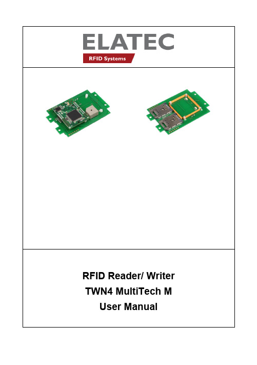
1. IntroductionThe transponder reader module TWN4 MultiTech M is a device for reading and writing RFID transponders. There are different versions of TWN4 devices available, which cover a large range of transponder types both in the frequency range of 125kHz and 13.56MHz.2. Getting Started2.1 Cable ConnectionIn order to start operating a TWN4 transponder reader, it simply has to be connected to a host.2.2 EnumerationOnce the device has been powered up, it is waiting for completion of the enumeration by the USB host. As long as the device is not enumerated, it is entering a minimum power consumption mode, where both LEDs are turned off.2.3 InitializationAfter powering up and enumeration, the device is turning on the built-in transponder reader logic. The green LED is turned on permanently. Some transponder readers need some kind of initialization, which is performed inthis step. After successful initialization, the device sounds a short sequence, which consists of a lower tone followed by a higher tone.2.4 Normal OperationAs soon as the device has completed the initialization, it is entering normal operation. During normal operation the device is searching for a transponder continuously.Detection of a TransponderIf a transponder is detected by the reader, following actions are performed ∙Send the ID to the host. By default, the USB device sends by emulating keystrokes of a keyboard.∙Sound a beep∙Turn off the green LED∙Blink the red LED for two seconds∙Turn on the green LEDWithin the two seconds timeout, where the red LED is blinking, the transponder, which just has been recognized will not be accepted again. This prevents the reader from sending identical IDs more than one time to the host.If during the two seconds timeout of the red LED a different transponder is detected, the complete sequence restarts immediately.Suspend ModeThe transponder reader supports the USB suspend mode. If the USB host is signaling suspend via the USB bus, the transponder reader is turning off most of its power consuming peripherals. During this operation mode, no detection of transponders is possible and all LEDs are turned off.Once the host is resuming to normal operation mode, this is also signaled via the USB bus. Therefore, the transponder reader will resume to normal operation, too.3. List of Antennas HF antennaLF antenna4. Compliance statementsFCC(RF module)Compliance statement:This device complies with Part 15 of the FCC Rules. Operation is subject to the following two conditions: (1) this device may not cause harmful interference, and (2) this device must accept any interference received, including interference that may cause undesired operation.Modification of equipment:The instruction manual of the host shall include the following statement: Changes or modifications made to this equipment not expressly approved by the party responsible for compliance may void the FCC authorization to operate this equipment.Information to the user:(The instruction manual of the host shall include the following statement) A compliance statement as applicable, e.g., for devices subject to part 15 of CFR 47 as specified in §15.19(a)(3), that the product complies with the rules; and the identification, by name, address and telephone number or Internet contact information, of the responsible party, as defined in §2.909. The responsible party for Supplier’s Declaration of Conformity must be located within the United States.Host devicesFCC notes for a host subject to verification or SDoC:For a host device assembled with the certified module and subject to 47 CFR Part 15 verification of class A digital devices, the following statements have to be included in the user manual and the host device has to be labelled as noted below. If the host device is subject to other authorization procedures or parts the appropriate requirements of these authorization procedures or parts apply.Important note:OEM integrator is still responsible for the FCC compliance requirements of the end product, which integrates this module. Appropriate measurements (e.g. 15B compliance) and if applicable additional equipment authorization of the host device to be addressed by the integrator/ manufacturerThe end device must be labeled with:Contains FCC ID: WP5TWN4F17Contains IC: 7948A-TWN4F17HVIN: EL20208Example for SDoC:The compliance information statement shall be included in the user's manual or as a separate sheet. In cases where the manual is provided only in a form other than paper, such as on a computer disk or over the Internet, the information required by this section may be included in the manual in that alternative form, provided the user can reasonably be expected to have the capability to access information in that form. The information may be provided electronically as permitted in §2.935.NOTE: The Commission does not have a required SDoC format. This is an example only and is provided to illustrate the type of information that may be supplied with the product at the time of marketing or importation for meeting the FCC SDoC requirement.For class B devices:FCC §15.105 (b):Note: This equipment has been tested and found to comply with the limits for a Class B digital device, pursuant to part 15 of the FCC Rules. These limits are designed to provide reasonable protection against harmful interference in a residential installation. This equipment generates, uses and can radiate radio frequency energy and, if not installed and used in accordance with the instructions, may cause harmful interference to radio communications. However, there is no guarantee that interference will not occur in a particular installation. If this equipment does cause harmful interference to radio or television reception, which can be determined by turning the equipment off and on, the user is encouraged to try to correct the interference by one or more of the following measures:- Reorient or relocate the receiving antenna.- Increase the separation between the equipment and receiver.- Connect the equipment into an outlet on a circuit different from that to which the Receiver is connected.- Consult the dealer or an experienced radio/TV technician for help.For class A devices:FCC §15.105 (b):NOTE: This equipment has been tested and found to comply with the limits for a Class A digital device, pursuant to part 15 of the FCC Rules. These limits are designed to provide reasonable protection against harmful interference when the equipment is operated in a commercial environment. This equipment generates, uses, and can radiate radio frequency energy and, if not installed and used in accordance with the instruction manual, may cause harmful interference to radio communications. Operation of this equipment in a residential area is likely to cause harmful interference in which case the user will be required to correct the interference at his own expense.CANADA:This device complies with Industry Canada’s license-exempt RSSs. Operation is subject to the following two conditions:(1) This device may not cause interference; and(2) This device must accept any interference, including interference that may cause undesired operation of the device.Le présent appareil est conforme aux CNR d’Industrie Canada applicables aux appareils radio exempts de l icence. L’exploitation est autorisée aux deux conditions suivantes:1) l’appareil ne doit pas produire de brouillage;2) l’utilisateur de l’appareil doit accepter tout brouillage radioélectrique subi, même si le brouillage est susceptible d’en compr omettre le fonctionnement. Special accessories:Where special accessories such as shielded cables and/or special connectors are required to comply with the emission limits, the instruction manual shall include appropriate instructions on the first page of the text describing the installation of the device.Simultaneous transmission:When the host product supports simultaneous-transmission operations the host manufacturer needs to check if there are additional RF exposure filing requirements due to the simultaneous transmissions. When additionalapplication filing for RF exposure compliance demonstration is not required (e. g. the RF module in combination with all simultaneously operating transmitters complies with the RFexposure simultaneous transmission SAR test exclusion requirements), the host manufacturer may do his own evaluation without any filing, using reasonable engineering judgment and testing for confirming compliance with out-of-band, restricted band, and spurious emission requirements in the simultaneous-transmission operating modes. If additional filing is required please contact the person at ELATEC GmbH responsible for certification of the RF module.5. Service AddressIn case of any technical questions, please contact: Elatec GmbHZeppelinstr. 182178 PuchheimGermanyPhone: +49 (0) 89 5529961 0Fax: +49 (0) 89 5529961 29Email: ********************6. TrademarksAll referenced brands, product names, service names and trademarks mentioned in this document are the property of their respective owners.。
kld产品规格书
光盘
■DVD■DVD-R■DVD-RW■VCD■SVCD■CD■CD-R
■CD-RW■MP3□CD-ID□RM□RMVB■DIVX■AVI□其它
视频制式:□PAL□NTSC■PAL/NTEC□其它
外接牒盒:□DVD□VCD□CD(□6碟□10碟□12碟)
TFT屏
ห้องสมุดไป่ตู้类型: □模拟 ■数字
生产厂家: □群创 □AU □CPT □天马 □元太 ■其它
TFT屏尺寸: ■8" □6.5" □6.2" □4.5" □4.2" □3" □2.5"
导航
GPS: ■内置 □外挂
电视
TV: □模拟 □数字 □内置 □外挂 □其它
蓝牙
BLUETOOTH: ■内置 □外挂
蓝牙咪头: ■内置 □外置
二、产品特性
序号
客户要求
范围
备注
1
收星颗数
≥5颗
2
静态电流
≤10MA
三、工作条件
序号
工作条件
范围
备注
1
工作温度范围
-20℃-+60℃
2
工作湿度范围
30%-80%
3
工作电压范围
9V-15.5V
制表:审核:批准:
2.VIDEO:■1CH□CH (□RCA座■RCA线)
3.倒车视频输入 ■有 □无
等响度控制(LOUDNESS):■有□无
其它功能
遥控方式:■红外□RF□有线□无 □其它
出线方式:□散线□ISO线 □小16位输出线 ■其它:专用
时钟:□12小时□24小时■12/24小时
DR5001资料

Electrical Characteristics, 2.4 kbps On-Off KeyedCharacteristicSym NotesMinimum Typical Maximum Units Operating Frequency f O868.15868.55MHzModulation Type OOK Data Rate2.419.2kbpsReceiver Performance (OOK @ 2.4 kbps)Input Current, 3 Vdc Supply I R1.8mA Input Signal for 10-4 BER, 25 C -100dBm Rejection, ±30 MHzR REJ 55dB Sleep to Receive Switch Time(100 ms sleep, -85 dBm signal)t SR 3200µs Sleep Mode CurrentI S 5µA Power Supply Voltage Range V CC 2.7 3.5Vdc Operating Ambient TemperatureT A-20+65°C•Designed for Short-Range Wireless Data Communications •Supports up to 19.2 kbps Encoded Data Transmissions • 3 V, Low Current Operation plus Sleep Mode •Ready to Use OEM ModuleThe DR5001 receiver module is ideal for short-range wireless data applications where robust operation,small size and low power consumption are required. The DR5001 utilizes RFM’s RX6001 amplifier-sequenced hybrid (ASH) architecture to achieve this unique blend of characteristics. The receiver RX6001 is sensitive and stable. A wide dynamic range log detector provides robust performance in the presence of on-channel interference or noise. Two stages of SAW filtering provide excellent receiver out-of -band rejection.The DR5001 includes the RX6001 plus all configuration components in a ready-to-use PCB assembly excel-lent for prototyping and intermediate volume production runs.Absolute Maximum RatingsRatingValueUnitsPower Supply and All Input/Output Pins -0.3 to +4.0V Non-Operating Case Temperature -50 to +100°C Soldering Temperature (10 seconds)230°C868.35 MHz Receiver ModuleDR5001Pin DesciptionsPin Name Description1AGC/VCC This pin is connected directly to the receiver AGCCAP pin. To disable AGC operation, this pin is tied to VCC. To enable AGC operation, a capacitor is placed between this pin and ground. This pin controls the AGC reset operation. A capacitor between this pin and ground sets the minimum time the AGC will hold-in once it is engaged. The hold-in time is set to avoid AGC chat-tering. For a given hold-in time t AGH, the capacitor value C AGC is:C AGC = 19.1* t AGH, where t AGH is in µs and C AGC is in pFA ±10% ceramic capacitor should be used at this pin. The value of C AGC given above provides a hold-in time between t AGH and 2.65* t AGH, depending on operating voltage, temperature, etc. The hold-in time is chosen to allow the AGC to ride through the longest run of zero bits that can occur in a received data stream. The AGC hold-in time can be greater than the peak detector decay time, as discussed below. However, the AGC hold-in time should not be set too long, or the receiver will be slow in returning to full sensitivity once the AGC is engaged by noise or interference. The use of AGC is optional when using OOK modulation with data pulses of at least 30 µs. Active or latched AGC operation is required for ASK modulation and/or for data pulses of less than 30 µs. The AGC can be latched ON once engaged by connecting a 150 K resistor between this pin and ground, instead of a capacitor. AGC operation depends on a functioning peak detector, as discussed below. The AGC capacitor is discharged in the receiver power-down (sleep) mode. Note that provisions are made on the cir-cuit board to install a jumper between this pin and the junction of C2 and L3. Installing the jumper allows either this pin or Pin9 to be used for the Vcc supply when AGC operation is not required.2PK DET This pin is connected directly to the receiver PKDET pin. This pin controls the peak detector operation. A capacitor between this pin and ground sets the peak detector attack and decay times, which have a fixed 1:1000 ratio. For most applications, the attack time constant should be set to 6.4 ms with a 0.027 µF capacitor to ground. (This matches the peak detector decay time constant to the time constant of the 0.1 µF coupling capacitor C3.) A ±10% ceramic capacitor should be used at this pin. The peak detector is used to drive the "dB-below-peak" data slicer and the AGC release function. The AGC hold-in time can be extended beyond the peak detector decay time with the AGC capacitor, as discussed above. Where low data rates and OOK modulation are used, the "dB-below-peak" data slicer and the AGC are optional. In this case, the PKDET pin can be left unconnected, and the AGC pin can be connected to VCC to reduce the number of external components needed. The peak detector capacitor is discharged in the receiver power-down (sleep) mode. See the description of Pin 3 below for further information.3RX BBO This pin is connected directly to the receiver BBOUT pin. On the circuit board, BBOUT also drives the receiver CMPIN pin through C3, a 0.1 µF coupling capacitor (t BBC = 6.4 ms). RX BBO can also be used to drive an external data recovery pro-cess (DSP, etc.). The nominal output impedance of this pin is 1 K. The RX BBO signal changes about 10 mV/dB, with a peak-to-peak signal level of up to 675 mV. The signal at RX BBO is riding on a 1.1 Vdc value that varies somewhat with sup-ply voltage and temperature, so it should be coupled through a capacitor to an external load. A load impedance of 50 K to 500 K in parallel with no more than 10 pF is recommended. Note the AGC reset function is driven by the signal applied to CMPIN through C3. When the receiver is in power-down (sleep) the output impedance of this pin becomes very high, pre-serving the charge on the coupling capacitor(s). The value of C3 on the circuit board has been chosen to match typical data encoding schemes at 2.4 kbps. If C3 is modified to support higher data rates and/or different data encoding schemes and PK DET is being used, make the value of the peak detector capacitor about 1/3 the value of C3.4RX DATA RX DATA is connected directly to the receiver data output pin, RXDATA. This pin will drive a 10 pF, 500 K parallel load. The peak current available from this pin increases with the receiver low-pass filter cutoff frequency. In the power-down (sleep) or receive mode, this pin becomes high impedance. If required, a 1000 K pull-up or pull-down resistor can be used to establish a definite logic state when this pin is high impedance (do not connect the pull-up resistor to a supply voltage higher than 3.5 Vdc or the receiver will be damaged). This pin must be buffered to successfully drive low-impedance loads.5NC 6, 7GND8LPF ADJ This pin is the receiver low-pass filter bandwidth adjust, and is connected directly to the receiver LPFADJ pin. R6 on the cir-cuit board (330 K) is connected between LPFADJ and ground will be in parallel with any external resistor connected to LPF ADJ. The filter bandwidth is set by the parallel resistance of R6 and the external resistor (if used). The equivalent resistor value can range from 330 K to 820 ohms, providing a filter 3 dB bandwidth f LPF from 4.4 kHz to 1.8 MHz. The 3 dB filter bandwidth is determined by:f LPF = 1445/ (330*R LPF/(330 + R LPF)), where R LPF is in kilohms, and f LPF is in kHzA ±5% resistor should be used to set the filter bandwidth. This will provide a 3 dB filter bandwidth between f LPF and 1.3* f LPF with variations in supply voltage, temperature, etc. The filter provides a three-pole, 0.05 degree equiripple phase response. The peak drive current available from RXDATA increases in proportion to the filter bandwidth setting. As shipped, the receiver module is set up for nominal 2.4 kbps operation. An external resistor can be added between Pin 8 and ground to support higher data rates. Preamble training times will not be decreased, however, unless C3 is replaced with a smaller capacitor value (see the descriptions of Pins 2 and 3 above). Refer to sections 1.4.3, 2.5.1 and 2.6.1 in the ASH Transceiver Designer's Guide for additional information on data rate adjustments.9VCC This is the positive supply voltage pin for the module. The operating voltage range is 2.7 to 3.5 Vdc. It is also possible to use Pin 1 as the Vcc input. Please refer to the Pin 1 description above.10GND This is the supply voltage return pin.11CTR1CTR1 is connected to the CNTRL1 control pin on the receiver. CTR1 and CTR0 select the transceiver operating modes. CTR1 and CTR0 both high place the unit in the receive mode. CTR1 and CTR0 both low place the unit in the power-down (sleep) mode. CTR1 is a high-impedance input (CMOS compatible). This pin must be held at a logic level; it cannot be left unconnected. At turn on, the voltage on this pin and CTR0 should rise with VCC until VCC reaches 2.7 Vdc (receive mode). Thereafter, any mode can be selected.12CTR0CTR0 is connected to the CNTRL0 control pin on the receiver CTR0 is used with CTR1 to control the operating modes of the receiver. CTR0 is a high-impedance input (CMOS compatible). This pin must be held at a logic level; it cannot be left uncon-nected. At turn on, the voltage on this pin and CTR1 should rise with VCC until VCC reaches 2.7 Vdc (receive mode). There-after, any mode can be selected.13RFIO RFIO is the RF input/output pin. A matching circuit for a 50 ohm load (antenna) is implemented on the circuit board between this pin and the receiver SAW filter transducer.14RF GND This pin is the RF ground (return) to be used in conjunction with the RFIO pin. For example, when connecting the transceiver module to an external antenna, the coaxial cable ground is connected this pin and the coaxial cable center conductor is con-nected to RFIO.Note: Preliminary specifications, subject to change without notice.。
DMN2004DWK-7;中文规格书,Datasheet资料
Features• Dual N-Channel MOSFET • Low On-Resistance • Low Gate Threshold Voltage • Low Input Capacitance • Fast Switching Speed • Low Input/Output Leakage • Ultra-Small Surface Mount Package • Lead Free By Design/RoHS Compliant (Note 1) • ESD Protected up to 2KV • "Green" Device (Note 2) • Qualified to AEC-Q101 standards for High ReliabilityMechanical Data• Case: SOT363 • Case Material: Molded Plastic, “Green” MoldingCompound. UL Flammability Classification Rating 94V-0 • Moisture Sensitivity: Level 1 per J-STD-020 • Terminal Connections: See Diagram • Terminals: Finish - Matte Tin annealed over Alloy 42leadframe. Solderable per MIL-STD-202, Method 208 • Weight: 0.006 grams (approximate)Ordering Information (Note 3)Part Number Case Packaging DMN2004DWK-7SOT363 3000/Tape & ReelNotes: 1. No purposefully added lead.2. Diodes Inc.’s “Green” policy can be found on our website at .3. For packaging details, go to our website at .Marking InformationDate Code KeyYear 2006 2007 2008 2009 2010 2011 2012 2013 2014 2015 2016 2017 Code T U V W X Y Z A B C D EMonth Jan Feb Mar Apr MayJun Jul Aug Sep Oct Nov Dec Code 1 2 3 4 5 6 7 8 9 O NDSOT363Top ViewTop ViewInternal SchematicNAB = Marking Code YM = Date Code Marking Y = Year (ex: T = 2006) M = Month (ex: 9 = September) ESD PROTECTED TO 2kVNAB YM N A B Y MMaximum Ratings @T A = 25°C unless otherwise specifiedCharacteristic Symbol Value UnitsDrain-Source Voltage V DSS20 V Gate-Source VoltageV GSS±8 V Drain Current (Note 4)SteadyStateT A = 25°C T A = 85°CI D 540 390mAPulsed Drain Current (Note 5) I DM1.5 AThermal Characteristics @T A = 25°C unless otherwise specifiedCharacteristic Symbol Value UnitsTotal Power Dissipation (Note 4) P D 200 mW Thermal Resistance, Junction to Ambient R θJA 625 °C/W Operating and Storage Temperature Range T J, T STG -65 to +150 °CElectrical Characteristics @T A = 25°C unless otherwise specifiedCharacteristic Symbol Min Typ Max Unit Test ConditionOFF CHARACTERISTICS (Note 6) Drain-Source Breakdown Voltage BV DSS 20 ⎯ ⎯ V V GS = 0V, I D = 10μA Zero Gate Voltage Drain Current I DSS ⎯ ⎯ 1 μA V DS = 16V, V GS= 0V Gate-Source Leakage I GSS ⎯ ⎯ ±1 μA V GS = ±4.5V, V DS = 0V ON CHARACTERISTICS (Note 6)Gate Threshold Voltage V GS(th)0.5 ⎯ 1.0 V V DS = V GS , I D = 250μA Static Drain-Source On-Resistance R DS (ON)⎯ 0.4 0.5 0.7 0.550.70 0.9 Ω V GS = 4.5V, I D = 540mA VGS = 2.5V, I D = 500mA V GS = 1.8V, I D = 350mAForward Transfer Admittance |Y fs |200 ⎯ ⎯ ms V DS =10V, I D = 0.2A Diode Forward Voltage (Note 6) V SD0.5 ⎯ 1.4 V V GS = 0V, I S = 115mA DYNAMIC CHARACTERISTICSInput Capacitance C iss⎯ ⎯ 150 pF V DS = 16V, V GS = 0Vf = 1.0MHzOutput Capacitance C oss⎯ ⎯ 25 pF Reverse Transfer Capacitance C rss⎯ ⎯ 20 pF Notes:4. Device mounted on FR-4 PCB.5. Pulse width ≤10μS, Duty Cycle ≤1%.6. Short duration pulse test used to minimize self-heating effect.V , DRAIN-SOURCE VOLTAGE (V)Fig. 1 Typical Output CharacteristicsDS I , D R A I N C U R R E N T (A )D V , GATE-SOURCE VOLTAGE (V)Fig. 2 GS Reverse Drain Current vs. Source-Drain VoltageT , CHANNEL TEMPERATURE (°C)Fig. 3 Gate Threshold Voltage vs. Channel Temperaturech 0.1I DRAIN CURRENT (A)Fig. 4 Static Drain-Source On-Resistance Vs. Drain Current D ,1R , S T A T I C D R A I N -S O U R C E O N -R E S I S T A N C E ()D S (o n )ΩI , DRAIN CURRENT (A)Fig. 5 Static Drain-Source On-Resistance vs. Drain CurrentD R , S T A T I C D R A I N -S O U R CE O N -R E S I S T A N C E ()D S (o n )ΩI , DRAIN CURRENT (A)Fig. 7DOn-Resistance vs. Drain Current and Gate Voltage T , JUNCTION TEMPERATURE (C)Fig. 8 j °Static Drain-Source, On-Resistance vs. TemperatureI , D R A I N -S O U R C E L E A K A G E C U R R E N T (n A )D SS I , R E V E R S E D R A I N C U R R E N T (A )DR 1000I , DRAIN CURRENT (mA)DFig. 11 Forward Transfer Admittance vs. Drain Current|Y |, F O R W A R D T R A N S F E R A D M I T T A N C E(S )fs V , DRAIN SOURCE VOLTAGE (V)DS Fig. 12 Capacitance VariationPackage Outline DimensionsSOT363Dim Min Max A 0.10 0.30 B 1.15 1.35 C 2.00 2.20 D 0.65 Typ F 0.40 0.45 H 1.80 2.20 J 0 0.10 K 0.901.00 L 0.25 0.40 M 0.10 0.22α0° 8° All Dimensions in mmSuggested Pad LayoutIMPORTANT NOTICEDIODES INCORPORATED MAKES NO WARRANTY OF ANY KIND, EXPRESS OR IMPLIED, WITH REGARDS TO THIS DOCUMENT, INCLUDING, BUT NOT LIMITED TO, THE IMPLIED WARRANTIES OF MERCHANTABILITY AND FITNESS FOR A PARTICULAR PURPOSE (AND THEIR EQUIVALENTS UNDER THE LAWS OF ANY JURISDICTION).Diodes Incorporated and its subsidiaries reserve the right to make modifications, enhancements, improvements, corrections or other changes without further notice to this document and any product described herein. Diodes Incorporated does not assume any liability arising out of the application or use of this document or any product described herein; neither does Diodes Incorporated convey any license under its patent or trademark rights, nor the rights of others. Any Customer or user of this document or products described herein in such applications shall assume all risks of such use and will agree to hold Diodes Incorporated and all the companies whose products are represented on Diodes Incorporated website, harmless against all damages.Diodes Incorporated does not warrant or accept any liability whatsoever in respect of any products purchased through unauthorized sales channel. Should Customers purchase or use Diodes Incorporated products for any unintended or unauthorized application, Customers shall indemnify and hold Diodes Incorporated and its representatives harmless against all claims, damages, expenses, and attorney fees arising out of, directly or indirectly, any claim of personal injury or death associated with such unintended or unauthorized application.Products described herein may be covered by one or more United States, international or foreign patents pending. Product names and markings noted herein may also be covered by one or more United States, international or foreign trademarks.LIFE SUPPORTDiodes Incorporated products are specifically not authorized for use as critical components in life support devices or systems without the express written approval of the Chief Executive Officer of Diodes Incorporated. As used herein:A. Life support devices or systems are devices or systems which: 1. are intended to implant into the body, or2. support or sustain life and whose failure to perform when properly used in accordance with instructions for use provided in thelabeling can be reasonably expected to result in significant injury to the user.B. A critical component is any component in a life support device or system whose failure to perform can be reasonably expected to cause the failure of the life support device or to affect its safety or effectiveness.Customers represent that they have all necessary expertise in the safety and regulatory ramifications of their life support devices or systems, and acknowledge and agree that they are solely responsible for all legal, regulatory and safety-related requirements concerning their products and any use of Diodes Incorporated products in such safety-critical, life support devices or systems, notwithstanding any devices- or systems-related information or support that may be provided by Diodes Incorporated. Further, Customers must fully indemnify Diodes Incorporated and its representatives against any damages arising out of the use of Diodes Incorporated products in such safety-critical, life support devices or systems.Copyright © 2011, Diodes IncorporatedDimensions Value (in mm)Z 2.5 G 1.3 X 0.42 Y 0.6 C1 1.9 C2 0.65XZYC1C2C2G分销商库存信息: DIODESDMN2004DWK-7。
NI cDAQ

SPECIFICA TIONSNI cDAQ™-91811-Slot, Ethernet CompactDAQ ChassisDefinitionsWarranted specifications describe the performance of a model under stated operating conditions and are covered by the model warranty.Characteristics describe values that are relevant to the use of the model under stated operating conditions but are not covered by the model warranty.•Typical specifications describe the expected performance met by a majority of the models.•Nominal specifications describe parameters and attributes that may be useful in operation. Specifications are Typical unless otherwise noted.ConditionsSpecifications are valid at 25 °C unless otherwise noted.Analog InputInput FIFO size127 samplesMaximum sample rate1Determined by the C Series moduleTiming accuracy250 ppm of sample rateTiming resolution212.5 nsNumber of channels supported Determined by the C Series module 1Performance dependent on type of installed C Series module and number of channels in the task.2Does not include group delay. For more information, refer to the documentation for each C Series module.Analog OutputNumber of channels supportedHardware-timed taskOnboard regeneration16Non-regeneration Determined by the C Series module Non-hardware-timed task Determined by the C Series module Maximum update rateOnboard regeneration 1.6 MS/s (multi-channel, aggregate)Non-regeneration Determined by the C Series module Timing accuracy50 ppm of sample rateTiming resolution12.5 nsOutput FIFO sizeOnboard regeneration8,191 samples shared among channels used Non-regeneration127 samplesAO waveform modes Non-periodic waveform,periodic waveform regeneration mode fromonboard memory,periodic waveform regeneration from hostbuffer including dynamic updateDigital Waveform CharacteristicsWaveform acquisition (DI) FIFOParallel modules511 samplesSerial modules63 samplesWaveform generation (DO) FIFOParallel modules2,047 samplesSerial modules63 samplesDigital input sample clock frequencyStreaming to application memory System-dependentFinite0 MHz to 10 MHz2| | NI cDAQ-9181 SpecificationsDigital output sample clock frequencyStreaming from application memory System-dependentRegeneration from FIFO0 MHz to 10 MHzFinite0 MHz to 10 MHzTiming accuracy50 ppmGeneral-Purpose Counters/TimersNumber of counters/timers4Resolution32 bitsCounter measurements Edge counting, pulse, semi-period, period,two-edge separation, pulse widthPosition measurements X1, X2, X4 quadrature encoding withChannel Z reloading; two-pulse encoding Output applications Pulse, pulse train with dynamic updates,frequency division, equivalent time sampling Internal base clocks80 MHz, 20 MHz, 100 kHzExternal base clock frequency0 MHz to 20 MHzBase clock accuracy50 ppmOutput frequency0 MHz to 20 MHzInputs Gate, Source, HW_Arm, Aux, A, B, Z,Up_DownRouting options for inputs Any module PFI, analog trigger, many internalsignalsFIFO Dedicated 127-sample FIFOFrequency GeneratorNumber of channels1Base clocks20 MHz, 10 MHz, 100 kHzDivisors 1 to 16 (integers)Base clock accuracy50 ppmOutput Any module PFI terminalNI cDAQ-9181 Specifications| © National Instruments| 3Module PFI CharacteristicsFunctionality Static digital input, static digital output, timinginput, and timing outputTiming output sources3Many analog input, analog output, counter,digital input, and digital output timing signals Timing input frequency0 MHz to 20 MHzTiming output frequency0 MHz to 20 MHzDigital TriggersSource Any module PFI terminalPolarity Software-selectable for most signalsAnalog input function Start Trigger, Reference Trigger,Pause Trigger, Sample Clock,Sample Clock TimebaseAnalog output function Start Trigger, Pause Trigger, Sample Clock,Sample Clock TimebaseCounter/timer function Gate, Source, HW_Arm, Aux, A, B, Z,Up_DownModule I/O StatesAt power-on Module-dependent. Refer to the documentationfor each C Series module.Network InterfaceNetwork protocols TCP/IP, UDPNetwork ports used HTTP:80 (configuration only), TCP:3580;UDP:5353 (configuration only), TCP:5353(configuration only); TCP:31415; UDP:7865(configuration only), UDP:8473 (configurationonly)Network IP configuration DHCP + Link-Local, DHCP, Static,Link-Local3Actual available signals are dependent on type of installed C Series module.4| | NI cDAQ-9181 SpecificationsHigh-performance data streams6Data stream types available Analog input, analog output, digital input,digital output, counter/timer input,counter/timer output, NI-XNET4Default MTU size1500 bytesEthernetNetwork interface100 Base-TX, full-duplex; 100 Base-TX,half-duplex; 10 Base-T, full-duplex; 10 Base-T,half-duplexCommunication rates10/100 Mbps, auto-negotiatedMaximum cabling distance100 m/segmentPower RequirementsCaution The protection provided by the NI cDAQ-9181 chassis can be impaired ifit is used in a manner not described in the NI cDAQ-9181/9184/9188/9191 UserManual.Note Some C Series modules have additional power requirements. For moreinformation about C Series module power requirements, refer to the documentationfor each C Series module.Note Sleep mode for C Series modules is not supported in the NI cDAQ-9181.V oltage input range9 V to 30 VMaximum power consumption5 5 W4When a session is active, CAN or LIN (NI-XNET) C Series modules use a total of two data streams regardless of the number of NI-XNET modules in the chassis.5Includes maximum 1 W module load per slot across rated temperature and product variations.NI cDAQ-9181 Specifications| © National Instruments| 5Note The maximum power consumption specification is based on a fully populatedsystem running a high-stress application at elevated ambient temperature and withall C Series modules consuming the maximum allowed power.Power input connector 2 positions 3.5 mm pitch mini-combicon screwterminal with screw flanges, Phoenix Contact1727566Power input mating connector Sauro CTF020V8, Phoenix Contact 1714977,or equivalentPhysical CharacteristicsWeight (unloaded)Approx. 470 g (16.6 oz)Dimensions (unloaded)194.0 mm × 88.7 mm × 33.6 mm(7.64 in. × 3.49 in. × 1.32 in.) Refer to thefollowing figure.Screw-terminal wiringGauge0.5 mm 2 to 2.1 mm2 (20 AWG to 14 AWG)copper conductor wireWire strip length 6 mm (0.24 in.) of insulation stripped from theendTemperature rating85 °CTorque for screw terminals0.20 N · m to 0.25 N · m (1.8 lb · in. to2.2 lb · in.)Wires per screw terminal One wire per screw terminalConnector securementSecurement type Screw flanges providedTorque for screw flanges0.20 N · m to 0.25 N · m (1.8 lb · in. to2.2 lb · in.)If you need to clean the chassis, wipe it with a dry towel.6| | NI cDAQ-9181 SpecificationsFigure 1. NI cDAQ-9181 DimensionsSafety VoltagesConnect only voltages that are within these limits.V terminal to C terminal30 V maximum, Measurement Category IMeasurement Category I is for measurements performed on circuits not directly connected to the electrical distribution system referred to as MAINS voltage. MAINS is a hazardous live electrical supply system that powers equipment. This category is for measurements of voltages from specially protected secondary circuits. Such voltage measurements include signal levels,special equipment, limited-energy parts of equipment, circuits powered by regulated low-voltage sources, and electronics.Caution Do not connect the system to signals or use for measurements withinMeasurement Categories II, III, or IV .NI cDAQ-9181 Specifications | © National Instruments | 7Note Measurement Categories CAT I and CAT O (Other) are equivalent. These testand measurement circuits are not intended for direct connection to the MAINsbuilding installations of Measurement Categories CAT II, CAT III, or CAT IV.Environmental0 °C to 55 °COperating temperature (IEC 60068-2-1and IEC 60068-2-2)Caution To maintain product performance and accuracy specifications when theambient temperature is between 45 and 55 °C, you must mount the chassishorizontally to a metal panel or surface using the screw holes or the panel mount kit.Measure the ambient temperature at each side of the CompactDAQ system 63.5 mm(2.5 in.) from the side and 25.4 mm (1.0 in.) from the rear cover of the system. Forfurther information about mounting configurations, go to /info and enterthe Info Code cdaqmounting.Storage temperature (IEC 60068-2-1 and-10 °C to 70 °CIEC 60068-2-2)Ingress protection IP 30Operating humidity (IEC 60068-2-56)10% to 90% RH, noncondensingStorage humidity (IEC 60068-2-56)5% to 95% RH, noncondensingPollution Degree (IEC 60664)2Maximum altitude5,000 mIndoor use only.Hazardous LocationsU.S. (UL)Class I, Division 2, Groups A, B, C, D, T4;Class I, Zone 2, AEx nA IIC T4Canada (C-UL)Class I, Division 2, Groups A, B, C, D, T4;Class I, Zone 2, Ex nA IIC T4Europe (ATEX) and International (IECEx)Ex nA IIC T4 Gc8| | NI cDAQ-9181 SpecificationsShock and VibrationTo meet these specifications, you must direct mount the NI cDAQ-9181 system and affix ferrules to the ends of the terminal lines.Operational shock30 g peak, half-sine, 11 ms pulse (Tested inaccordance with IEC 60068-2-27. Test profiledeveloped in accordance withMIL-PRF-28800F.)Random vibrationOperating 5 Hz to 500 Hz, 0.3 g rmsNon-operating 5 Hz to 500 Hz, 2.4 g rms (Tested in accordancewith IEC 60068-2-64. Non-operating testprofile exceeds the requirements ofMIL PRF-28800F, Class 3.)Safety and Hazardous Locations StandardsThis product is designed to meet the requirements of the following electrical equipment safety standards for measurement, control, and laboratory use:•IEC 61010-1, EN 61010-1•UL 61010-1, CSA C22.2 No. 61010-1•EN 60079-0:2012, EN 60079-15:2010•IEC 60079-0: Ed 6, IEC 60079-15; Ed 4•UL 60079-0; Ed 6, UL 60079-15; Ed 4•CSA 60079-0:2011, CSA 60079-15:2012Note For UL and other safety certifications, refer to the product label or the OnlineProduct Certification section.Electromagnetic CompatibilityThis product meets the requirements of the following EMC standards for electrical equipment for measurement, control, and laboratory use:•EN 61326-1 (IEC 61326-1): Class A emissions; Basic immunity•EN 55011 (CISPR 11): Group 1, Class A emissions•EN 55022 (CISPR 22): Class A emissions•EN 55024 (CISPR 24): Immunity•AS/NZS CISPR 11: Group 1, Class A emissions•AS/NZS CISPR 22: Class A emissionsNI cDAQ-9181 Specifications| © National Instruments| 9•FCC 47 CFR Part 15B: Class A emissions•ICES-001: Class A emissionsNote In the United States (per FCC 47 CFR), Class A equipment is intended foruse in commercial, light-industrial, and heavy-industrial locations. In Europe,Canada, Australia and New Zealand (per CISPR 11) Class A equipment is intendedfor use only in heavy-industrial locations.Note Group 1 equipment (per CISPR 11) is any industrial, scientific, or medicalequipment that does not intentionally generate radio frequency energy for thetreatment of material or inspection/analysis purposes.Note For EMC declarations and certifications, and additional information, refer tothe Online Product Certification section.CE ComplianceThis product meets the essential requirements of applicable European Directives, as follows:•2014/35/EU; Low-V oltage Directive (safety)•2014/30/EU; Electromagnetic Compatibility Directive (EMC)•2014/34/EU; Potentially Explosive Atmospheres (ATEX)Online Product CertificationRefer to the product Declaration of Conformity (DoC) for additional regulatory compliance information. To obtain product certifications and the DoC for this product, visit / certification, search by model number or product line, and click the appropriate link in the Certification column.Environmental ManagementNI is committed to designing and manufacturing products in an environmentally responsible manner. NI recognizes that eliminating certain hazardous substances from our products is beneficial to the environment and to NI customers.For additional environmental information, refer to the Minimize Our Environmental Impact web page at /environment. This page contains the environmental regulations and directives with which NI complies, as well as other environmental information not included in this document.10| | NI cDAQ-9181 SpecificationsWaste Electrical and Electronic Equipment (WEEE) EU Customers At the end of the product life cycle, all NI products must bedisposed of according to local laws and regulations. For more information abouthow to recycle NI products in your region, visit /environment/weee.电子信息产品污染控制管理办法(中国RoHS)中国客户National Instruments符合中国电子信息产品中限制使用某些有害物质指令(RoHS)。
NID5001N资料

NID5001NPreferred DeviceSelf−protected FET with Temperature and Current LimitHDPlus devices are an advanced series of power MOSFETs which utilize ON Semicondutor’s latest MOSFET technology process to achieve the lowest possible on−resistance per silicon area while incorporating smart features. Integrated thermal and current limits work together to provide short circuit protection. The devices feature an integrated Drain−to−Gate Clamp that enables them to withstand high energy in the avalanche mode. The Clamp also provides additional safety margin against unexpected voltage transients.Electrostatic Discharge (ESD) protection is provided by an integrated Gate−to−Source Clamp.Features•Low R DS(on)•Current Limitation•Thermal Shutdown with Automatic Restart •Short Circuit Protection•I DSS Specified at Elevated Temperature •Avalanche Energy Specified•Slew Rate Control for Low Noise Switching •Overvoltage Clamped ProtectionMOSFET MAXIMUM RATINGS (T= 25°C unless otherwise noted)1.Minimum FR4 PCB, steady state.2.Mounted onto a 2″square FR4 board (1″square, 2 oz. Cu 0.06″ thick single−sided, t = steady state).Device Package Shipping †ORDERING INFORMATIONNID5001NT4DPAK2500/T ape & ReelPreferred devices are recommended choices for future use and best overall value.*Max current may be limited below this value depending on input conditions.†For information on tape and reel specifications,including part orientation and tape sizes, please refer to our Tape and Reel Packaging Specification Brochure, BRD8011/D.MOSFET ELECTRICAL CHARACTERISTICS (T = 25°C unless otherwise noted)ESD ELECTRICAL CHARACTERISTICS(T = 25°C unless otherwise noted)2816I D , D R A I N C U R R E N T (A M P S )1240R D S (o n ), D R A I N −T O −S O U R C E R E S I S T A N C E (W )−500−252550100Figure 5. On−Resistance Variation withTemperature T J , JUNCTION TEMPERATURE (°C)75R D S (o n ), D R A I N −T O −S O U R C E R E S I S T A N C E (N O R M A L I Z E D )4525Figure 6. Drain−to−Source Leakage Currentvs. VoltageV DS , DRAIN−TO−SOURCE VOLTAGE (VOLTS)151020840303524200.90.020V SD , SOURCE−TO−DRAIN VOLTAGE (VOLTS)Figure 7. Diode Forward Voltage vs. CurrentI S , S O U R C E C U R R E N T (A M P S )0.140.70.50.30.10.080.12Figure 8. Maximum Rated Forward BiasedSafe Operating AreaV DS , DRAIN−TO−SOURCE VOLTAGE (VOLTS)I D , D R A I N C U R R E N T (A M P S )0.80.60.40.060.04PACKAGE DIMENSIONSDPAKCASE 369C−01ISSUE OV SDIM MIN MAX MIN MAXMILLIMETERSINCHESA0.2350.245 5.97 6.22B0.2500.265 6.35 6.73C0.0860.094 2.19 2.38D0.0270.0350.690.88E0.0180.0230.460.58F0.0370.0450.94 1.14G0.180 BSC 4.58 BSCH0.0340.0400.87 1.01J0.0180.0230.460.58K0.1020.114 2.60 2.89L0.090 BSC 2.29 BSCR0.1800.215 4.57 5.45S0.0250.0400.63 1.01U0.020−−−0.51−−−V0.0350.0500.89 1.27Z0.155−−− 3.93−−−STYLE 2:PIN 1.GATE2.DRAIN3.SOURCE4.DRAINǒmminchesǓSCALE 3:1*For additional information on our Pb−Free strategy and solderingdetails, please download the ON Semiconductor Soldering andMounting Techniques Reference Manual, SOLDERRM/D.SOLDERING FOOTPRINT*ON Semiconductor and are registered trademarks of Semiconductor Components Industries, LLC (SCILLC). SCILLC reserves the right to make changes without further notice to any products herein. SCILLC makes no warranty, representation or guarantee regarding the suitability of its products for any particular purpose, nor does SCILLC assume any liability arising out of the application or use of any product or circuit, and specifically disclaims any and all liability, including without limitation special, consequential or incidental damages.“Typical” parameters which may be provided in SCILLC data sheets and/or specifications can and do vary in different applications and actual performance may vary over time. All operating parameters, including “Typicals” must be validated for each customer application by customer’s technical experts. SCILLC does not convey any license under its patent rights nor the rights of others. SCILLC products are not designed, intended, or authorized for use as components in systems intended for surgical implant into the body, or other applications intended to support or sustain life, or for any other application in which the failure of the SCILLC product could create a situation where personal injury or death may occur. Should Buyer purchase or use SCILLC products for any such unintended or unauthorized application, Buyer shall indemnify and hold SCILLC and its officers, employees, subsidiaries, affiliates, and distributors harmless against all claims, costs, damages, and expenses, and reasonable attorney fees arising out of, directly or indirectly, any claim of personal injury or death associated with such unintended or unauthorized use, even if such claim alleges that SCILLC was negligent regarding the design or manufacture of the part. SCILLC is an Equal Opportunity/Affirmative Action Employer. This literature is subject to all applicable copyright laws and is not for resale in any manner.PUBLICATION ORDERING INFORMATION。
Powerline Nano500 设备说明书
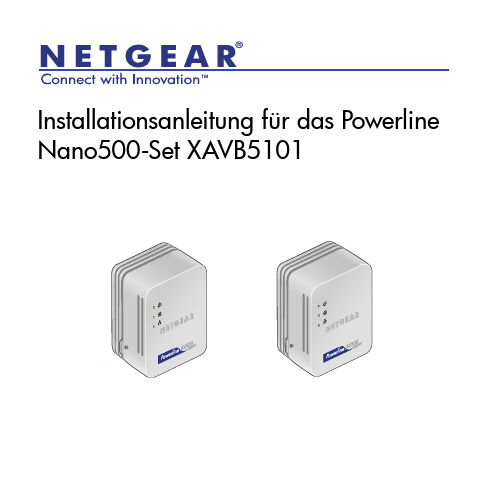
Installationsanleitung für das Powerline© 2012 NETGEAR, Inc. Alle Rechte vorbehalten.Kein Teil dieser Publikation darf ohne schriftliche Genehmigung von NETGEAR, Inc. in irgendeiner Form oder Weise reproduziert, übertragen, transkribiert, in einem Datenabfragesystem gespeichert oder in irgendeine Sprache übersetzt werden.Stapeln Sie elektronische Geräte NICHT, stellen Sie Geräte NICHT in engen Räumen auf, oder legen Sie sie NICHT in Schubladen. Stellen Sie sicher, dass das Gerät in einem freien Abstand von mindestens 5 Zentimetern aufgestellt ist.Technischer SupportDanke, dass Sie sich für NETGEAR entschieden haben. Unter können Sie Ihr Produkt registrieren, die neuesten Produkt-Updates beziehen oder den Online-Support in Anspruch nehmen.Telefon (nur USA und Kanada): 1-888-NETGEARTelefon (andere Länder):Siehe /app/answers/detail/a_id/984.MarkenNETGEAR, das NETGEAR-Logo und Connect with Innovation sind Marken und/oder eingetragene Marken von NETGEAR, Inc. und/oder seiner Tochtergesellschaften in den USA und/oder anderen Ländern. Informationen können ohne vorherige Ankündigung geändert werden. Andere Marken- und Produktnamen sind eingetragene Marken oder Marken der jeweiligen Inhaber. © 2011 NETGEAR, Inc. Alle Rechte vorbehalten. NutzungsbedingungenZur Verbesserung des internen Designs, des Betriebs und/oder der Zuverlässigkeit behält NETGEAR sich das Recht vor, die in diesem Dokument beschriebenen Produkte ohne vorherige Ankündigung zu ändern. NETGEAR lehnt im Zusammenhang mit dem Einsatz oder der Anwendung der hier beschriebenen Produkte oder Schaltpläne jegliche Haftung ab.Hardware-FunktionenPower-LEDPowerline-LEDNetzwerk-LEDSecurity-TasteReset-TasteNetzwerkanschlussBeschreibung der LEDsDie LEDs zeigen den Status der Powerline-Adapter an.• Wenn Sie den Adapter anschließen, leuchtet die Power LED auf und leuchtet grün.Der Adapter ist nicht aktiv, wenn seit mehr als 10 Minuten keine Netzwerkverbindung vorhanden ist. Der Adapter wechselt in den Energiesparmodus, und die Power-LED leuchtet gelb .• Die Powerline-LED leuchtet, wenn der Adapter mindestens ein anderes kompatibles Powerline-Gerät findet.Die Funktion Pick A Plug ermöglicht Ihnen die Auswahl desAnschlusses mit der besten Übertragungsrate, zu erkennen an der Farbe der Powerline-LED:- Grün: Übertragungsrate > 80 MBit/s (am besten)- Gelb: Übertragungsrate > 50 und < 80 MBit/s (besser)- Rot: Übertragungsrate < 50 MBit/s (gut)• Die Netzwerk-LED leuchtet, wenn Sie ein eingeschaltetes Netzwerkgerät mit mindestens einem Netzwerkanschlussverbinden.TastenbeschreibungenDie Tasten an Ihren Powerline-Adaptern haben die folgenden Funktionen:• Reset-Taste — Mit der Reset-Taste kann das Powerline-Gerät auf die werkseitigen Voreinstellungen zurückgesetzt werden.Halten Sie die Reset-Taste für eine Zeitspanne von 1 bis5 Sekunden lang gedrückt, und lassen Sie sie wieder los.• Security-Taste — Die Security-Taste dient zum Festlegen der Sicherheit zwischen den Powerline-Geräten. Halten Sie dieSecurity-Taste für eine Zeitspanne von 2 bis 5 Sekunden lang gedrückt, und lassen Sie sie wieder los.Weitere Informationen zu den Einstellungen für die Sicherheit finden Sie unter Installieren der Powerline-Adapter auf Seite 7.Installieren der Powerline-AdapterAdaptern.Schritt 1:Stecken Sie diezwei Powerline-eine Steckdose.Schritt 2:Drücken Sie aufSecurity-Tastebis 5 Sekundenlang, und lassenSie sie los. DiePowerline-LEDblinkt.Die Power-LEDleuchtet auf. Diestellungen istabgeschlossen.Hinzufügen eines neuen Powerline-Adapters zum sicherenTechnischer SupportVielen Dank, dass Sie sich für Produkte von NETGEAR entschieden haben.Nach der Installation des Geräts können Sie das Produkt mit der Seriennummer, die Sie auf dem Etikett Ihres Produkts finden, unter https:// registrieren.Die Registrierung ist Voraussetzung für die Nutzung des telefonischen Supports. Die Registrierung über die NETGEAR-Website wird dringend empfohlen.Produkt-Updates und Internetsupport finden Sie unter.Weitere Informationen zur Einrichtung, Konfiguration und Verwendung Ihres Powerline-Adapters finden Sie im Benutzerhandbuch.Kompatible NETGEAR Powerline-Geräte Ihr Powerline-Adapter kann ein Powerline-Netzwerk mit diesen kompatiblen NETGEAR-Geräten teilen: XAV101, XAV1004,XAV2001, XAV1101, XAV1301, XAV1401, XAV1601, XAV2101, XAV2501, XAV2602, XAV5001, XAV5501, XAV5601 und XAV5004. Eine vollständige Liste HomePlug-AV-zertifizierter Geräte finden Sie unter /certified_products.VorschrifteneinhaltungKonformitätserklärungenDie vollständige DoC finden Sie auf der NETGEAR-Website mit der EU-Konformitätserklärung unter: /app/answers/detail/a_id/11621/. Informationen über GNU General Public License (GPL) finden Sie unter/app/answers/detail/a_id/2649.WARNUNG: Stapeln Sie elektronische Geräte NICHT, stellen Sie sie NICHT in engenRäumen oder auf Teppichboden auf, und legen Sie sie NICHT in Schubladen. Stellen Sie sicher, dass das Gerät in einem freien Abstand von mindestens 5 Zentimetern aufgestellt ist.Dieses Symbol wurde in Übereinstimmung mit der EU-Richtlinie 2002/96/EGüber Elektro- und Elektronik-Altgeräte (WEEE-Richtlinie) hier angebracht. DieEntsorgung dieses Produkts innerhalb der Europäischen Union sollte inÜbereinstimmung mit den in Ihrem Land zur Implementierung der WEEE-Richtlinie geltenden Gesetzen gehandhabt werden.NETGEAR, das NETGEAR-Logo und Connect with Innovation sind Marken und/oder eingetragene Marken von NETGEAR, Inc. und/oder seiner Tochtergesellschaften in den USA und/oder anderen Ländern. Informationen können ohne vorherige Ankündigunggeändert werden. Andere Marken- und Produktnamen sind Marken oder eingetragene Marken der jeweiligen Inhaber. © 2012 NETGEAR, Inc. Alle Rechte vorbehalten.NETGEAR, Inc.350 East Plumeria Drive San Jose, CA 95134, USAJanuar 2012。
DMN2005LP4K-7;中文规格书,Datasheet资料

N-CHANNEL ENHANCEMENT MODE MOSFETFeatures• Low On-Resistance • Very Low Gate Threshold Voltage, 0.9V Max. • Fast Switching Speed • Low Input/Output Leakage • Ultra-Small Surface Mount Package • Totally Lead-Free & Fully RoHS Compliant (Notes 1 & 2) • Halogen and Antimony Free. “Green” Device (Note 3) • ESD Protected Gate • Ultra Low Profile Package • Qualified to AEC-Q101 Standards for High ReliabilityMechanical Data• Case: X2-DFN1006-3 • Case Material: Molded Plastic, “Green” Molding Compound. ULFlammability Classification Rating 94V-0 • Moisture Sensitivity: Level 1 per J-STD-020 • Terminal Connections: See Diagram • Terminals: Finish ⎯NiPdAu over Copper leadframe. Solderableper MIL-STD-202, Method 208 • Weight: 0.001 gramsOrdering Information (Note 4)Part Number Marking Reel size (inches) Tape width (mm) Quantity per reelDMN2005LP4K-7 DN 7 8 3000 DMN2005LP4K-7B DN 7 8 10,000Notes: 1. No purposely added lead. Fully EU Directive 2002/95/EC (RoHS) & 2011/65/EU (RoHS 2) compliant.2. See for more information about Diodes Incorporated’s definitions of Halogen- and Antimony-free, "Green" and Lead-free.3. Halogen- and Antimony-free "Green” products are defined as those which contain <900ppm bromine, <900ppm chlorine (<1500ppm total Br + Cl) and <1000ppm antimony compounds.4. For packaging details, go to our website at .Marking Informatione4X2-DFN1006-3Bottom ViewEquivalent CircuitTop View Pin-OutBody DiodeDSGESD PROTECTEDDN = Product Type Marking CodeDNDMN2005LP4K-7DMN2005LP4K-7BTop View Bar Denotes Gate and Source SideTop View Dot Denotes Drain SideMaximum Ratings (@T A = 25°C unless otherwise specified.)Characteristic Symbol Value UnitDrain-Source VoltageV DSS20 V Gate-Source VoltageV GSS ±10 V Drain Current per element (Note 5) Continuous Pulsed (Note 6) I D300 350mAThermal CharacteristicsCharacteristic Symbol Value UnitTotal Power Dissipation (Note 5) P D 400 mW Thermal Resistance, Junction to Ambient R θJA 280 °C/WOperating and Storage Temperature Range T J , T STG-65 to +150°CElectrical Characteristics (@T A = 25°C unless otherwise specified.)Characteristic Symbol Min Typ Max Unit Test ConditionOFF CHARACTERISTICS (per element) (Note 7)Drain-Source Breakdown Voltage BV DSS20 ⎯ ⎯ V V GS = 0V, I D = 100µA Zero Gate Voltage Drain Current I DSS ⎯ ⎯ 10 µA V DS = 17V, V GS = 0V Gate-Source LeakageI GSS ⎯ ⎯ ±5µAV GS = ±8V, V DS = 0VON CHARACTERISTICS (per element) (Note 7) Gate Threshold VoltageV GS(th)0.53 ⎯ 0.9 V V DS = V GS , I D = 100µA Static Drain-Source On-ResistanceR DS (ON) ⎯ ⎯ ⎯ ⎯ ⎯ 0.350.4 0.450.550.65 1.5 1.7 1.7 3.5 3.5 ΩV GS = 4V, I D = 10mA V GS = 2.7V, I D = 200mA V GS = 2.5V, I D = 10mA V GS = 1.8V, I D = 200mA V GS = 1.5V, I D = 1mA Forward Transfer Admittance ⏐Y fs ⏐ 40 ⎯ ⎯ mS V DS = 3V, I D = 10mADYNAMIC CHARACTERISTICS Input Capacitance C iss ⎯ 37.1 ⎯ pF V DS = 10V, V GS = 0V f = 1.0MHzOutput CapacitanceC oss ⎯ 6.5 ⎯ pF Reverse Transfer Capacitance C rss⎯ 4.8 ⎯ pF Switching TimeTurn-on Time t on ⎯ 4.06 ⎯ nSV DD = 10V, R l = 47Ω, V GEN = 4.5V, R GEN = 10Ω.Turn-off Timet off⎯13.7⎯Notes: 5. Device mounted on FR-4 PCB.6. Pulse width ≤10μS, Duty Cycle ≤1%.7. Short duration pulse test used to minimize self-heating effect.0.51.01.52.0Fig. 1 Typical Output CharacteristicsV , DRAIN-SOURCE VOLTAGE (V)DS I , D R A I N C U R R E N T (A )D 00.51.01.5I , D R A I N C U R R E N T (A )D Fig. 2 Typical Transfer CharacteristicsV , GATE SOURCE VOLTAGE (V)GS 00.200.40.8 1.2 1.62Fig. 3 Typical On-Resistance vs. Drain Current and Gate VoltageI , DRAIN-SOURCE CURRENT (A)D R , D R A I N -S O U R CE O N -R E S I S T A N C E ()D S (O N )Ω0.80.60.4I , DRAIN CURRENT (A)Fig. 4 Typical Drain-Source On-Resistancevs. Drain Current and Temperature D R , D R A I N -S O U R C E O N -R E S I S T A N C E ()D S (O N )ΩFig. 5 On-Resistance Variation with TemperatureT , JUNCTION TEMPERATURE (°C)J R , D R A I N -S O U R C EO N -R E S I S T A N C E (N O R M A L I Z E D )D S (O N )R , D R A I N -S O U R C E O N -R E S I S T A N C E ()D S (O N )ΩFig. 6 On-Resistance Variation with TemperatureT , JUNCTION TEMPERATURE (°C)JFig. 7 Gate Threshold Variation vs. Ambient T emperature T , AMBIENT TEMPERATURE (°C)A V , G A T E T H R E S H O L D V O L T A G E (V )G S (T H )V , SOURCE-DRAIN VOLTAGE (V)SD Fig. 8 Diode Forward Voltage vs. CurrentI , S O U R C E C U R R E N T (A )SFig. 9 Typical CapacitanceV , DRAIN-SOURCE VOLTAGE (V)DS C , C A P A C I T A N C E (p F )Package Outline DimensionsSuggested Pad LayoutX2-DFN1006-3Dim Min Max Typ A ⎯0.40 ⎯ A1 0 0.05 0.03 b1 0.10 0.20 0.15 b2 0.45 0.55 0.50 D 0.95 1.05 1.00 E 0.55 0.65 0.60 e ⎯ ⎯0.35 L1 0.20 0.30 0.25 L2 0.20 0.30 0.25 L3 ⎯ ⎯0.40All Dimensions in mmDimensionsValue (in mm)Z 1.1 G1 0.3 G2 0.2 X 0.7 X1 0.25 Y 0.4 C 0.7YCG 1G 2XX 1ZIMPORTANT NOTICEDIODES INCORPORATED MAKES NO WARRANTY OF ANY KIND, EXPRESS OR IMPLIED, WITH REGARDS TO THIS DOCUMENT, INCLUDING, BUT NOT LIMITED TO, THE IMPLIED WARRANTIES OF MERCHANTABILITY AND FITNESS FOR A PARTICULAR PURPOSE (AND THEIR EQUIVALENTS UNDER THE LAWS OF ANY JURISDICTION).Diodes Incorporated and its subsidiaries reserve the right to make modifications, enhancements, improvements, corrections or other changes without further notice to this document and any product described herein. Diodes Incorporated does not assume any liability arising out of the application or use of this document or any product described herein; neither does Diodes Incorporated convey any license under its patent or trademark rights, nor the rights of others. Any Customer or user of this document or products described herein in such applications shall assume all risks of such use and will agree to hold Diodes Incorporated and all the companies whose products are represented on Diodes Incorporated website, harmless against all damages.Diodes Incorporated does not warrant or accept any liability whatsoever in respect of any products purchased through unauthorized sales channel. Should Customers purchase or use Diodes Incorporated products for any unintended or unauthorized application, Customers shall indemnify and hold Diodes Incorporated and its representatives harmless against all claims, damages, expenses, and attorney fees arising out of, directly or indirectly, any claim of personal injury or death associated with such unintended or unauthorized application.Products described herein may be covered by one or more United States, international or foreign patents pending. Product names and markings noted herein may also be covered by one or more United States, international or foreign trademarks.LIFE SUPPORTDiodes Incorporated products are specifically not authorized for use as critical components in life support devices or systems without the express written approval of the Chief Executive Officer of Diodes Incorporated. As used herein:A. Life support devices or systems are devices or systems which:1. are intended to implant into the body, or2. support or sustain life and whose failure to perform when properly used in accordance with instructions for use provided in thelabeling can be reasonably expected to result in significant injury to the user.B. A critical component is any component in a life support device or system whose failure to perform can be reasonably expected to cause thefailure of the life support device or to affect its safety or effectiveness.Customers represent that they have all necessary expertise in the safety and regulatory ramifications of their life support devices or systems, and acknowledge and agree that they are solely responsible for all legal, regulatory and safety-related requirements concerning their products and any use of Diodes Incorporated products in such safety-critical, life support devices or systems, notwithstanding any devices- or systems-related information or support that may be provided by Diodes Incorporated. Further, Customers must fully indemnify Diodes Incorporated and its representatives against any damages arising out of the use of Diodes Incorporated products in such safety-critical, life support devices or systems.Copyright © 2012, Diodes Incorporated分销商库存信息: DIODESDMN2005LP4K-7。
- 1、下载文档前请自行甄别文档内容的完整性,平台不提供额外的编辑、内容补充、找答案等附加服务。
- 2、"仅部分预览"的文档,不可在线预览部分如存在完整性等问题,可反馈申请退款(可完整预览的文档不适用该条件!)。
- 3、如文档侵犯您的权益,请联系客服反馈,我们会尽快为您处理(人工客服工作时间:9:00-18:30)。
NID5001NSelf−Protected FETwith Temperature and Current LimitHDPlus devices are an advanced series of power MOSFETs which utilize ON Semicondutor’s latest MOSFET technology process to achieve the lowest possible on−resistance per silicon area while incorporating smart features. Integrated thermal and current limits work together to provide short circuit protection. The devices feature an integrated Drain−to−Gate Clamp that enables them to withstand high energy in the avalanche mode. The Clamp also provides additional safety margin against unexpected voltage transients. Electrostatic Discharge (ESD) protection is provided by an integrated Gate−to−Source Clamp.Features•Low R DS(on)•Current Limitation•Thermal Shutdown with Automatic Restart•Short Circuit Protection•I DSS Specified at Elevated Temperature•Avalanche Energy Specified•Slew Rate Control for Low Noise Switching •Overvoltage Clamped Protection•Pb−Free Package is AvailableMAXIMUM RATINGS (T J = 25°C unless otherwise noted)Rating Symbol Value Unit Drain−to−Source Voltage Internally Clamped V DSS42Vdc Drain−to−Gate Voltage Internally Clamped(R GS = 1.0 M W)V DGR42Vdc Gate−to−Source Voltage V GS"14Vdc Drain Current − Continuous I D Internally LimitedTotal Power Dissipation @ T A = 25°C (Note 1)@ T A = 25°C (Note 1)@ T A = 25°C (Note 2)P D641.01.56WThermal Resistance, Junction−to−Case Junction−to−Ambient (Note 1)Junction−to−Ambient (Note 2)R q JCR q JAR qJA1.9512080°C/WSingle Pulse Drain−to−Source Avalanche Energy(V DD = 25 Vdc, V GS = 5.0 Vdc,I L = 4.5 Apk, L = 120 mH, R G = 25 W)E AS1215mJOperating and Storage Temperature Range T J, T stg−55 to 150°C Stresses exceeding Maximum Ratings may damage the device. Maximum Ratings are stress ratings only. Functional operation above the Recommended Operating Conditions is not implied. Extended exposure to stresses above the Recommended Operating Conditions may affect device reliability.1.Minimum FR4 PCB, steady state.2.Mounted onto a 2″square FR4 board(1″square, 2 oz. Cu 0.06″ thick single−sided, t = steady state).Device Package Shipping†ORDERING INFORMATIONNID5001NT4DPAK2500/T ape & Reel†For information on tape and reel specifications, including part orientation and tape sizes, please refer to our Tape and Reel Packaging Specification Brochure, BRD8011/D.NID5001NT4G DPAK(Pb−Free)2500/T ape & ReelMOSFET ELECTRICAL CHARACTERISTICS (T J = 25°C unless otherwise noted)Characteristic Symbol Min Typ Max Unit OFF CHARACTERISTICSDrain−to−Source Clamped Breakdown Voltage (V GS = 0 Vdc, I D = 250 m Adc)(V GS = 0 Vdc, I D = 250 m Adc, T J = 150°C)V(BR)DSS424246445050VdcZero Gate Voltage Drain Current(V DS = 32 Vdc, V GS = 0 Vdc)(V DS = 32 Vdc, V GS = 0 Vdc, T J = 150°C)I DSS1.56.55.0m AdcGate Input Current(V GS = 5.0 Vdc, V DS = 0 Vdc)I GSSF50100m Adc ON CHARACTERISTICSGate Threshold Voltage(V DS = V GS, I D = 1.2 mAdc)Threshold Temperature Coefficient V GS(th)1.0 1.85.02.0Vdc−mV/°CStatic Drain−to−Source On−Resistance (Note 3) (V GS = 10 Vdc, I D = 5.0 Adc, T J @ 25°C)(V GS = 10 Vdc, I D = 5.0 Adc, T J @ 150°C)R DS(on)23432955m WStatic Drain−to−Source On−Resistance (Note 3) (V GS = 5.0 Vdc, I D = 5.0 Adc, T J @ 25°C)(V GS = 5.0 Vdc, I D = 5.0 Adc, T J @ 150°C)R DS(on)28503460m WSource−Drain Forward On Voltage(I S = 5 A, V GS = 0 V)V SD0.80 1.1V SWITCHING CHARACTERISTICSTurn−on Time VGS = 5.0 V dc, V DD = 25 V dcI D = 1.0 A dc, Ext R G = 2.5 W T(on)3240m sTurn−off Time T(off)6875Turn−on Time VGS = 10 V dc, V DD = 25 V dc,I D = 1.0 A dc, Ext R G = 2.5 W T(on)1115Turn−off Time T(off)8695Slew Rate On R L = 4.7 W,V in = 0 to 10 V, V DD = 12 V−dV DS/dt on0.5V/m sSlew−Rate Off R L = 4.7 W,V in = 10 to 0 V, V DD = 12 VdV DS/dt off0.35V/m s SELF PROTECTION CHARACTERISTICS(T J = 25°C unless otherwise noted)Current Limit(V GS = 5.0 Vdc)V DS = 10 V (V GS = 5.0 Vdc, T J = 150°C)I LIM211230193630Adc(V GS = 10 Vdc)V DS = 10 V (V GS = 10 Vdc, T J = 150°C)291341244931Temperature Limit (Turn−off)V GS = 5.0 Vdc T LIM(off)150175200°CTemperature Limit(Circuit Reset)V GS = 5.0 VdcT LIM(on)135160185°C Temperature Limit (Turn−off)V GS = 10 Vdc T LIM(off)150165185°CTemperature Limit(Circuit Reset)V GS = 10 VdcT LIM(on)135150170°C ESD ELECTRICAL CHARACTERISTICS(T J = 25°C unless otherwise noted)Electro−Static Discharge Capability Human Body Model (HBM)Machine Model (MM)ESD4000400V3.Pulse Test: Pulse Width ≤300 m s, Duty Cycle ≤ 2%.2816I D , D R A I N C U R R E N T (A M P S )1240R D S (o n ), D R A I N −T O −S O U R C E R E S I S T A N C E (W )−500−252550100Figure 5. On−Resistance Variation withTemperature T J , JUNCTION TEMPERATURE (°C)75R D S (o n ), D R A I N −T O −S O U R C E R E S I S T A N C E (N O R M A L I Z E D )4525Figure 6. Drain−to−Source Leakage Currentvs. VoltageV DS , DRAIN−TO−SOURCE VOLTAGE (VOLTS)151020840303524200.90.020V SD , SOURCE−TO−DRAIN VOLTAGE (VOLTS)Figure 7. Diode Forward Voltage vs. CurrentI S , S O U R C E C U R R E N T (A M P S )0.140.70.50.30.10.080.12Figure 8. Maximum Rated Forward BiasedSafe Operating AreaV DS , DRAIN−TO−SOURCE VOLTAGE (VOLTS)I D , D R A I N C U R R E N T (A M P S )0.80.60.40.060.04PACKAGE DIMENSIONSDPAKCASE 369C−01ISSUE OVSDIM MIN MAX MIN MAX MILLIMETERSINCHES A 0.2350.245 5.97 6.22B 0.2500.265 6.35 6.73C 0.0860.094 2.19 2.38D 0.0270.0350.690.88E 0.0180.0230.460.58F 0.0370.0450.94 1.14G 0.180 BSC 4.58 BSC H 0.0340.0400.87 1.01J 0.0180.0230.460.58K 0.1020.114 2.60 2.89L 0.090 BSC 2.29 BSC R 0.1800.215 4.57 5.45S 0.0250.0400.63 1.01U 0.020−−−0.51−−−V 0.0350.0500.89 1.27Z0.155−−−3.93−−−STYLE 2:PIN 1.GATE2.DRAIN3.SOURCE4.DRAINǒmm inchesǓSCALE 3:1*For additional information on our Pb−Free strategy and solderingdetails, please download the ON Semiconductor Soldering and Mounting Techniques Reference Manual, SOLDERRM/D.SOLDERING FOOTPRINT*NOTES:1.DIMENSIONING AND TOLERANCING PER ANSI Y14.5M, 1982.2.CONTROLLING DIMENSION: INCH.ON Semiconductor and are registered trademarks of Semiconductor Components Industries, LLC (SCILLC). SCILLC reserves the right to make changes without further notice to any products herein. SCILLC makes no warranty, representation or guarantee regarding the suitability of its products for any particular purpose, nor does SCILLC assume any liability arising out of the application or use of any product or circuit, and specifically disclaims any and all liability, including without limitation special, consequential or incidental damages.“Typical” parameters which may be provided in SCILLC data sheets and/or specifications can and do vary in different applications and actual performance may vary over time. All operating parameters, including “Typicals” must be validated for each customer application by customer’s technical experts. SCILLC does not convey any license under its patent rights nor the rights of others. SCILLC products are not designed, intended, or authorized for use as components in systems intended for surgical implant into the body, or other applications intended to support or sustain life, or for any other application in which the failure of the SCILLC product could create a situation where personal injury or death may occur. Should Buyer purchase or use SCILLC products for any such unintended or unauthorized application, Buyer shall indemnify and hold SCILLC and its officers, employees, subsidiaries, affiliates,and distributors harmless against all claims, costs, damages, and expenses, and reasonable attorney fees arising out of, directly or indirectly, any claim of personal injury or death associated with such unintended or unauthorized use, even if such claim alleges that SCILLC was negligent regarding the design or manufacture of the part. SCILLC is an Equal Opportunity/Affirmative Action Employer. This literature is subject to all applicable copyright laws and is not for resale in any manner.PUBLICATION ORDERING INFORMATION分销商库存信息:ONSEMINID5001NT4G NID5001NT4。