SLE66C42P中文资料
SLE4442是何种卡?说明其存储结构的特点
第2章接触式IC卡技术
SLE4442是何种卡?说明其存储结构的特点。
答:SLE4442是逻辑加密卡。
其卡主要包括三个存储器:
(1)256*8位EEPROM型主存储器。
地址0~31为保护数据区,该区数据读出不受限制,写入受保护存储内部数据状态的限制。
当保护存储器中第N位(N=0~31)为1时,对应主存储器中第N个字节允许进行擦除和写入操作。
地址32~255后244字节为应用数据区,数据读出不受限制,擦除和写入受加密存储器数据校验结果的影响。
这种加密校验的控制是对整个主存储器实施的(即包括保护数据区和应用数据区)。
(2)32*1位PROM型保护存储器。
一次性编程以保护主存储器保护数据区,防止一些固定的标识参数被改动。
保护存储器同样受加密存储器数据校验结果的影响。
(3)4*8位EEPROM型加密存储器。
第0字节为密码输入错误计数器(EC)。
EC的有效位是低三位,芯片初始化时设置成“111”。
这一字节是可读的。
EC的1,2,3字节为参照字存储区。
这3个字节的内容作为一个整体被称为可编程加密代码(PSC)。
其读出,写入和擦除均受自身“比较”操作结果控制。
SLE66C40S-V5中文资料
Security & Chip Card ICs SLE 66C40S16-bit Security Controllerin 0.6 µm CMOS Technology32-Kbyte ROM, 1280 Byte RAM and 4-Kbyte EEPROMShort Product Information 10.01SLE 66C40S Short Product Information Ref.: SPI_SLE 66C 40S_1001 This document contains preliminary information on a new product under development. Details are subject to change without notice.Revision History:Current Version 10.01Previous Releases:Page Subjects (changes since last revision)Important:Further information is confidential and on request. Please contact:Infineon Technologies AG in Munich, Germany,Security & Chip Card ICs,Tel :+49 89 234-80000Fax +49 89 234-81000E-Mail:security.chipcard.ics@Edition 2001Published by Infineon Technologies AG, CC Applications GroupSt.-Martin-Strasse 53, D-81541 München© Infineon Technologies AG 2001All Rights Reserved.Attention please!The information herein is given to describe certain components and shall not be considered as warranted characteristics.Terms of delivery and rights to technical change reserved.We hereby disclaim any and all warranties, including but not limited to warranties of non-infringement, regarding circuits, descriptions and charts stated herein.Infineon Technologies is an approved CECC manufacturer.InformationFor further information on technology, delivery terms and conditions and prices please contact your nearest Infineon Technologies Office in Germany or our Infineon Technologies Representatives world-wide (see address list).WarningsDue to technical requirements components may contain dangerous substances. For information on the types in question please contact your nearest Infineon Technologies Office.Infineon Technologies Components may only be used in life-support devices or systems with the express written approval of Infineon Technologies, if a failure of such components can reasonably be expected to cause the failure of that life-support device or system, or to affect the safety or effectiveness of that device or system. Life support devices or systems are intended to be implanted in the human body, or to support and/or maintain and sustain and/or protect human life. If they fail, it is reasonable to assume that the health of the user or other persons may be endangered.16-bit Security Controller with32-Kbyte ROM, 1280 Byte RAM and 4-Kbyte EEPROMFeatures•16-bit microcomputer in 0.6 µm CMOS technology•Instruction set opcode compatible with standard SAB 8051 processor •Enhanced 16-bit arithmetic •Additional powerful instructionsoptimized for chip card applications •Dedicated, non-standard architecture with execution time six times fasterthan standard SAB 8051 processor •31.5-Kbytes User ROM for application programs•512-bytes reserved ROM for Resource Management System (RMS) withintelligent write/erase routines•4-Kbytes EEPROM as program/data memory•1280 bytes RAM•True random number generator (RNG)•Interrupt module for I/O interface •CRC Module•16-bit timer with 8-bit prescaler •Power saving sleep mode•Clock freq. = int. freq.: 1 to 7.5 MHz •Contact configuration and serialinterface in accordance with ISO 7816•Supply voltage range: 2.7 V to 5.5 V •Current consumption < 10 mA at 5 MHz and 5.5 V•Temperature range: -25 to +70°C •ESD protection larger than 4 kV Testmode•Irreversible Lock - Out of testmode EEPROM•Reading, erasing and writing byte by byte •Flexible page mode for 1 to 16 bytes write/erase operation•32 bytes security area•Write time 3.62 ms, erase time 1.81 ms •Programming time adaptable to clock frequency•Minimum of 500,000 write/erase cycles •Data retention for a minimum of ten years •EEPROM programming voltagegenerated on chipS ecurity FeaturesOperation state monitoring mechanism •Low and high voltage sensors •Frequency sensors and filtersMemory Security•16 bytes security PROM, hardware protected•Unique chip identification number for each chip•MED – memory encryption/decryption device for XRAM, ROM and EEPROM • True Random Number Generator with Firmware test function•Security optimised layout and layout scrambling•user settable additional encryption key for EEPROM•Move code blocking (from EEPROM) Support•HW-& SW-Tools (Emulator, ROM Monitor, Card Emulator, Simulator, Softmasking)•Application notes (e.g.: T=0, T=1, DES, RNG, etc.)Anti Snooping•HW-countermeasures againstSPA/DPA-, Timing- and DFA-attacks(differential fault analysis – DFA)•CRC - Module•Non standard dedicated Smart Card CPU – CoreDevelopment Tools Overview •Short Product Information Software Development Kit SDK CC•Short Product Information Card Emulator SCE66•Short Product Information ROM Monitor SRM66•Short Product Information Emulator SET66 Hitex or SET66 KSC •Short Product Information Smart Mask Package Supported Standards•ISO/IEC 7816•EMV 2000•GSM 11.1x•ETS I TS 102 221Document References •Confidential Data Book SLE 66CxxS •Confidential Instruction SLE 66CxxS •Confidential Quick ReferenceSLE 66CxxS•Qualification report•Chip delivery specification for wafer with chip-layout (die size, orientation,...)•Module specification containing description of package, etc.•Qualification report moduleOrdering InformationType Package1VoltageRange TemperatureRangeFrequency RangeSLE 66C40S M4 SLE 66C40S C 2.7 V - 5.5 V– 25°C to + 70°C 1 MHz - 5 MHz @ 5V1 MHz - 4 MHz @ 3VSLE 66C40S-T85M4 SLE 66C40S-T85C 2.7 V - 5.5 V– 25°C to + 85°C 1 MHz - 5 MHz @ 5V1 MHz - 4 MHz @ 3VSLE 66C40S-V5M4SLE 66C40S-V5C4.5 V -5.5 V– 25°C to + 70°C 1 MHz - 5 MHzSLE 66C40S-V5-T85M4SLE 66C40S-V5-T85C4.5 V -5.5 V– 25°C to + 85°C 1 MHz - 5 MHzSLE 66C40S-V5-F7M4SLE 66C40S-V5-F7C4.5 V -5.5 V– 25°C to + 70°C 1 MHz - 7.5 MHz1 available as wire-bonded module (M4) for embedding in plastic cards or as die (C) for customer packagingPin DescriptionFigure 1Pin Configuration (top view)Pin Definitions and FunctionsCard Contact Symbol FunctionC1VCC Operating voltageC2RST Reset inputC3CLK Processor clock input C5N.C.GroundC4; C6; C8N.C.Not connectedC7I/O Bi-directional-data-portGeneral DescriptionSLE 66C40S is a member of the Infineon Technologies high-end security controller family in 0.6 µm CMOS technology. The CPU provides the high efficiency of the SAB 8051-instruction set extended by additional powerful instructions together with enhanced performance, memory sizes and security features.The controller IC offers 31.5 Kbytes of User-ROM, 256 bytes internal RAM, 1 Kbyte XRAM and 4 Kbytes EEPROM. It suits the requirements of the new generation of operating systems.Figure 2: Block Diagram SLE 66C40SThe random number generator (RNG) is able to supply the CPU with true random numbers on all conditions. The CRC module allows the easy generation of checksums according to ISO 3309 (16-Bit-CRC). The timer makes it easy to implement advanced communication protocols such as T=1 and all other time critical processes. An additional interrupt capability of the I/O module allows parallel operation of chip card and terminal. To minimize the overall power consumption, the chip card controller IC offers a sleep mode. As an important measure, the chip provides a new and enhanced level of on-chip security features.In conclusion, the SLE 66C40S fulfills the requirements of all chip card applications, as especially SIM Cards for GSM Phones, payment, Health Care, Pay-TV and Access Control. The SLE 66C40S is a powerful chip card controller IC integrating outstanding memory sizes, additional peripherals in combination with enhanced performance and optimized power consumption on a minimized die size. Therefore, the SLE 66C40S offers the basis for new chip card applications.。
爱森 Moeller 系列 xPole - PFL6 7 残流电流保护器 RCBO 商品说明说明书
Eaton 112878Eaton Moeller series xPole - PFL6/7 RCBO - residual-currentcircuit breaker with overcurrent protection. RCD/MCB, 13A, 30mA, MCB trip curve C, 1pole+N, RCCB trip type: A, PFL6General specificationsEaton Moeller series xPole - PFL6/7 RCBO - residual-current circuit breaker with overcurrent protection112878401508112643986 mm 75 mm 37 mm 0.225 kg CE Marked RoHS conformCE PFL6-13/1N/C/003-AProduct NameCatalog Number EANProduct Length/Depth Product Height Product Width Product Weight Compliances Certifications Model CodeSwitchgear for residential and commercial applications Combined RCD/MCB devices Switchgear for industrial and advanced commercial applications Single-pole + N12C13 A0.03 A RCBOAC230 V230 V440 V4 kV50 HzA0 kA6 kA6 kA0 kA0.25 kAUndelayedIII2213 AApplicationBasic functionProduct applicationNumber of poles Number of poles (protected)Number of poles (total)Release characteristic Rated current Fault current rating Type Voltage type Voltage rating Rated operational voltage (Ue) - max Rated insulation voltage (Ui)Rated impulse withstand voltage (Uimp)Frequency rating Leakage current type Rated short-circuit breaking capacity (EN 60947-2)Rated short-circuit breaking capacity (EN 61009)Rated short-circuit breaking capacity (EN 61009-1)Rated short-circuit breaking capacity (IEC 60947-2)Surge current capacity Disconnection characteristic Overvoltage category Pollution degree Width in number of modular spacings Rated operational current for specified heat dissipation (In)69.5 mm IP201 mm²25 mm²1 mm²25 mm²0 W 3.1 W 0 W0 W -25 °C 40 °CMeets the product standard's requirements.Meets the product standard's requirements.Meets the product standard's requirements.Meets the product standard's requirements.Meets the product standard's requirements.Does not apply, since the entire switchgear needs to be evaluated.Does not apply, since the entire switchgear needs to be evaluated.Meets the product standard's requirements.Does not apply, since the entire switchgear needs to be evaluated.3Concurrently switching N-neutraleaton-xpole-pfl6-rcbo-catalog-ca019046en-en-us.pdfeaton-xpole-pfl7-rcbo-catalog-ca019045en-en-us.pdfDA-DC-03_PFLeaton-xpole-combined-mcb-rcd-device-rcbo-packaging-manual-multilingual.pdfIL019140ZUBuilt-in depthDegree of protectionConnectable conductor cross section (solid-core) - min Connectable conductor cross section (solid-core) - max Connectable conductor cross section (multi-wired) - min Connectable conductor cross section (multi-wired) - max Heat dissipation per pole, current-dependent Equipment heat dissipation, current-dependent Static heat dissipation, non-current-dependent Heat dissipation capacityAmbient operating temperature - minAmbient operating temperature - max10.2.2 Corrosion resistance10.2.3.1 Verification of thermal stability of enclosures10.2.3.2 Verification of resistance of insulating materials to normal heat10.2.3.3 Resist. of insul. mat. to abnormal heat/fire by internal elect. effects10.2.4 Resistance to ultra-violet (UV) radiation10.2.5 Lifting10.2.6 Mechanical impact10.2.7 Inscriptions10.3 Degree of protection of assemblies10.4 Clearances and creepage distances Current limiting class FeaturesCatalogues Certification reports Installation instructionsMeets the product standard's requirements.10.5 Protection against electric shockDoes not apply, since the entire switchgear needs to be evaluated.10.6 Incorporation of switching devices and componentsDoes not apply, since the entire switchgear needs to be evaluated.10.7 Internal electrical circuits and connectionsIs the panel builder's responsibility.10.8 Connections for external conductorsIs the panel builder's responsibility.10.9.2 Power-frequency electric strengthIs the panel builder's responsibility.10.9.3 Impulse withstand voltageIs the panel builder's responsibility.10.9.4 Testing of enclosures made of insulating materialIs the panel builder's responsibility.10.10 Temperature riseThe panel builder is responsible for the temperature rise calculation. Eaton will provide heat dissipation data for the devices.10.11 Short-circuit ratingIs the panel builder's responsibility. The specifications for the switchgear must be observed.10.12 Electromagnetic compatibilityIs the panel builder's responsibility. The specifications for the switchgear must be observed.10.13 Mechanical functionThe device meets the requirements, provided the information in the instruction leaflet (IL) is observed.Eaton Corporation plc Eaton House30 Pembroke Road Dublin 4, Ireland © 2023 Eaton. All rights reserved. Eaton is a registered trademark.All other trademarks areproperty of their respectiveowners./socialmedia。
智能卡网吧收费机设计1

适 用
多存储器结构: 多种安全措施,可充值,单应用 宾馆门禁、加油卡等小额电子钱包 单存储器多分区结构:支持一卡多用,可充值 一卡通
多存储器逻辑加密卡—SLE4442
按字节操作,可反复应用 多存储器结构
256 *8位 EEPROM型主存储器。 32 *1位 PROM型保护存储器。 4 * 8位 EEPROM型加密存储器
产品开发之第一步:网吧卡选型
智能卡网吧收费系统卡型需求分析 • 小额电子钱包功能,脱机消费(无需 与银行联网消费),可以充值 • 定额收费 • 防伪造,防非法充值 • 单一应用,低成本
网吧卡选型——存储卡
AT24C**系列存储卡是否适合用于网吧收费收 费系统?为什么?
否! 存储卡无任何安全措施 易被伪造、非法充值
安全性:用户密码(3字节)+密码错误计 数(3次)+PROM保护 2线串行连接协议,满足 ISO7816同步传 送协议
SLE4442存储结构
地址
255 I/O 读 224字节未保护 数据存储器 加密逻辑 可编程 加密代码 错误计数器 保护存储 器 PROM 32字节保护数 据存储器 (厂商代码) 32 31
实训 接触式逻辑加密卡读写操作
准备: 按设备说明书完成以下准备与测试工作 连接串行通信线: 连接实训箱电源: 通信测试: 卡型测试:
SLE4442读写操作
读卡:记录卡密码、卡错误计数值,主存储器存储结构 (各区域名称、地址范围、字节数)、存储内容和读出条 件。 写卡:对主存储器各区域进行写入/擦除操作,记录操作 结果,总结各区域写入/擦除条件。 密码操作:试验用SLE4442卡密码:FFFFFFH (1)修改密码:在未通过和已通过密码校验二种情况下 分别修改密码,记录操作结果,总结修改密码的条件。 (2)恶意猜测密码:在未通过密码校验的情况下输入错 误密码,记录此时的读卡、写卡结果。 注意: 修改密码后必须及时还原密码为FFFFFFH。 猜测密码错误次数不得超过2次!以免锁卡!
CD42中文资料
Powerex, Inc., Hillis Street, Youngwood, Pennsylvania 15697 (724) 925-7272POW-R-BLOKTMDual SCR/Diode Isolated Module40 Amperes / Up to 1600 VoltsCD47__40ADescription:Powerex SCR/Diode Modules are designed for use in applications requiring phase control and isolated packaging. The modules are isolated for easy mounting with othercomponents on a common heatsink.POW-R-BLOK TMhas been tested and recognized by the Underwriters Laboratories.Features:T Electrically Isolated Heatsinking T DBC Alumina (Al 2O 3) Insulator T Copper BaseplateT Low Thermal Impedancefor Improved Current Capability T UL Recognized (E78240)Benefits:T No Additional Insulation Components Required T Easy Installation T No Clamping Components RequiredT Reduce Engineering TimeApplications:T Bridge Circuits T AC & DC Motor Drives T Battery Supplies T Power Supplies T Large IGBT Circuit Front Ends T Lighting Control T Heat & Temperature Control T WeldersPowerex, Inc., Hillis Street, Youngwood, Pennsylvania 15697 (724) 925-7272POW-R-BLOKTMDual SCR/Diode Isolated Module40 Amperes / Up to 1600 VoltsCD47__40AAbsolute Maximum RatingsCharacteristics Conditions Symbol UnitsRepetitive Peak Forward and Reverse Blocking VoltageV DRM & V RRMup to 1600 V Non-Repetitive Peak Reverse Blocking Voltage (t < 5 msec)V RSM V RRM + 100V RMS Forward Current 180° Conduction, T C =91°C 180° Conduction, T C =91°C (AC Switch)I T(RMS) I T(RMS) 63 93 A A Average Forward Current180° Conduction, T C =91°C I T(AV) 40 A Peak One Cycle Surge Current, Non-Repetitive60 Hz, 100% V RRM reapplied, T j =125°C 60 Hz, No V RRM reapplied, T j =125°C 60 Hz, No V RRM reapplied, T j =25°C50 Hz, 100% V RRMreapplied, T j=125°C50 Hz, No V RRM reapplied, T j =125°C 50 Hz, No V RRM reapplied, T j =25°CI TSM I TSM I TSM I TSM I TSM I TSM 750 890 985 715 850 940 A A A A A A Peak Three Cycle Surge Current, Non-Repetitive 60 Hz, 100% V RRM reapplied, T j =125°C50 Hz, 100% V RRM reapplied, T j =125°CI TSM I TSM 570 545 A A Peak Ten Cycle Surge Current, Non-Repetitive 60 Hz, 100% V RRM reapplied, T j =125°C 50 Hz, 100% V RRM reapplied, T j =125°C I TSM I TSM 460 445 A A I 2t for Fusing for One Cycle, 8.3 milliseconds8.3 ms, 100% V RRM reapplied, T j =125°C 8.3 ms, No V RRM reapplied, T j =125°C 8.3 ms, No V RRM reapplied, T j =25°C 10 ms, 100% V RRM reapplied, T j =125°C 10 ms, No V RRM reapplied, T j =125°C 10 ms, No V RRM reapplied, T j =25°CI 2t I 2t I 2t I 2t I 2t I 2t2,330 3,300 4,030 2,560 3,610 4,420A 2sec A 2 sec A 2 sec A 2 sec A 2 sec A 2 secMaximum Rate-of-Rise of On-State Current, (Non-Repetitive)T j =25°C, I G =0.5 A,V D =0.67 V DRM (Rated), I TM =300A ,T r < 0.5µs, t p > 6µsdi/dt 150 A/µsPeak Gate Power Dissipation T p < 5 ms, T j = 125°C P GM 10 W Average Gate Power Dissipation F = 50 Hz, T j = 125°C P G(AV) 2.5 W Peak Forward Gate Current T p < 5 ms, T j = 125°C I GFM 2.5 A Peak Reverse Gate Voltage T p < 5 ms, T j = 125°CV GRM 10 V Operating Temperature T J -40 to +125 °C Storage TemperatureT stg -40 to +125 °CMax. Mounting Torque, M5 Mounting Screw on Terminals25 3 in.-Lb.NmMax. Mounting Torque, Module to Heatsink 44 5 in.-Lb.NmModule Weight, Typical110 g3.88 oz.V Isolation @ 25CCircuit to base, all terminals shorted together50 – 60 Hz, 1 minute50 – 60 Hz, 1 secondV rms V rms2500 3500V VPowerex, Inc., Hillis Street, Youngwood, Pennsylvania 15697 (724) 925-7272POW-R-BLOKTMDual SCR/Diode Isolated Module40 Amperes / Up to 1600 VoltsCD47__40AElectrical Characteristics, T J =25°C unless otherwise specifiedCharacteristics Symbol Test Conditions Min. Max.UnitsRepetitive Peak Forward Leakage Current I DRM Up to 1600V, T J =125°C 15 mA Repetitive Peak Reverse Leakage Current I RRM Up to 1600V, T J =125°C 15 mAPeak On-State Voltage V TM / V FM I TM / I FM = 140A1.81 V Threshold Voltage, Low-level Slope Resistance, Low-level V (TO)1 r T1 T J = 125°C, I = 16.7% x πI T(AV) to πI T(AV)0.88 5.90V m ΩThreshold Voltage, High-level Slope Resistance, High-level V (TO)2 r T2 T J = 125°C, I = πI T(AV) to I TSM0.91 5.74 V m Ω V TM Coefficients, Full RangeT J = 125°C, I = 15% x I T(AV) to I TSMV TM = A+ B Ln I +C I + D Sqrt I A = B = C = D =0.872 -1.86 E-3 5.65 E-3 4.33 E-3Minimum dV/dt dV/dt Linear to 2/3 V DRMT j =125°C, Gate Open Circuit 500 V/µs Turn-Off Time (Typical)t offT J = 25°C, I T = 2 A V r = 50V, -dI/dt = 10 A/µs Re-Applied dV/dt = 200 V/µs,Linear to 900 V40 - 100 (Typical)µsGate Trigger Current I GT T j = -40°C, V D =6V, Resistive Load T j = 25°C, V D =6V, Resistive Load T j =125°C, V D =6V, Resistive Load 270 150 80 mAmA mA Gate Trigger Voltage V GT T j = -40°C, V D =6V, Resistive Load T j = 25°C, V D =6V, Resistive Load T j =125°C, V D =6V, Resistive Load4.0 2.5 1.7VoltsVolts VoltsNon-Triggering Gate Voltage V GDM T j =125°C, V D =V DRM 0.25 VoltsNon-Triggering Gate Current I GDM T j =125°C, V D =V DRM 6 mAHolding Current I H V D =6V, Resistive Load, Gate Open200 mA Latching CurrentI LV D =6V, Resistive Load400mAThermal CharacteristicsCharacteristics Symbol Max. Units Thermal Resistance, Junction to CaseDC OperationR ΘJ-C Per Module, both conducting Per Junction, both conducting0.230 0.460 °C/W°C/W Thermal Impedance CoefficientsZ ΘJ-CZ ΘJ-C = K 1 (1-exp(-t/τ1)) + K 2 (1-exp(-t/τ2)) + K 3 (1-exp(-t/τ3))+ K 4 (1-exp(-t/τ4)) K 1 = 1.77 E-2 K 2 = -1.00 E-2 K 3 = 1.46 E-1 K 4 = 3.07 E-1τ1 = 4.73 E-4τ2 = 1.67 E-3τ3 = 9.77 E-3τ4 = 8.76 E-2Thermal Resistance, Case to Sink LubricatedR ΘC-SPer Module0.1 °C/WPowerex, Inc., Hillis Street, Youngwood, Pennsylvania 15697 (724) 925-7272POW-R-BLOKTMDual SCR/Diode Isolated Module40 Amperes / Up to 1600 VoltsCD47__40AMaximum On-State Power Dissipation0510152025303540455055600510152025303540Average On-State Current - It/If(av) - AmperesM a x . P o w e r D i s s i p a t i o n P e r J u n c t i o n - W a t t s(Sinusoidal Waveform)Maximum On-State Power Dissipation010203040506070805101520253035404550556065Average On-State Current - It/If(av) - AmperesM a x . P o w e r D i s s i p a t i o n P e r J u n c t i o n - W a t t s(Rectangular Waveform)Maximum Allowable Case Temperature85909510010511011512012505101520253035404550556065Average On-State Current - It/If(av) - AmperesM a x . C a s e T e m p e r a t u r e - T c a s e -°C(Rectangular Waveform)Maximum Allowable Case Temperature9095100105110115120125510152025303540Average On-State Current - It/If(av) - AmperesM a x . C a s e T e m p e r a t u r e - T c a s e -°C(Sinusoidal Waveform)Maximum Transient Thermal Impedance0.000.050.100.150.200.250.300.350.400.450.500.0010.010.1110100Time - t - SecondsT h e r m a l I m p e d a n c e - R j c - °C /W(Junction to Case)Maximum On-State Forward Voltage Drop01234567101001000Instantaneous On-State Current - Itm/Ifm - AmperesO n -S t a t e V o l t a g e - V t m / V f m - V o l t s( Tj = 125 °C )。
SLE4442中文资料
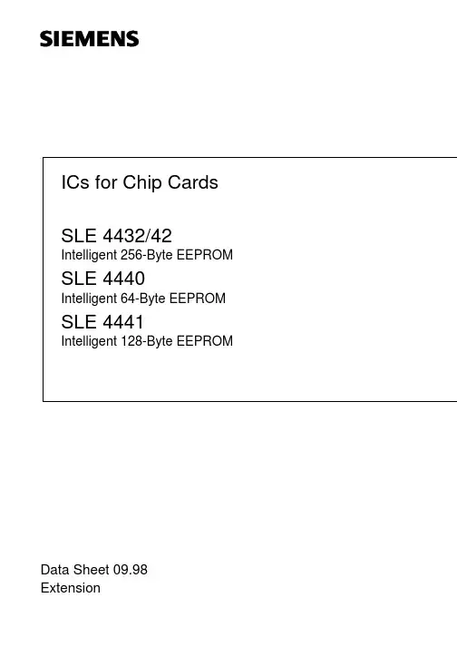
ICs for Chip CardsSLE 4432/42Intelligent 256-Byte EEPROMSLE 4440Intelligent 64-Byte EEPROMSLE 4441Intelligent 128-Byte EEPROMData Sheet 09.98ExtensionSLE 4432/40/41/42 Data Sheet ExtensionRevision History:Original Version 09.98Previous Releases:Page Subjects (changes since last revision)Important:For further information please contact:Siemens Semiconductor Group in Munich, Germany,Security & Chip Card ICs,Fax +49 89 636-22360The supply of this component does not include a license for its use in smartcard applications. This license is due to INNOVATRON Patents137 Boulevard de Sébastopol, 75002 Paris, France, Fax +33 1 4013 3909 Published by Siemens AG, Bereich Halbleiter, HL CC Applications Group Balanstr. 73, D-81541 München© Siemens AG 1998. All Rights Reserved.Attention please!As far as patents or other rights of third parties are concerned, liability is only assumed for components, not for applications, processes and circuits implemented within components or assemblies.The information describes the type of component and shall not be considered as assured characteristics.Terms of delivery and rights to change design reserved.For questions on technology, delivery, and prices please contact the Semiconductor Group Offices in Germany or the Siemens Companies and Representatives world-wide (see address list).Due to technical requirements components may contain dangerous substances. For information on the types in question please contact your nearest Siemens Office, Semiconductor Group.Siemens AG is an approved CECC manufacturer.PackingPlease use the recycling operators known to you. We can also help you – get in touch with your nearest sales office. By agreement we will take packing material back, if it is sorted. You must bear the costs of transport.For packing material that is returned to us unsorted or which we are not obliged to accept, we shall have to invoice you for any costs incurred.Components used in life-support devices or systems must be expressly authorized for such purpose!Critical components1) of the Semiconductor Group of Siemens AG, may only be used in life-support devices or systems2) with the express written approval of the Semiconductor Group of Siemens AG.1) A critical component is a component used in a life-support device or system whose failure can reasonably beexpected to cause the failure of that life-support device or system, or to affect its safety or effectiveness of that device or system.2)Life support devices or systems are intended (a) to be implanted in the human body, or (b) to support and/ormaintain and sustain human life. If they fail, it is reasonable to assume that the health of the user may beSLE 4441Intelligent 256-Byte EEPROM with Write Protect Function SLE 4432Intelligent 256-Byte EEPROM with Write Protect Function SLE 4442and Programmable Security Code (PSC)Features• 256 x 8-bit EEPROM organization • Byte-wise addressing• Irreversible byte-wise protection of lowest 32 addresses(Byte 0...31)• 32 x 1-bit organization of protection memory • Two-wire link protocol• End of processing indicated at data output • Ambient temperature T A -35... +80°C • Supply voltage 5 V −5 / +10 %• Supply current < 10 mA• EEPROM programming time 5 ms• ESD protection typical 4000 V• Endurance minimum 105 write/erase cycles / bit 1)•Data retention for minimum of 10 years 1)•Contact configuration and Answer-to-Reset (synchronous transmission) in accordanceto ISO standard 7816A dditional Feature of SLE 4442• Data can only be changed after entry of the correct 3-byte programmable security codeT ypeO rdering Code P ackageS LE 4432 M3o n request W ire-Bonded Module M3S LE 4432 Co n requestChipS LE 4442 M3o n request W ire-Bonded Module M3S LE 4442 Co n requestC hipSLE 4441I ntelligent 64-Byte EEPROM with Write Protect Function SLE 4440and Programmable Security Code (PSC)I ntelligent 128-Byte EEPROM with Write Protect Function SLE 4441and Programmable Security Code (PSC)• 64 x 8-bit EEPROM organization (SLE 4440)• 128 x 8-bit EEPROM organization (SLE 4441)• Byte-wise addressing• Irreversible byte-wise protection of lowest 32 addresses(Byte 0...31)• 32 x 1-bit organization of protection memory • Two-wire link protocol• End of processing indicated at data output • Ambient temperature T A -35... +80°C • Supply voltage 5 V −5 / +10 %• Supply current < 10 mA• EEPROM programming time 5 ms• ESD protection typical 4000 V• Endurance minimum 105 write/erase cycles / bit 1)• Data retention for minimum of 10 years 1)• Contact configuration and Answer-to-Reset (synchronous transmission) in accordance to ISO standard 7816• Data can only be changed after entry of the correct 3-byte programmable security codeT ype O rdering Code P ackageS LE 4440 M3o n request W ire-Bonded Module M3S LE 4440 Co n requestC hipS LE 4441 M3o n request W ire-Bonded Module M3S LE 4441 Co n requestC hipSLE 4441I ntroductionT his document describes changes and extensions of the Data Sheet 07.95 of SLE 4432 / SLE 4442. All information of the Data Sheet 07.95 are also valid for SLE 4440 and SLE 4441 (e.g. operational information) except the data mentioned in this document.I n detail the following items are added or changed•Memory size SLE 4440•Memory size SLE 4441•Ambient temperature T A –35°C…+80°C•ESD protection min. 1500 V, typical 4000 V•Endurance minimum 100000write/erase cycles / bit•Package: Module M3•Coding informationE specially the transmission protocol (2-wire) and commands are fully compatible for all chip types.1.Memory OverviewT he memory is organized in a Main Memory of•64 byte for SLE 4440•128 byte for SLE 4441•256 byte for SLE 4432 and SLE 4442E ach of the first 32 bytes of the Main Memory can be irreversibly protected against data change by writing the corresponding bit in the Protection Memory (32 bit). Dependent on the state of the protection bit the memory is read only (ROM) or may be erased and written again (EEPROM). Change of the manufacturer code is only possible by the chip manufacturer.C hange of data of the Main Memory and write a bit of the Protection Memory is only possible after a correct verification of the P rogrammable S ecurity C ode (PSC) for SLE 4440, SLE 4441 and SLE 4442.SLE 4441F igure 1Memory Overview SLE 4432SLE 4441F igure 3Memory Overview SLE 4440SLE 44412.CodingS LE 4432, SLE 4442, SLE 4440 and SLE 4441 are delivered with a customer related unique code in order to allow an unambiguous identification of the application. Thus a terminal can clearly accept or reject a card after reading the Answer-to-Reset and the identification data. The Answer-to-Reset (ATR) for synchronous IC cards according to ISO/IEC 7816 is a standardized procedure allowing to identify an IC card (ICC) supporting the synchronous Answer-to-Reset. The Answer-to-Reset data allow an interface device to select the appropriate chip type and operate the ICC according to the data sheet of the chip.T wo different coding schemes apply•Extended coding using encoded BER-TLV data objects according to ISO/IEC 7816-4•16-bit manufacturer code registered at Pro ElectronB oth schemes identify the application by the registered application provider identifier RID according to ISO/IEC 7816-52.1.Registered Application Provider Identifier RIDT he application is generally identified by the customer specific 5-byte registered application provider identifier RID according to ISO/IEC 7816-5 using the registration category values ‘A’ and ‘D’. The RID is a part of the AID. Thus the AID is constructed as following:A pplication identifier AIDR egistered application provider identifierRID (5 byte)P roprietary application provider identifier extension PIX (≤11 byte)•Registered application provider identifier RIDCustomer specific RID provided by the registration authority to the applicantR ID M eaning C omment‘A x xx xx xx xx’I nternational registration R ID is registered by Tele Denmark‘D c cc xx xx xx’N ational registration R ID is registered by a national authority ‘c cc’C ountry indicator C ountry code according to ISO 3166‘xx xx xx’A pplication provider sequence no.P rovided by national registration authority•Proprietary application provider identifier extension PIXExtension for the RID holder in order to diversify own applicationsA pplication forms for a RID are printed in the Annex A of ISO/IEC 7816-5.•For international registration one has to apply at the acting registration authority Tele Denmark for a RID indicated by ‘A’. The contact address is printed in ISO/IEC 7816-5•For national registration one has to apply at the relevant national standardization body or its acting registration authority for a RID indicated by ‘D’ followed by the country codeT he RID is provided by the customer to Siemens.SLE 44412.2.Extended Coding SchemeD ue to the available memory space the coding principle according to ISO/IEC 7816-4 applies for SLE 4432, SLE 4442, SLE 4440 and SLE 4441. Data are coded according to the ASN 1 data objects basic encoding rules using the structure Tag - Length - Value (BER TLV).F igure 5Structure of a Mono- Application Memory IC Card with a simple DIR-StructureT wo coding principles apply•Extended Coding Scheme (Compressed)H1H2H3H4T M L M I CM I CT T A L A R ID P IX•Extended Coding Scheme (according to German Health Insurance)H1H2H3H4T M L M I CM I CT…T T L T T A L A R ID P IXT he byte definition is explained in the following:A TR headerB yte H1:Protocol type = ‘A2’ indicating two-wire link protocolB yte H2:Protocol parameterB yte H3:Historical byte “Category Indicator” = ‘10’ indicating that the following byte H4 will be aDIR data referenceB yte H4:Historical byte “DIR data reference” = a pointer (byte address) to the first byte of thedirectory section (i.e. TA for Extended Coding Scheme - Compressed or TT forExtended Coding Scheme - according to German Health Insurance)SLE 4441A TR data sectionB yte TM:Tag manufacturing data object (‘pre-issuing data’) = ‘46’B yte LM:Length of manufacturing dataB yte ICM:IC manufacturer = ‘05’. For existing applications ICM = ’81’ is still availableB yte ICT:IC TypeD IR data sectionT he DIR data section contains according to ISO/IEC 7816-5 data objects for application selection. The following variants are possible:•The IC card is a mono application card and only the data object ‘application identifier’ (tag TA = ‘4F’) is present in the DIR data section. È Extended Coding Scheme (Compressed)•The IC card is a mono application card with the data object ‘application template’ (tag TT = ‘61’) in the DIR data section. The application template can contain along with the application identifier (tag TA = ‘4F’) further data objects (e.g. application label - tag ‘50’ or discretionary data - tag ’53’). È Extended Coding Scheme (according to German Health Insurance)N ote: Bytes H1, H2, H3, H4, ICM, ICT and the customer specific RID are programmed by Siemens and protected against further changes.2.3.16-bit Coding SchemeF or applications requiring only a unique coding the following construction applies2 byte1 byte5 byteM anufacturer Code M anufac-turer data R egistered application provideridentifier RID•Manufacturer Code registered at Pro Electron16-bit code provided by Siemens, fix for SLE 4432, SLE 4442, SLE 4440 and SLE 4441• Manufacturer dataDifferentiation of chip types SLE 4432, SLE 4442, SLE 4440 and SLE 4441•Registered application provider identifier RIDCustomer specific RID provided by the registration authority to the applicantNote: The above mentioned 8 bytes are programmed by Siemens and protected against further changes.SLE 44412.4.Codes OverviewSLE 4432, SLE 4442, SLE 4440 and SLE 4441 are available with the coding schemes.Please note that according to ISO/IEC 7816-6 Amendment 1 ICM = ‘05’ for new implementations. For existing applications ICM =’81’ is still available. It is recommended that terminals accept both IC manufacturer codes.Address012345678910…1415(dec)Address0123456789A…E F(hex)Meaning H1H2H3H4TM LM ICM ICT TA LA RID PIXData A2131088460205054F RID SLE 4432Data A2131088460205154F RID SLE 4442Data A2031088460205174F RID SLE 4440Data A20B1088460205164F RID SLE 4441 Figure 6Extended Coding Scheme (compressed)Address01234567…1718192021…2526(dec) Address01234567…1112131415…191A(hex) Meaning H1H2H3H4TM LM ICM ICT TT LT TA LA RID PIXData A21310910505RID SLE 4432 Data A21310910515RID SLE 4442 Data A20310910517RID SLE 4440 Data A20B10910516RID SLE 4441Figure 7Extended Coding Scheme (according to German Health Insurance)Address0123 (7)Meaning Manufacturer Code Manufac-turer data Registered application provideridentifier RIDData317401RID SLE 4432 Data317402RID SLE 4442 Data317404RID SLE 4440 Data317408RID SLE 4441Figure 816-bit Coding SchemeThe shaded bytes are programmed by Siemens and protected against further changes.SLE 4441 3.Operational Information3.1.Memory Map SLE 4440Main Memory Protection Memory Security MemoryAddress(decimal)64Data Byte 64 (D7 0::32Data Byte 32 (D7 031Data Byte 31 (D7...D0)Protection Bit 31 (D31):::4Data Byte 4 (D7...D0)Protection Bit 4 (D31)3Data Byte 3 (D7...D0)Protection Bit 3 (D3)Reference Data Byte 3 (D7 02Data Byte 2 (D7...D0)Protection Bit 2 (D2)Reference Data Byte 2 (D7 01Data Byte 1 (D7...D0)Protection Bit 1 (D1)Reference Data Byte 1 (D7 00Data Byte 0 (D7...D0)Protection Bit 0 (D0)Error CounterThe Data bytes 0 to 31 can be protected against further changes by programming the associated protection bit 0 to 31. The SLE 4440 allows data changing only after correct verification of the Reference Data bytes. Reading of the Data bytes and of the associated protection bits is always possible.3.2.Memory Map SLE 4441Main Memory Protection Memory Security MemoryAddress(decimal)128Data Byte 128 (D7 0::32Data Byte 32 (D7 031Data Byte 31 (D7...D0)Protection Bit 31 (D31):::4Data Byte 4 (D7...D0)Protection Bit 4 (D31)3Data Byte 3 (D7...D0)Protection Bit 3 (D3)Reference Data Byte 3 (D7 02Data Byte 2 (D7...D0)Protection Bit 2 (D2)Reference Data Byte 2 (D7 01Data Byte 1 (D7...D0)Protection Bit 1 (D1)Reference Data Byte 1 (D7 00Data Byte 0 (D7...D0)Protection Bit 0 (D0)Error CounterThe Data bytes 0 to 31 can be protected against further changes by programming the associated protection bit 0 to 31. The SLE 4441 allows data changing only after correct verification of the Reference Data bytes. Reading of the Data bytes and of the associated protection bits is always possible.SLE 44414.Electrical CharacteristicsThe listed characteristics are ensured over the operating range of the integrated circuit. Typical characteristics specify mean values expected over the production spread. If not otherwise specified, typical characteristics apply at T A = 25°C and the give supply voltage.4.1.Absolute Maximum RatingsStresses above those listed may cause permanent damage to the device. This is a stress rating only and functional operation of the device at these or any other conditions above those indicated in the operational sections of this data sheet is not implied. Exposure to absolute maximum rating conditions for extended periods may effect device reliability, including EEPROM data retention and write/erase endurance.Parameter Symbol Limit Values Unit Test Conditionmin.typ.max.ESD protection V S1*******V ISO/IEC 7816-1 Endurance 1)105—(write/erase cycles/bit)Data retention 1)10years—1)Values are temperature dependent, for further information please refer to your Siemens SalesOffice.4.2.Operation RangeParameter Symbol Limit Values Unit Test Conditionmin.typ.max.Ambient temperature T A-35+80°C—SLE 4441 5.PackageFigure 9Package Outlines Wire-Bonded Module M3。
MKP62(C42)规格承认书
0.6 C42Q2472-30****+++ 0.10M 17.5 9.5
2.2M 32.0 22.0 13.0 27.5 0.8 C42Q2225MBS****+++ 2.2K 32.0 25.0 13.0 27.5 0.8 2.2 2.7 3.3 32.0 16.0 22.0 27.5 0.8 32.0 28.0 14.0 27.5 0.8 32.0 30.0 16.0 27.5 0.8
d
0.0010 10.5 9.0 0.0012 10.5 9.0 0.0015 10.5 9.0 0.0018 10.5 9.0 0.0022 10.5 9.0 0.0027 10.5 9.0 0.0033 10.5 9.0 0.0039 10.5 9.0 0.0047 10.5 9.0 0.0056 10.5 9.0 0.0068 10.5 9.0 0.0082 10.5 9.0 0.010 10.5 9.0 0.012 10.5 9.0 0.015 10.5 9.0 0.018 10.5 9.0 0.022 10.5 9.0 0.027 10.5 9.0
地址: 中国厦门市海沧区新园路 99 号 外销
TEL: 0086-592-6208620 6208618 6208602 FAX: 0086-592-6208777 Mail: fsc@ michael_lai@ hhj@ Http:
C
直脚
D E M
软绝缘线(多股) 硬绝缘线(单股) 软绝缘线(多股) , 外壳带正底安装耳
T 3
P1=20.3mm±0.5m m P1=20mm±0.5mm
45
Page 4 of 11
MKP62
Code:C42
敏赛特技术有限公司产品说明书
Features•Normally closed “make or break” Klixon® contact system, which is operated by a snap action disc, is sensitive to both temperature and current.•Precision calibration – temperature calibrated and inspected under controlled conditions for dependable performance.•Automatic or manual reset series available •Easy to install•VDE certificate with production surveillance, overheating protector.37 amperes maximum locked rotor 230 VAC, File 4464.4-4510-1013,License No. 3938 UG for 3/4” M.P. only.•Inherent protection devices for approximately 1/2 to 5 h.p. motors used in applications such as industrial motors, agricultural equipment, well and sump pumps, fans, air conditioners, refrigerators, home appliances, etc.•When properly applied, protector shuts off motor when temperature exceeds maximum safe level due to an overload or stalled (locked rotor) condition.| SINGLE PHASE P HENOLIC MOTOR PROTECTORSHermetically Sealed Motor Protector for Single-Phase On-Winding Protection IntroductionKlixon Phenolic Motor Protectors are equipped with a bimetallic snap acting disc, on which the contacts are mounted, and through which the current flows. If overheating conditions occur, the heating effect of the current flow through the Klixon disc and the influence of motor heat will cause the disc temperature to rise.When the disc reaches the calibrated setpoint, the Klixon protector automatically opens and shuts down the motor, limiting the winding and shell temperature.When the motor has cooled to an acceptable operating level, allowing the protector to cool to its reset temperature, the Klixon protector resets automatically to a closed contact position allowing the motor to restart.Manual reset versions are also available for applications where automatic restarting may be hazardous to equipment or operations.Cover (Optional)Bimetal DiscHeater TerminalTerminalTerminalAdjusting ScrewPhenolic BaseSPECIFICATIONS DiagramsCurvesMetric Dimensions in ParenthesesDIMENSIONSRound BaseEared Base(Type ME 4-Holes. Type CE 2-Holes at #1Terminal End only. Other Types No Holes)ORDERING OPTIONSMaximum Recommended Protector Contact RatingsThis chart is used to determine protector size needed when making an application.Size Disc Contacts Terminals Max. CurrentV = 120Max. Current V = 2403/4”3/4”1”1”1”1”11/4”11/2”HCHCLCHCLCHCSTDSTDLCHCLCLCHCHCSTDSTD325040404080135175253730303060100130 HC = High Capacity LC = Low Capacity STD = Standard CapacityFor reference only. Please contact Sensata for application assistance.3/4”1”High Cap Low Cap High CapA B C D EJ L R ABADAEAFAGAHAIAJAKALAMAPFGJPLSOTABAEAFAGAHAIAJAKALAMANCDEHIKXAutomatic ResetOpen ±5°C Close ±9°CJKLVZNXYWUMRSH**P**O**= 90= 105= 105= 105= 120= 120= 120= 120= 135= 135= 135= 135= 135= 150**= 150**= 150**57**616978616978926169789210278**115**102**Manual ResetOpen ±5°C Close ±12°CGFABDE**= 90= 105= 105= 120= 135= 150**54**63***74*749696*** 1-Phase Protectors only.** Special temperatures.Consult net additions.*** 3-Phase Protectors only.Disc and Contact Operating TemperaturePage 7Sensata Technologies, Inc. (“Sensata”) data sheets are solely intended to assist designers (“Buyers”) who are developing systems that incorporate Sensata products (also referred to herein as “components”). Buyer understands and agrees that Buyer remains responsible for using its independent analysis, evaluation and judgment in designing Buyer’s systems and products. Sensata data sheets have been created using standard laboratory conditions and engineering practices. Sensata has not conducted any testing other than that specifically described in the published documentation for a particular data sheet. Sensata may make corrections, enhancements, improvements and other changes to its data sheets or components without notice.Buyers are authorized to use Sensata data sheets with the Sensata component(s) identified in each particular data sheet. HOWEVER, NO OTHER LICENSE, EXPRESS OR IMPLIED, BY ESTOPPEL OR OTHERWISE TO ANY OTHER SENSATA INTELLECTUAL PROPERTY RIGHT, AND NO LICENSE TO ANY THIRD PARTY TECHNOLOGY OR INTELLECTUAL PROPERTY RIGHT, IS GRANTED HEREIN. SENSATA DATA SHEETS ARE PROVIDED “AS IS”. SENSATA MAKES NO WARRANTIES OR REPRESENTATIONS WITH REGARD TO THE DATA SHEETS OR USE OF THE DATA SHEETS, EXPRESS, IMPLIED OR STATUTORY, INCLUDING ACCURACY OR COMPLETENESS. SENSATA DISCLAIMS ANY WARRANTY OF TITLE AND ANY IMPLIED WARRANTIES OF MERCHANTABILITY, FITNESS FOR A PARTICULAR PURPOSE, QUIET ENJOYMENT, QUIET POSSESSION, AND NON-INFRINGEMENT OF ANY THIRD PARTY INTELLECTUAL PROPERTY RIGHTS WITH REGARD TO SENSATA DATA SHEETS OR USE THEREOF.All products are sold subject to Sensata’s terms and conditions of sale supplied at SENSATA ASSUMES NOLIABILITY FOR APPLICATIONS ASSISTANCE OR THE DESIGN OF BUYERS’ PRODUCTS. BUYER ACKNOWLEDGES AND AGREES THAT IT IS SOLELY RESPONSIBLE FOR COMPLIANCE WITH ALL LEGAL, REGULATORY AND SAFETY-RELATED REQUIREMENTS CONCERNING ITS PRODUCTS, AND ANY USE OF SENSATA COMPONENTS IN ITS APPLICATIONS, NOTWITHSTANDING ANY APPLICATIONS-RELATED INFORMATION OR SUPPORT THAT MAY BE PROVIDED BY SENSATA.CONTACT USRevised 11/25/17Americas+1 (760) 597 7042**************************Europe, Middle East & Africa +1 (760) 597 7042**************************Asia Pacific*************************.com China +86 (21) 2306 1500Japan +81 (45) 277 7117Korea +82 (31) 601 2004India +91 (80) 67920890Rest of Asia +886 (2) 27602006 ext 2808APPLICATION WORKSHEETA sample worksheet provides the information needed for a proper application. It is not possible to apply a Klixon protector based on horsepower, amperage, or name plate data only.Motor DataA. Locked Rotor Requirements1. Locked Rotor Current Cold: the current which exists the instant the motor is turned on.2. Locked Rotor Current Hot: The current level that exists at end of 1st cycle test. Typically 10 to 30 seconds after motor is first turned on.3. Time elapsed during above test to raise motor winding temperature from room temperature to around maximum allowed temperature for the ULclass of motor insulation. An example would be, for a class A motor, 25ºC to 175ºC in 12.5 seconds.4. Ambient Temperature During test: Room temperature (usually 25ºC).B. Running Overload Requirements1. Load Current: With the motor running, the load on the motor is to be increased in small increments until the motor winding has completely stabilized at approximately 10ºC below the maximum allowed by the UL class of the motor. An example would be, for a class A motor, the maximum allowed is 140øC. The motor winding temperature was completelystabilized at 130ºC and the current draw at that time would be recorded. 2&3. Protector Location Temperatures: These temperatures are taken at the conclusion of the above load current test while the motor is running under the above load.4. Ambient Temperature: Room temperature (usually 25ºC).C. Abnormal Conditions for Protection.1. Max/min Ambient Temperatures: temperature in the surroundings of protector.2. Max/min Line Volts: The highest and lowest voltages for which protection should be effective.3. Other environmental considerations: i.e., exposed to agricultural weather conditions.Name Plate DataA. HorsepowerB. VoltageC. Single or three phaseD. FLA (full load amps)E. LRA (locked rotor amps)F. Insulation class (UL/CSA) (indicate one)Protector RequirementsA. Automatic or manual resetB. Round or eared baseC. Termination typeMotor Data RequiredA. Locked rotor requirements 1. Locked rotor current cold 2. Locked rotor current hot3. Time required to raise motor winding to max. temperature4. Ambient temperature during test B. Running overload requirements1. Load current required to stabilize main winding temp. at 10ºC below maximum allowed2. Protector location temperature below protector surface3. Protector location temperature above protector (air temp)4. Ambient temp during testC. Abnormal conditions for protection 1. Max/min ambient temperatures 2. Max/min line volts3. Other environmental considerationsNote: Application assistance available from Sensata.H.P Volts Phase Amps Amps ABFHAmps Amps Sec DegAmps Deg Deg Deg Deg Volts。
sl6654中文资料_数据手册_IC数据表
FEATURESLow Power Consumption (1.5mA)Single Chip SolutionGuaranteed 100MHz Operation Exceptionally Stable RSSIAPPLICATIONSCellular Radio Telephones Cordless TelephonesQUICK REFERENCE DATASupply Voltage 2.5V to 7 5V Sensitivity 3µVCo-Channel Rejection 7dBSL6654LOWER POWER IF/AF CIRCUIT (WITH RSSI) FOR FM CELLULAR RADIOThe SL6654 is a complete single chip mixer/oscillator, IF amplifier and detector for FM cellular radio, cordless telephones and low power radio applications. It features an exceptionally stable RSSI (Received Signal Strength Indicator) output using a unique system of detection. Supply current is less than 2mA from a supply voltage in the range2.5V to 7.5V.Fig. 1 Pin connections (top view)MP18Fig. 2 block diagramDS 3286 -1SL6654 IS FOR MAINTENANCE PURPOSES ONLY AND IS NOT RECOMMENDED FOR NEW DESIGNSSL6654ABSOLUTE MAXIMUM RATINGSSupply voltage8VStorage temperature -55°C to +150°C Operating temperature -55°C to +125°CMixer input1V rmsELECTRICAL CHARACTERISTICSTest conditions (unless otherwise stated):V = 2.5V to 7.5V, T = -30°C to +85°C, IF = 455kHz, RF = 50MHz, Quad Coil Working Q = 30NOTES1.The RSSI output is 100% dynamically tested at 5V and +20° C over a 70dB range. First the input to pin 14 is set to2.5mV and the RSSI current recorded Then for each step of 10dB from -40 to +30dB the current is measured again. The current change in each step must meet the specified figure for current change. The RSSI output is guaranteed monotonic and free from discontinuities over this range.2.Co-channel rejection is measured by applying a 3kHz deviation, 1 kHz modulated signal at an input level to give a 20dB SINAD ratio. Then a 3kHz deviation, 400Hz modulated signal on the same frequency is also applied and its level increased to degrade the SINAD to 14dB.9015002045575Diff. input impedance Audio output level 125dB kHz kohmmVSL6654Fig. 3 Internal schematicGENERAL DESCRIPTIONThe SL6654 is a very low power, high performance integrated circuit intended for IF amplification and demodulation in FM radio receivers. It comprises:q A mixer stage for use up to lOOMHzq An uncommitted transistor for use as an oscillatorq A current sink for biasing this transistorq A limiting amplifier operating up to 1.5MHzq A quadrature detector with differential AF outputq An RSSI (Received Signal Strength Indicator) output MixerThe mixer is single balanced with an active load. Gain is set externally by the load resistor although the value is normally determined by that required for matching into the ceramic filter. It is possible to use a tuned circuit but an increase in mixer gain will result in a corresponding reduction of the mixer input intercept point.The RF input is a diode-biased transistor with a bias current of typically 300µA. The oscillator input is differential but would normally be driven single-ended. Special care should be taken to avoid accidental overload of the oscillator input.OscillatorThe oscillator consists of an uncommitted transistor and a separate current sink. The user should ensure that the design of oscillator is suitable for the type of crystal and frequency required; it may not always be adequate to duplicate the design shown in this data sheet.IF amplifierThe limiting amplifier is capable of operation to at least 1 MHz and the input impedance is set by an external resistor to match the ceramic filter. Because of the high gain, pins 12 and 13 must be adequately bypassed.DetectorA conventional quadrature detector is fed internally from the IF amplifier; the quadrature input is fed externally using an appropriate capacitor and phase shift network. A differential output is provided to feed a comparator for digital use, although it can also be used to provide AFC.RSSI outputThe RSSI output is a current source with value proportional to the logarithm of the IF input signal amplitude. There is a small residual current due to noise within the amplifier (and mixer) but beyond this point there is a measured and guaranteed 70dB dynamic range. The typical range extends to 92dB, independent of frequency, and with exceptionally good temperature and supply voltage stability.SL6654Supply voltageThe SL6652 will operate reliably from 2.5V to 7.5V The supply line must be decoupled with 470nF using short leads.DetectorThe internal band gap reference must be externally decoupled. It can be used as an external reference but must not be loaded heavily; the output impedance is tyically 14ohms.Fig. 4 Audio output vs input and temperature at 2.5VFig. 5 Audio output vs input and temperature at 5.0V Fig. 6 Audio output vs input and temperature at +7.5V Fig. 7 Audio output vs input and supply voltage at +25°C Fig. 8 SINAD and input level Fig. 9 AM rejection and input levelSL6654Fig. 10 RSSI output vs input and supply voltage(Tamb = 20°C)Fig. 11 RSSI output vs input level and temperature(VCC= 2.5V)Fig. 12 RSSI output vs input level and temperature(TCC = 5V)Fig. 13 RSSI output vs input level and temperature(VCC= 7.5V)SL6654Fig. 14 Signal + noise to noise ratio vs input level Fig. 15 Supply current vs supply voltage= 5V)Fig. 16 Supply current vs temperature (VCC。
SLE66CLX320P_datasheet
Security & Chip Card ICsSLE 66CLX320P16-Bit High Security Dual Interface ControllerISO/IEC 7816 and 14443 Type A & B Compliant Interfaces For Contact and Contactless Operationwith Memory Management and Protection Unitin 0.22 µm CMOS Technology136-Kbyte ROM, 5-Kbyte RAM, 32-Kbyte EEPROM1100-Bit Advanced Crypto Enginesupporting RSA and Elliptic Curve GF(p)112-Bit / 192-Bit DDES-EC2 Acceleratorsupporting DES, 3DES and Elliptic Curve GF(2n)SLE 66CLX321P Short Product Information Ref.: SPI_SLE66CLX320P_0404.doc This document contains preliminary information on a new product under development. Details are subject to change without notice.Revision History: Current Version 2004-04-01Previous Releases: 2004-02-12Page4 Type A baud rate support of 106kbit/sImportant: Further information is confidential and on request. Please contact:Infineon Technologies AG in Munich, Germany,Security & Chip Card ICs,Tel +49 - (0)89 234-80000Fax +49 - (0)89 234-81000E-Mail: security.chipcard.ics@Published by Infineon Technologies AG, SMS Security Applications GroupSt.-Martin-Strasse 53, D-81541 München© Infineon Technologies AG 2004All Rights Reserved.To our valued customersWe constantly strive to improve the quality of all our products and documentation. We have spent an exceptional amount of time to ensure that this document is correct. However, we realise that we may have missed a few things. If you find any information that is missing or appears in error, please use the contact section above to inform us. We appreciate your assistance in making this a better document.Attention please!The information herein is given to describe certain components and shall not be considered as warranted characteristics.Terms of delivery and rights to technical change reserved.We hereby disclaim any and all warranties, including but not limited to warranties of non-infringement, regarding circuits, descriptions and charts stated herein.Infineon Technologies is an approved CECC manufacturer.InformationFor further information on technology, delivery terms and conditions and prices please contact your nearest Infineon Technologies Office in Germany or our Infineon Technologies Representatives world-wide (see address list).WarningsDue to technical requirements components may contain dangerous substances. For information on the types in question please contact your nearest Infineon Technologies Office.Infineon Technologies Components may only be used in life-support devices or systems with the express written approval of Infineon Technologies, if a failure of such components can reasonably be expected to cause the failure of that life-support device or system, or to affect the safety or effectiveness of that device or system. Life support devices or systems are intended to be implanted in the human body, or to support and/or maintain and sustain and/or protect human life. If they fail, it is reasonable to assume that the health of the user or other persons may be endangered.16-Bit High Security Dual Interface ControllerISO/IEC 7816 and 14443 Type A &B Compliant InterfacesFor Contact and Contactless Operation with MMU in 0.22 µm CMOS Technology 136-Kbyte ROM, 5-Kbyte RAM, 32-Kbyte EEPROM1100-Bit Advanced Crypto Engine supporting RSA and Elliptic Curve GF (p) and 112-Bit / 192-Bit DDES-EC2 Acceleratorsupporting DES, 3DES and Elliptic Curve GF (2n)Features•Enhanced low power 8051 CPU with extended addressing modes for dualinterface smart card applications •Instruction set opcode compatible with standard 8051 processor with additionalpowerful instructions optimized for smartcard application•Enhanced architecture with execution time6 times faster (18 times usingPLLmax) than standard 8051 processor at same external clock•134 Kbytes User ROM for operating system and application (programs & data)• 2 Kbytes reserved ROM for Resource Management System (RMS_E) withContactless Optimized EEPROMwrite/erase routines•32 Kbytes Secure EEPROM inSuperSlim technology for applicationprogram and data•4k bytes XRAM, 700 bytes Crypto-RAM and 256 bytes internal RAM for fast data processing•Memory Management Unit •Certified True Random NumberGenerator•Dual Key Triple DES (DDES) &GF(2n) Elliptic Curve (EC2) Accelerator •Advanced Crypto Engine for Elliptic Curve GF(p) and up to 2048 bits RSAcomputation•CRC Module according to ISO/IEC 3309 supporting CCIT v.41 & HDLC X25•8 Interrupt Vectors Module with 3 priority levels to ensure real time operation •PLL: to speed up the internal CPU clock frequency up to 15MHz (optional use)•Two 16-bit Timers with interrupt capability for protocols, security checks & watch dog implementations•Power saving sleep mode •Temperature range:contact-based: -25°C to +85°Ccontact-less: -25°C to +70°CFull operation either via Contact-based and/or Contactless interfaces controlled by Operating System enhances Security LevelContact-based Interface•Contact configuration and serialinterface according to ISO/IEC 7816 •UART handling serial interface compliant with ISO/IEC 7816 supportingtransmission protocols T=0 and T=1•Supply voltage range:5V ± 10% (Class A)3V ± 10% (Class B)•Current consumption < 10 mA @ 5.5 V •External CPU clock frequency:1 to 7.5 MHz•Internal CPU clock frequency:up to 15 MHz•ESD protection larger than 6 kVContactless Interface•Interface according to ISO/IEC 14443 for both Type A and Type B•Carrier frequency 13.56 MHz•Data rate106 Kbit/s in type A operationup to 848 Kbit/s in type B operation •Anticollision & Transmission Protocol supported by open source applicationnotes for both Type A & B •Flexible Internal CPU clock frequency: fully configurable from 1.7MHz up to15 MHz•256 bytes buffer for contactless data exchange (FiFo circular architecture) •Parallel operation of CPU, Peripherals like DES, CRC and Contactless Interface possible for High DemandingContactless Applications EEPROM (SuperSlim Technology) •Byte wise EEPROM programming and read accesses•Versatile & Flexible page mode for 1 to 256 bytes write/erase operation•32 bytes security area including:- 16 bytes chip unique identification number - 16 bytes PROM area (OTP like) •Fast personalisation mode 1.5 ms •Typical Page Erase time < 2.5ms •Typical Page Writing time < 1.8 ms •Minimum of 100.000 Write/erase cycles1)•Data retention for a minimum of 10 years1)•EEPROM programming voltage generated on chipMemory Management and Protection Unit•Addressable memory up to 1 Mbytes •Separates OS (system mode) andApplication (application mode) •System routines called by traps •Access Restrictions to peripherals in application mode controlled by OS •Code execution from XRAM possible1) Values are temperature dependantSecurity FeaturesOperation state monitoring mechanism The chip goes in a secure reset state on any following sensors alarm:•Low and high voltage sensors •Internal voltage sensor •Frequency sensors and filters•Light sensor•Glitch sensor•Temperature sensor•Life Test Sensor•Internal power-on reset sensor •Active Shield with automatic and user controlled attack detectionSecure chip and firmware design •Security scrambled & optimized chip layout against physical chip manipulation •Memory encryption/decryption module (MED) for XRAM, ROM and EEPROMagainst reverse engineering and powerattacks•ROM code not visible due to implantation •Mask dependant ROM code encrypted during production•Chip Unique encryption of the XRAM and EEPROM•Flexible encryption of part or whole EEPROM by additional user-defined key •16 byte Unique chip identification number for anti-clone countermeasure & tracking •16 bytes security PROM hardware protected (OTP like)•Secure start of the operating system ensured by certified Self Test Software(STS)•Certified EEPROM programming routines (RMS_E)•True Random Number Generator with Firmware test function•High Speed SPA/DPA resistant Triple DES (DDES) Accelerator and AdvancedCrypto Engine Anti Snooping•HW-countermeasures against SPA/DPA-, Timing- and DFA-attacks (differential fault analysis)Supported Standards•ISO/IEC 7816•EMV 2000•GSM 11.1x•ETSI TS 102 221•ISO/IEC 14443•ISO/IEC 3309•CCIT v.41•HDLC X25Application Support•HW-& SW-Tools (Emulator, ROM Monitor, Card Emulator, Simulator, Evaluation Kit Proximity (Contactless Reader package), SmartMask™ package, Simulated Reader Software, etc.)•Open Source Application Notes Tutorial(e.g.: T=0, T=1, DES and 3DES, CryptoLibrary, Anticollision and ContactlessTransmission Protocols for both Type Aand B, Card Coil Design Guide, Card Coil Antenna Reference Design List, etc.) •Certified CC EAL5+ Crypto Library •Worldwide Application Engineer Team and customer dedicated Field ApplicationEngineers•Regular Customer trainings onCryptography, Contactless and Dualinterface controllers including ISO/IEC14443 related topics•On-site trainings available on requestDocument References •Confidential Data Book SLE 66CxxP •Confidential Instruction Set SLE 66CxxP •Confidential Quick Reference SLE 66CxxP •Chip Qualification report•Chip delivery specification for wafer with chip-layout (die size, orientation, ...) •Module specification containing description of package, etc.•Module Qualification reportDevelopment Tools Overview •Software Development Kit SDK CC •Card Emulator CE66P Dual Interface •ROM Monitor RM66P-II with stand alone functionality for ROM mask qualification in the end user system•Emulator ET66P Hitex or ET66P KSC •Smart Mask™ Package for chip evaluation •Smart Mask™ Dual Interface modules M8.4 (supplied by Infineon) supporting both ISO/IEC 14443 Type A & B and ISO/IEC7816 for implantation process testing andproduction setup•Evaluation Kit Proximity (Contactless reader package)Timing performances are independent of the contact or contactless interface.Table 1 Performance Advanced Crypto EngineOperation Modulus ExponentCalculation Time at 5 MHz Calculation Time at15 MHzModular Exponentiation 160 bit 160 bit 20 ms 7 ms Modular Exponentiation 256 bit 256 bit 35 ms 12 ms Modular Exponentiation512 bit 512 bit 110 ms 37 ms Modular ExponentiationRSA Encrypt / RSA Signature Verify 1024 bit 16 bit 20 ms 7 ms Modular ExponentiationRSA Decrypt / RSA Signature Generate 1024 bit1024 bit820 ms273 ms Modular Exponentiation using CRTRSA Decrypt / RSA Signature Generate eq.1024 bit eq.1024 bit 250 ms 83 ms DSA Signature Generate 512 bit 160 bit 145 ms 48 ms DSA Signature Verify 512 bit 160 bit 130 ms 43 ms DSA Signature Generate 1024 bit 160 bit 290 ms 97 ms DSA Signature Verify1024 bit 160 bit 360 ms 120 ms Elliptic Curves EC-GDSA Sign. Generate 160 bit160 bit 260 ms 87 ms Elliptic Curves EC-GDSA Sign. Verify. 160 bit160 bit550 ms183 msFeatures (cont’d)Table 2Performance DDES-EC2 AcceleratorEncryption Time for an 8-byte Block including Data TransferOperation Data BlockLength5 MHz15 MHz High Speed and Secure 56-bit Single DES Encryption (incl. key loading) 64 bit 37 µs 12 µs High Speed and Secure56-bit Single DES Encryption64 bit23 µs 8 µs High Speed and Secure 112-bit Triple DES Encryption (incl. key loading)64 bit 60 µs 20 µs High Speed and Secure112-bit Triple DES Encryption 64 bit 35 µs12 µsCalculation TimeOperand Length5 MHz 15 MHz Elliptic Curves GF(2n ) EC-DSA Signature Generate 192 bit 285 ms 95 ms Elliptic Curves GF(2n ) EC-DSA Signature Verify 192 bit540 ms180 msTable 3 Ordering Information 1Type Package Voltage Range TemperatureRange Frequency Range (external clock) SLE 66CLX320P – M8.4 M8.42 SLE 66CLX320P – C Chip2.7 V - 5.5 V– 25°C to + 85°C1 MHz – 7.5 MHz1 Ordering Codes are available on request 2Dual Interface Module (M8.4)Pin DescriptionC1C5C2C6C3C7C4C8 Figure 1 M8.4 Pin Configuration Wire-bonded Module (top view)Figure 2 Pad Configuration (die)Table 4 Pin Definitions and FunctionsCard Contact Symbol FunctionvoltageC1 VDDSupplyinputC2 RSTResetC3 CLK Processor clock inputGroundC5 GNDC7 I/O Bi-directional data portLA Coil connection pin LALB Coil connection pin LBGeneral DescriptionThe dual interface security controller SLE 66CLX320P is a member of the Infineon Technologies SLE 66CxxxP high-end security controller family in 0.22 µm CMOS technology which is designed for security systems that requires continuous ongoing improvements with the highest degree of protection against fraudulent attacks.SLE 66CLX320P is targeting dual interface smart card applications such like national ID cards, banking, security access, digital signature and transport..SLE 66CLX320P offers 134 Kbytes of User-ROM, 256 bytes internal RAM, 4 Kbytes XRAM, 700 bytes Crypto RAM and 32 Kbytes EEPROM, which can be used as data and as program memory. The non-volatile memory consists of high reliability cells to guarantee data integrity. This is especially important when the EEPROM is used as program memory.It features ISO/IEC 14443 Type A and B contactless interfaces as well as an ISO/IEC 7816 contact-based interface on a single chip that can be operated in parallel. It also supports symmetric and asymmetric public-key algorithm such like DES, 3DES, Elliptic Curves and RSA independently of the communication mode.Figure 2: Block Diagram of SLE 66CLX320PThe CPU provides the high efficiency of the 8051 instruction set extended by additional powerful instructions with enhanced performance, memory sizes and security features tailored for contact and contactless smart card applications. Using the embedded PLL, the internal clock is adjustable up to 15 MHz independent from the carrier frequency of the magnetic field supplied by the contactless terminal.The Memory Management Unit allows a secure separation of the operating system and the applications. Using the system/application mode, it allows to securely downloading applications in the field after card personalisation. Using the MMU transparent mode allows keeping the memory mapping for code compatibility to SLE 66CxxS family. These new features suit the requirements of the new generation of operating systems.The UART supports the half-duplex transmission protocols T=0 and T= 1 according to ISO/IEC 7816-3. All relevant transmission parameters can be adjusted by software, as e.g. the clock division factor, direct/inverse convention and the number of stop bits. Additionally, the I/O port can be driven by communication routines realized in software. To minimize the overall power consumption, the smart card controller can be set into sleep mode supporting clock stop mode. Timers ease the implementation of advanced communication protocols such as T=CL (according to ISO/IEC 14443-4) and all other time critical processes for contactless communications. Both Timers features auto-reload mechanisms as well as their own dedicated interrupt vectors. Additional interrupts capability of the RF interface module allows real time operation of the pure contactless smart card with the contactless terminals.SLE 66CLX320P is able to communicate with any Proximity Card Device (PCD) defined in ISO/IEC 14443 such as the Infineon Evaluation Kit Proximity over a typical coupling distance of 10 cm. The power supply and data are received by an antenna, which consists of a coil with a few turns directly connected to the IC. DES acceleration by a factor of more than 500 compared to software solutions in combination with the high data transfer rate up to 848 Kbit/s keep the transaction times short. For more independence and flexibility, the controller offers the two modulation type A and type B according ISO/IEC 14443.The Anticollision and Contactless Transmission Protocol are supported by open source application notes for both Type A and B in order to offer a maximum flexibility to the Operating System. Both Contactless Communication protocol may be implemented in the Operating System while the final selection of the Type A or B is based upon the personalisation data of the contactless smart card. The communication type can also be changed during runtime in the field. Thus, SLE 66CLX320P ensures a simplified handling of the ROM mask, high reactivity by a tailored personalisation during production of the contactless smart card in order to answer to the increasing market demand and applications.SLE 66CLX320P features a new Resource Management System (RMS_E) which optimizes Contactless EEPROM write/erase routines. EEPROM programming is enhanced over the entire communication distance compared to the standard RMS. Thus, the reduction of programming times and power consumption is ensured independently of the use of the contact or the contactless interface.The CRC module allows the easy generation of checksums according to ISO/IEC 3309 (16-Bit-CRC), thus it supports the two different CRC calculation required for ISO/IEC 14443 Type A and Type B. Also, data as well as program located in the EEPROM can be extra-secured by a CRC checksum enabling the Operating System to detect errors while downloading new application in the field.To minimize the overall power consumption, the pure contactless smart card controller can be set into sleep mode.The certified random number generator (RNG) is able to supply the CPU with true random numbers on all conditions. It allows creating session key used for authentication in open networks and enable secure downloading of new applications.The DDES-EC2 accelerator consists of two modules.The DDES module supports symmetrical crypto algorithms according to the Data Encryption Standard in the Electronic Code Book Mode. It features two internal registers for storage of the two keys required for a Triple DES computation. Together with the fast contactless interface, it offers high security and high speed for dual interface smart card applications.The EC2 module accelerates the multiplication in GF (2n) and therefore the operations for elliptic curve cryptography. It widens the field of application for SLE 66CLX320P since it can be used as tamper-resistant security tool for secured and authentic communication in open networks.The Advanced Crypto Engine (ACE) is equipped with its own RAM of 700 bytes and supports all of today known public-key algorithms based on large integer modular arithmetic. It allows fast and efficient calculation of e.g. RSA operations with key lengths up to 2048 bit and Elliptic Curve GF (p).As an important feature, SLE 66CLX320P provides a new and enhanced level of on-chip security, which fulfils the strong security requirements of a Common Criteria evaluation at an EAL5 level. Each security measure is designed to act as an integral part of the complete system in order to strengthen the system as a whole.Thus, porting an existing Operating System to SLE 66CLX320P requires only very limited changes as it is typically reduced to add the Contactless Library and the Contactless Optimized Resource Management System (RMS_E) to the existing Operating System.SLE 66CLX320P integrates outstanding memory sizes, additional peripherals in combination with enhanced performance and optimized power consumption on a minimized die size.In conclusion, SLE 66CLX320P fulfils the requirements of for both contact-based and contactless smart card applications such like national ID card, banking, security access, digital signature and transport. In the case a pure contactless security controller is required, SLE 66CLX321P offers a solution without the contact-based interface of the SLE 66CLX320P.。
- 1、下载文档前请自行甄别文档内容的完整性,平台不提供额外的编辑、内容补充、找答案等附加服务。
- 2、"仅部分预览"的文档,不可在线预览部分如存在完整性等问题,可反馈申请退款(可完整预览的文档不适用该条件!)。
- 3、如文档侵犯您的权益,请联系客服反馈,我们会尽快为您处理(人工客服工作时间:9:00-18:30)。
Security & Chip Card ICsSLE 66C42P16-Bit Security Controllerwith Memory Management and Protection Unitin 0.22 µm CMOS Technology64-Kbyte ROM, 2304 bytes RAM, 4-Kbyte EEPROM 112-Bit / 192-Bit DDES-EC2 AcceleratorShort Product Information 11.02SLE 66C42P Short Product Information Ref.: SPI_SLE 66C 42P_1102 This document contains preliminary information on a new product under development. Details are subject to change without notice.Revision History:Current Version 11.02Previous Releases:0202Page Subjects (changes since last revision)3,4Important:Further information is confidential and on request. Please contact:Infineon Technologies AG in Munich, Germany,Security & Chip Card ICs,Tel :+49 89 234-80000Fax +49 89 234-81000E-Mail:security.chipcard.ics@Edition 2002Published by Infineon Technologies AG, CC Applications GroupSt.-Martin-Strasse 53, D-81541 München© Infineon Technologies AG 2001All Rights Reserved.Attention please!The information herein is given to describe certain components and shall not be considered as warranted characteristics.Terms of delivery and rights to technical change reserved.We hereby disclaim any and all warranties, including but not limited to warranties of non-infringement, regarding circuits, descriptions and charts stated herein.Infineon Technologies is an approved CECC manufacturer.InformationFor further information on technology, delivery terms and conditions and prices please contact your nearest Infineon Technologies Office in Germany or our Infineon Technologies Representatives world-wide (see address list).WarningsDue to technical requirements components may contain dangerous substances. For information on the types in question please contact your nearest Infineon Technologies Office.Infineon Technologies Components may only be used in life-support devices or systems with the express written approval of Infineon Technologies, if a failure of such components can reasonably be expected to cause the failure of that life-support device or system, or to affect the safety or effectiveness of that device or system. Life support devices or systems are intended to be implanted in the human body, or to support and/or maintain and sustain and/or protect human life. If they fail, it is reasonable to assume that the health of the user or other persons may be endangered.16-Bit Security Controller with MMU in 0.22 µm CMOS Technology 64-Kbyte ROM, 2304 bytes RAM, 4-Kbyte EEPROM112-Bit / 192-Bit DDES-EC2 AcceleratorFeatures•16-bit microcomputer in 0.22 µm CMOS technology•Instruction set opcode compatible with standard SAB 8051 processor •Enhanced 16-bit arithmetic •Additional powerful instructions optimized for chip card applications •Dedicated, non-standard architecture with execution time 6 times faster (18 times by PLLmax) than standard SAB 8051processor at same external clock•62 Kbytes User ROM for application programs•Additional 2 Kbytes reserved ROM for Resource Management System (RMS+Superslim) with intelligent EEPROMwrite/erase routines• 4 Kbytes Superslim-EEPROM• 2 Kbytes XRAM, 256 Bytes IRAM •Memory Management and Protection Unit (MMU)•Dual Key Triple DES (DDES) and EC2 GF (2n) Accelerator•CRC Module•Interrupt Module•Two 16-bit Autoreload Timer•PLL up to 15 MHz•Power saving sleep mode •External clock frequency 1 to 7.5 MHz for internal clock ≤ 15 MHz•UART for handling serial interface in accordance with ISO/IEC 7816 part 3supporting transmission protocols T=1 and T=0•I/O routines realized in software executable •Supply voltage range: 2.7 V to 5.5 V •Current consumption< 10mA @ 5.5 V< 6 mA @ 3.3 V •Temperature range: -25 to +85°C•ESD protection larger than 6 kVS uperslim-EEPROM•Reading and programming byte by byte •Flexible page mode for 1 to 64 bytes write/erase operation•32 bytes security area (OTP)•Fast personalization mode 0.63 ms •Erase + Write time < 4.0 ms @ 15 MHz •Minimum of 500.000 write/erase cycles at 25°C•Data retention for a minimum of 10 years •EEPROM programming voltage generated on chipM emory Management and Protection Unit •Addressable memory up to 1 Mbyte •Separates OS (system) and application (user)•System routines called by traps•OS can restrict access to peripherals in application mode•Code execution from XRAM possibleS ecurity FeaturesOperation state monitoring mechanism •Low and high voltage sensors •Frequency sensors and filters•Light Sensor•Glitch Sensor•Temperature Sensor•Life Test Function for SensorsTestmode•Irreversible Lock - Out of testmodeAnti Snooping•HW-countermeasures against SPA/DPA-, Timing- and DFA-attacks (differential fault analysis – DFA)•CRC - Module•Non standard dedicated Smart Card CPU - Core•Active Shield with automatic and user controlled attack detectionS upport•HW-& SW-Tools (Emulator, ROM Monitor, Card Emulator, Simulator, Softmasking)•Application notesSupported Standards•ISO/IEC 7816•EMV 96•GSM 11.11, 11.12, 11.18•ETS I TS 102 221Memory Security•16 bytes security PROM, hardwareprotected•Unique chip identification number for each chip•MED – memory encryption/decryption device for XRAM, ROM and EEPROM • True Random Number Generator with Firmware test function•Security optimised layout and layoutscrambling•user settable additional encryption key for EEPROMDocument References•Confidential Data Book SLE 66CxxxP •Qualification report•Chip delivery specification for wafer with chip-layout (die size, orientation,...)•Module specification containing description of package, etc.•Qualification report moduleDevelopment Tools Overview•Short Product Information Software Development Kit SDK CC•Short Product Information Card Emulator CE66P•Short Product Information ROM Monitor RM66P•Short Product Information Emulator ET66P Hitex or ET66P KSC•Short Product Information Smart Mask PackageFeatures (cont’d)Performance DDES-EC2 Accelerator Encryption Time for an 8-Byte Block incl. Data TransferOperationData Block Length5 MHz 10 MHz 15 MHz56-bit Single DES Exponentiation 64 bit 23 µs 11 µs 8 µs 112-bit Triple DES Exponentiation64 bit 35 µs17 µs12 µsCalculation Time Operand Length5 MHz 10 MHz 15 MHz Elliptic Curves GF(2n ) EC-DSA Signature Generate 192 bit 285 ms 142 ms 95 ms Elliptic Curves GF(2n ) EC-DSA Signature Verify192 bit540 ms 270 ms 180 msOrdering Information TypePackage 1VoltageRange Temperature RangeFrequency Range (ext. clock frequency)SLE 66C42P M5M5SLE 66C42P CDie2.7 V - 5.5 V or 1.62 V – 5.5 V – 25°C to + 70°C or– 25°C to + 85°C1 MHz - 5 MHzor1 MHz - 7.5 MHzFor ordering information please refer to the databook and contact your sales representative.Production sites:• Dresden (Germany) SLE 66CxxxP • UMC (Taiwan) SLE 66CxxxPU •Altis (France) SLE 66CxxxPA1available as wire-bonded module (M5) for embedding in plastic cards or as die (C) for customer packagingPin ConfigurationFigure 1: Pin ConfigurationPin Definitions and Functions Symbol FunctionVCC Operating voltage RST Reset inputCLK Processor clock input GND GroundI/O Bi-directional data portGeneral DescriptionSLE 66C42P is another member of Infineon Technologies high-end security controller family in advanced 0.22 µm CMOS technology. The CPU provides the high efficiency of the SAB 8051-instruction set extended by additional powerful instructions together with enhanced performance, memory sizes and security features. The internal clock frequency can be adjusted up to 15 MHz independent of the clock rate of the terminal with the help of the PLL.The controller IC offers 62 Kbytes of User-ROM, 256 bytes internal RAM, 2 Kbytes XRAM and 4 Kbytes Superslim-EEPROM. The Memory Management and Protection Unit allows a secure separation of the operating system and the applications. Furthermore the MMU makes a secure downloading of applications possible after the personalization of a card. These new features suit the requirements of the next generation of multi application operating systems. For code compatibility to the SLE 66CxxS family, a transparent mode for the MMU is established which allows to keep the memory mapping of the SLE 66CxxS products.Figure 2: Block Diagram SLE 66C42PThe CRC module allows the easy generation of checksums according to ISO/IEC 3309 (16-Bit-CRC). To minimize the overall power consumption, the chip card controller IC offers a sleep mode. The UART supports the half-duplex transmission protocols T=0 and T=1 according to ISO/IEC 7816-3. All relevant transmission parameters can be adjusted by software, as e.g. the clock division factor, direct/inverse convention and the number of stop bits. Additionally, the I/O port can be driven by communication routines realized in software.The random number generator (RNG) is able to supply the CPU with true random numbers on all conditions.The DDES-EC2 accelerator consists of two modules. The DES module supports symmetrical crypto algorithms according to the Data Encryption Standard in the Electronic Code Book Mode. The EC2 module accelerates the multiplication in GF(2n) and therefore the operations for elliptic curve cryptography.As an important feature, the chip provides a new and enhanced level of on-chip security.In conclusion, the SLE 66C42P fulfills the requirements of today's chip card applications, as GSM and payment.。