EXC24CD121U中文资料
C2412中文资料

Product Construction:Conductor:• Fully annealed tinned copper perASTM B-33• Fully annealed solid bare copper perASTM B-3, (C2754, C2755)Insulation:• Premium-grade, coIor-coded S-R PVCper UL 1061Jacket:• PVC, gray• Temperature Range: –20°C to +80°CApplications:• Public address systems• Intercoms• Remote control circuits• Suggested voltage rating: 300 voltsCompliances:• NEC Article 800 Type CM (UL: 75°C)• UL Style 2464 (UL: 80°C 300V)• CSA CMG (CSA: 60°C)• Designed to meet UL 70,000 BTU VerticalTray Flame Test• Passes CSA CMG Flame TestPackaging:• Please contact Customer Service forpackaging and color options*Capacitance between conductorsProduct Construction: Conductor:• 24 AWG fully annealed stranded tinnedcopper per ASTM B-33 Insulation:• Premium-grade, coIor-coded S-R PVCper UL 1061• Color Code: See charts below Jacket:• PVC, gray• Temperature Range: –20°C to +80°C Applications:• Public address systems• Intercoms• Internal telephones• Remote control circuits• Suitable for EIA RS-232 applications • Suggested voltage rating: 300 volts Features:• Easy to terminate• Excellent electrical properties• Tinned conductors provide excellentcorrosion resistance• Assists soldering applications Compliances:• NEC Article 800 Type CM (UL: 75°C)• UL Style 2464 (UL: 80°C, 300V)• UL Style 2576 (UL: 80˚C, 150V)• CSA CMG (CSA: 60°C)• Designed to meet UL 70,000 BTU Vertical Tray Flame Test• Passes CSA CMG Flame Test Packaging:• Please contact Customer Service forpackaging and color optionsProduct Construction:Conductor:• 22 AWG fully annealed, stranded tinnedcopper per ASTM B-33Insulation:• Premium-grade, coIor-coded S-R PVCper UL 1061• Color Code: See charts belowJacket:• PVC, gray• Temperature Range: –20°C to +80˚CApplications:• Public address systems• Intercoms• Internal telephones• Remote control circuits• Suitable for EIA RS-232 applications• Suggested voltage rating: 300 voltsFeatures:• Easy to terminate• Excellent electrical properties• Tinned conductors provide excellentcorrosion resistance• Assists soldering applicationsCompliances:• NEC Article 800 Type CM (UL: 75°C)• UL Style 2464 (UL: 80°C, 300V)• UL Style 2576 (UL: 80˚C, 150V)• CSA CMG (CSA 80°C)• Designed to meet UL 70,000 BTU VerticalTray Flame Test• Passes CSA CMG Flame TestPackaging:• Please contact Customer Service forpackaging and color options†CM-CSA CMG OnlyProduct Construction:Conductor:• 20 or 18 AWG fully annealed stranded,tinned copper per ASTM B-33Insulation:• Premium-grade, coIor-coded PVC perUL 1007• Color Code: See charts belowJacket:• PVC, gray• Temperature Range: –20˚C to +80°CApplications:• Public address systems• Intercoms• Internal telephones• Remote control circuits• Suitable for EIA RS-232 applications• Suggested voltage rating: 300 voltsCompliances:• NEC Article 800 Type CM (UL: 75°C)• UL Style 2464 (UL: 80°C, 300V)• UL Style 2576 (UL: 80˚C, 150V)• CSA CMG (CSA: 60°C)• Designed to meet UL 70,000 BTU VerticalTray Flame Test• Passes CSA CMG Flame TestPackaging:• Please contact Customer Service forpackaging and color options†CM (UL) c(UL), CSA CMG OnlyProduct Construction:Conductor:• 16 thru 12 AWG fully annealed strandedtinned copper per ASTM B-33Insulation:• Premium-grade, coIor-coded PVC• Color Code: See chart belowJacket:• PVC, gray• Temperature Range: –20°C to +80°CApplications:• Public address systems• Intercoms• Internal telephones• Remote control circuits• Suitable for EIA RS-232 applications• Suggested voltage rating: 300 voltsCompliances:• NEC Article 725 Type CL3 (UL: 75°C)• NEC Article 800 Type CM (UL: 75°C)• UL Style 2464 (UL: 80°C, 300V)• UL Style 2587 (UL: 90°C, 600V)• CSA CMG (CSA: 60°C)• Designed to meet UL 70,000 BTU VerticalTray Flame Test• Passes CSA CMG Flame TestPackaging:• Please contact Customer Service forpackaging and color options†CL3, UL2587, CSA CMH OnlyProduct Construction: Conductor:• 22 thru 18 fully annealed stranded tinnedcopper per ASTM B-33Insulation:• Premium-grade, coIor-coded PVC (18 AWG), S-R PVC (22 AWG)• Color Code: See chart belowJacket:• PVC, gray• Temperature Range: –20°C to +80°C Applications:• TV antenna rotor control• Satellite actuator control• Public address systems• Suggested voltage rating: 300 volts Features:• Tinned copper conductors provide excellent corrosion resistance• Assists with soldering applications Compliances:• NEC Article 800 Type CM (UL: 75°C)• UL Style 2464 (UL: 80°C, 300V)• CSA CMG (CSA: 60°C)• Designed to meet UL 70,000 BTU VerticalTray Flame Test• Passes CSA CMG Flame Test Packaging:• Please contact Customer Service forpackaging and color options。
c-24中文说明书
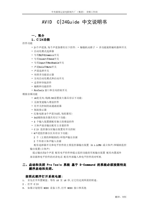
AVID C|24Guide 中文说明书一、简介1、C|24功能控件功能• 24个声道条,每个声道条都有以下控件: • 触敏机动推子 • 多功能旋转编码器和开关• 自动化模式选择器• 专用EQ和Dynamics开关• 专用Insert和Send开关• 专用Input和RecEnable开关• 声道Solo和Mute开关• 声道选择开关• 双排多功能显示器• 全局自动化模式和启动开关• 走带和导航控件• 编辑和功能控件• ProTools窗口和全局控制开关模拟音频功能• 16麦克风/线路/DI前置放大器具有以下功能:• 无级变速输入增益控件• 有开关控制的高通滤波器• 削波指示器• 幻象电源(8个声道分2组,每组都有)• 8x2辅助混音器具有以下功能:• 8 个输入装置都配有独立的增益控件• 立体声混音输出配有主音量控件• C|24 监控器分区输出装置有开关控制• 6声道监控器分区具有以下功能:2 个 (主要的和辅助的)环绕声输出音源2 个外部立体声输入音源配有选择器开关和电平控件的主要监控器输出装置 (5.1、LCRS 或立体声)和辅助监控输出装置(立体声)提示输出的2个声道 配有电平控件和提示监控功能的耳机输出装置 配有内置或外部音源和电平控件的对讲电话 配有外部输入和电平控件的对听机二、启动和关闭 Pro Tools 系统 基于 D-Command 的系统必须按照特定顺序启动和关闭。
按照此顺序打开系统电源:1、 首先打开外置硬盘。
等待 10 至 15 秒,让它们达到所需的转速。
2 、打开 C|243、 如果计划使用 MIDI 设备工作,打开 MIDI 接口和其他MIDI 装置。
4 、打开全部 Pro Tools 音频接口。
5、 打开计算机。
6 、打开监听音箱放大器或有源音箱。
按照此顺序关闭系统:1、 关闭监听音箱放大器或有源音箱。
2 、关闭全部 Pro Tools 音频接口。
3 、关闭计算机。
X24C01FM中文资料

元器件交易网This X24C01 device has been acquired by IC Microsystems from Xicor, Inc.ICmicIC MICROSYSTEMSTM1KX24C01Serial E PROM2128 x 8 BitFEATURESDESCRIPTIONThe X24C01 is a CMOS 1024 bit serial E PROM, internally organized as 128 x 8. The X24C01 features a serial interface and software protocol allowing operation on a simple two wire bus.2•2.7V to 5.5V Power Supply •Low Power CMOS—Active Current Less Than 1 mA —Standby Current Less Than 50 µA •Internally Organized 128 x 8•2 Wire Serial Interface •Four Byte Page Write Mode •Self Timed Write Cycle—Bidirectional Data Transfer ProtocolXicor E PROMs are designed and tested for applications requiring extended endurance. Inherent data2retention is greater than 100 years.—Typical Write Cycle Time of 5 ms•High Reliability—Endurance: 100,000 Cycles —Data Retention: 100 Years •8-Pin Mini-DIP, 8-PIN MSOP, and 8-PIN SOIC PackagesFUNCTIONAL DIAGRAM(8) V CC (4) V SSSTART CYCLEH.V. GENERATION TIMING & CONTROL(5) SDASTART STOPLOGIC CONTROL LOGIC XDECE PROM 32 X 322(6) SCLLOADINCWORD ADDRESS COUNTER R/WYDEC 8 CK PIN DATA REGISTERDOUTDOUT ACK3837 FHD F01© Xicor, 1991 Patents Pending 3837-1.2 7/28/97 T1/C0/D0 SH1Characteristics subject to change without notice元器件交易网X24C01PIN DESCRIPTIONSSerial Clock (SCL) The SCL input is used to clock all data into and out of the device. Serial Data (SDA) SDA is a bidirectional pin used to transfer data into and out of the device. It is an open drain output and may be wire-ORed with any number of open drain or open collector outputs. An open drain output requires the use of a pull-up resistor. For selecting typical values, refer to the Guidelines for Calculating Typical Values of Bus Pull-Up Resistors graph.SOIC/MSOP 1 2 3 4 X24C01 8 7 6 5V CC NCPIN CONFIGURATIONDIP PLASTIC 1 2 3 4 X24C01 8 7 6 5NC NCV CC NCNCV SSSCL SDA3837 FHD F02PIN NAMES Symbol NC VSS VCC SDA SCL A.C. CONDITIONS OF TEST Input Pulse LevelsInput Rise and Fall Times Input and Output Timing LevelsNC NCDescription No Connect Ground Supply Voltage Serial Data Serial Clock3837 PGM T01NCV SSSCL SDA3837 FHD F03EQUIVALENT A.C. LOAD CIRCUIT5V 2190ΟVCC x 0.1 to VCC x 0.910 nsOUTPUTVCC x 0.53837 PGM T02100pF3837 FHD F162元器件交易网X24C01DEVICE OPERATIONThe X24C01 supports a bidirectional bus oriented protocol. The protocol defines any device that sends data onto the bus as a transmitter and the receiving device as the receiver. The device controlling the transfer is a master and the device being controlled is the slave. The master will always initiate data transfers and provide theClock and Data Conventions Data states on the SDA line can change only during SCL LOW. SDA state changes during SCL HIGH are reserved for indicating start and stop conditions. Refer to Figures 1 and 2. Start Condition All commands are preceded by the start condition, which is a HIGH to LOW transition of SDA when SCL is HIGH. The X24C01 continuously monitors the SDA and SCL lines for the start condition and will not respond toclock for both transmit and receive operations. Therefore, the X24C01 will be considered a slave in allapplications.any command until this condition has been met. Figure 1. Data ValiditySCLSDA DATA STABLE DATA CHANGE3837 FHD F063元器件交易网X24C01The X24C01 will respond with an acknowledge after recognition of a start condition, a seven bit word address and a R/W bit. If a write operation has been selected, the X24C01 will respond with an acknowledge after eachStop Condition All communications must be terminated by a stop condition, which is a LOW to HIGH transition of SDA when SCL is HIGH. The stop condition is also used by the X24C01 to place the device in the standby power mode after a read sequence. A stop condition can only be issued after the transmitting device has released the bus. Acknowledge Acknowledge is a software convention used to indicate successful data transfers. The transmitting device will release the bus after transmitting eight bits. During the ninth clock cycle the receiver will pull the SDA line LOWbyte of data is received.In the read mode the X24C01 will transmit eight bits of data, release the SDA line and monitor the line for an acknowledge. If an acknowledge is detected and no stop condition is generated by the master, the X24C01 will continue to transmit data. If an acknowledge is not detected, the X24C01 will terminate further data transmissions. The master must then issue a stop condition to return the X24C01 to the standby power mode andto acknowledge that it received the eight bits of data. Refer to Figure 3.place the device into a known state.Figure 2. Definition of Start and StopSCLSDA START CONDITION STOP CONDITION3837 FHD F07Figure 3. Acknowledge Response From ReceiverSCL FROM MASTER189DATA OUTPUT FROM TRANSMITTERDATA OUTPUT FROM RECEIVERSTARTACKNOWLEDGE3837 FHD F084元器件交易网X24C01WRITE OPERATIONSByte Write To initiate a write operation, the master sends a start condition followed by a seven bit word address and a write bit. The X24C01 responds with an acknowledge, then waits for eight bits of data and then responds with an acknowledge. The master then terminates the transfer by generating a stop condition, at which time the X24C01 begins the internal write cycle to the nonvolatile memory. While the internal write cycle is in progress, the X24C01 inputs are disabled, and the device will not respond to any requests from the master. Refer to Figure 4 for the address, acknowledge and data transfer sequence. Page Write The most significant five bits of the word address define the page address. The X24C01 is capable of a four byte page write operation. It is initiated in the same manner asthe byte write operation, but instead of terminating the transfer of data after the first data byte, the master cantransmit up to three more bytes. After the receipt of each data byte, the X24C01 will respond with an acknowledge. After the receipt of each data byte, the two low order address bits are internally incremented by one. The high order five bits of the address remain constant. If the master should transmit more than four data bytes prior to generating the stop condition, the address counter will “roll over” and the previously transmitted data will be overwritten. As with the byte write operation, all inputs are disabled until completion of the internal write cycle. Refer to Figure 5 for the address, acknowledge and data transfer sequence.Figure 4. Byte WriteS TBUS ACTIVITY:WORD A ADDRESS (n) R T SM SDATA nS TO PSDA LINEBUS ACTIVITY: X24C01PL R A S / C K BBWA C K3837 FHD F09Figure 5. Page WriteS TBUS ACTIVITY:A RWORD ADDRESS (n)DATA nDATA n+1DATA n+3S TO PT SDA LINEBUS ACTIVITY: X24C01SM SPL R A S / C K BA CA CA CBWKKK3837 FHD F105元器件交易网X24C01Figure 6. ACK Polling SequenceWRITE OPERATION COMPLETEDAcknowledge Polling The disabling of the inputs can be used to take advantage of the typical 5 ms write cycle time. Once the stop condition is issued to indicate the end of the host’s write operation the X24C01 initiates the internal write cycle. ACK polling can be initiated immediately. This involves issuing the start condition followed by the word address for a write operation. If the X24C01 is still busy with the write operation no ACK will be returned. If the X24C01 has completed the write operation an ACK will be returned and the controller can then proceed with theENTER ACK POLLINGISSUE STARTnext read or write operation. READ OPERATIONSRead operations are initiated in the same manner as write operations with exception that the R/W bit of theword address is set to a one. There are two basic read operations: byte read and sequential read. It should be noted that the ninth clock cycle of the read operation is not a “don’t care.” To terminate a read operation, the master must either issue a stop condition during the ninth cycle or hold SDA HIGH during the ninthACK RETURNED? ISSUE SLAVE ADDRESS AND R/W = 0ISSUE STOPNOYESNEXT OPERATIONNOclock cycle and then issue a stop condition.Byte Read To initiate a read operation, the master sends a start condition followed by a seven bit word address and aread bit. The X24C01 responds with an acknowledge and then transmits the eight bits of data. The read operation is terminated by the master; by not responding with an acknowledge and by issuing a stop condition.A WRITE? YES ISSUE STOPPROCEEDPROCEED3837 FHD F11Refer to Figure 7 for the start, word address, read bit, acknowledge and data transfer sequence.Figure 7. Byte ReadS TBUS ACTIVITY: MASTERWORD A ADDRESS n RS TO PT SM SSDA LINEBUS ACTIVITY: X24C01PL R A S / C K BBWDATA n3837 FHD F126元器件交易网X24C01Sequential Read Sequential read is initiated in the same manner as the byte read. The first data byte is transmitted as with thebyte read mode, however, the master now responds with an acknowledge, indicating it requires additional data. The X24C01 continues to output data for each acknowledge received. The read operation is terminated by the master; by not responding with an acknowledge and by issuing a stop condition. The data output is sequential, with the data from address n followed by the data from n + 1. The address counter for read operations increments all address bits, allowing the entire memory contents to be serially read during one operation. At the end of the address space (address 127) the counter “rolls over” to zero and the X24C01 continues to output data for each acknowledge received. Refer to Figure 8 for the address, acknowledgeand data transfer sequence.Figure 8. Sequential ReadA C A C A CS TO PBUS ACTIVITY: ADDRESSK SDA LINEBUS ACTIVITY: X24C01KKPA R / CWKDATA nDATA n+1DATA n+2DATA n+x3837 FHD F13Figure 9. Typical System ConfigurationV CCPULL-UP RESISTORS SDA SCL MASTER TRANSMITTER/ SLAVE RECEIVER SLAVE TRANSMITTER/ MASTER TRANSMITTER MASTER TRANSMITTER/RECEIVERRECEIVERRECEIVER3837 FHD F147元器件交易网X24C01ABSOLUTE MAXIMUM RATINGS* Temperature Under Bias .................. –65°C to +135°C *COMMENT Stresses above those listed under “Absolute Maximum Ratings” may cause permanent damage to the device. This is a stress rating only and the functional operation of the device at these or any other conditions above thoseindicated in the operational sections of this specification is not implied. Exposure to absolute maximum rating conditionsStorage Temperature ....................... –65°C to +150°C Voltage on any Pin with Respect to VSS ............................ –1.0V to +7.0V D.C. Output Current ............................................ 5 mA Lead Temperature (Soldering, ............................. 300°C 10 Seconds) RECOMMENDED OPERATING CONDITIONS Temperature Commercial Industrial Military Min. 0°C –40°C –55°C Max. 70°C +85°C +125°Cfor extended periods may affect device reliability.Supply Voltage X24C01 X24C01-3.5 X24C01-3 X24C01-2.7Limits 4.5V to 5.5V 3.5V to 5.5V 3.0V to 5.5V 2.7V to 5.5VD.C. OPERATING CHARACTERISTICS (Over recommended operating conditions, unless otherwise specified)Limits Symbol I ICC(2) ISB1(1)(1) CCParameter VCC Supply Current (Read) VCC Supply Current (Write) VCC Standby Current VCC Standby Current Input Leakage Current Output Leakage Current Input Low Voltage Input High Voltage Output Low VoltageMin.Max. 1 2 100Units mA ∝A ∝A ∝A ∝A V V VTest Conditions SCL = VCC x 0.1/VCC x 0.9 Levels @ 100 KHz, SDA = OpenSCL = SDA = VCC, VCC = 5V ± 10%ISB2(1) ILI ILO VlL(2) VIH(2) VOL50 10 10 VCC x 0.3 –1.0 VCC x 0.7VCC + 0.5 0.4SCL = SDA = VCC, VCC = 2.7VVIN = GND to VCC VOUT = GND to VCCIOL = 2.1 mA3837 PGM T03CAPACITANCE TA = 25°C, f = 1.0 MHz, VCC = 5VSymbol CI/O(3) CIN(3)Parameter Input/Output Capacitance (SDA) Input Capacitance (SCL)Max. 8 6Units pF pFTest Conditions VI/O = 0V VIN = 0V3837 PGM T05Notes: (1) Must perform a stop command prior to measurement. (2) VIL min. and VIH max. are for reference only and are not tested. (3) This parameter is periodically sampled and not 100% tested.8元器件交易网X24C01A.C. CHARACTERISTICS (Over recommended operating conditions, unless otherwise specified)Read & Write Cycle Limits Symbol fSCL TI tAA tBUF tHD:STA tLOW tHIGH tSU:STA tHD:DAT tSU:DAT tR tF tSU:STO tDH POWER-UP TIMING Symbol tPUR(4) tPUW(4) Bus TimingtParameter SCL Clock Frequency Noise Suppression Time Constant at SCL, SDA Inputs SCL Low to SDA Data Out Valid Time the Bus Must Be Free Before a New Transmission Can Start Start Condition Hold Time Clock Low Period Clock High Period Start Condition Setup Time Data In Hold Time Data In Setup Time SDA and SCL Rise Time SDA and SCL Fall Time Stop Condition Setup Time Data Out Hold TimeMin. 0Max. 100 100 3.5Units KHz ns ∝s ∝s ∝s ∝s ∝s ∝s ∝s0.3 4.7 4.0 4.7 4.0 4.7 0 2501 300 4.7 300ns ∝s ns ∝s ns3837 PGM T06Parameter Power-up to Read Operation Power-up to Write OperationMax. 1 5Units ms ms3837 PGM T07FtHIGHtLOWtRSCLtSU:STAtHD:STAtHD:DATtSU:DATtSU:STOSDA INt t tAADHBUFSDA OUT3837 FHD F04Note:(4) tPUR and tPUW are the delays required from the time VCC is stable until the specified operation can be initiated. These parameters are periodically sampled and not 100% tested.9元器件交易网X24C01WRITE CYCLE LIMITS Symbol tWR(6) Parameter Write Cycle Time Min. Typ. 5(5)Max. 10Units ms3837 PGM T08The write cycle time is the time from a valid stop condition of a write sequence to the end of the internal erase/program cycle. During the write cycle, the X24C01bus interface circuits are disabled, SDA is allowed to remain high, and the device does not respond to its word address.Write Cycle TimingSCLSDA8th BIT WORD nACKtWRSTOP CONDITIONSTART CONDITIONX24C01 ADDRESS3837 FHD F05Notes: (5) Typical values are for TA = 25°C and nominal supply voltage (5V). (6) tWR is the minimum cycle time to be allowed from the system perspective unless polling techniques are used. It is the maximum time the device requires to automatically complete the internal write operation.Guidelines for Calculating Typical Values of Bus Pull-Up ResistorsSYMBOL TABLEWAVEFORM INPUTS Must be steady May change from Low to High May change from High to LowDon’t Care: ChangesOUTPUTS Will be steady Will change from Low to High Will change from High to Low Changing: State Not Known Center Line is High Impedance120 RESISTANCE (KΟ) 100 80 60 40 20 0 0 20 40R MINV=CC MAX I OL MIN t R C BUS=2.6KΟR MAX=MAX. RESISTANCEMIN. RESISTANCE6080100120Allowed N/A3837 FHD F15BUS CAPACITANCE (pF)10元器件交易网X24C01PACKAGING INFORMATION8-LEAD PLASTIC IN-LINE PACKAGE TYPE P0.430 (10.92) 0.360 (9.14)0.092 (2.34) DIA. NOM.0.255 (6.47) 0.245 (6.22)PIN 1 INDEX PIN 10.300 (7.62) REF. 0.060 (1.52) 0.020 (0.51)HALF SHOULDER WIDTH ON ALL END PINS OPTIONALSEATING PLANE0.140 (3.56) 0.130 (3.30)0.150 (3.81) 0.125 (3.18)0.020 (0.51) 0.015 (0.38) 0.062 (1.57) 0.058 (1.47)0.110 (2.79) 0.090 (2.29)0.020 (0.51) 0.016 (0.41)0.015 (0.38) MAX.0.325 (8.25) 0.300 (7.62)TYP. 0.010 (0.25)0° 15°NOTE: ALL DIMENSIONS IN INCHES (IN PARENTHESES IN MILLIMETERS)11元器件交易网X24C01PACKAGING INFORMATION8-LEAD PLASTIC SMALL OUTLINE GULL WING PACKAGE TYPE S0.150 (3.80) 0.158 (4.00)0.228 (5.80) 0.244 (6.20)PIN 1 INDEXPIN 10.014 (0.35) 0.019 (0.49)0.188 (4.78) 0.197 (5.00)(4X) 7°0.053 (1.35) 0.069 (1.75)0.050 (1.27)0.004 (0.19) 0.010 (0.25)0.010 (0.25) X 45° 0.020 (0.50)0° – 8°0.0075 (0.19) 0.010 (0.25)0.027 (0.683) 0.037 (0.937)NOTE: ALL DIMENSIONS IN INCHES (IN PARENTHESIS IN MILLIMETERS)3926 FHD F2212元器件交易网X24C01PACKAGING INFORMATION8-LEAD MINIATURE SMALL OUTLINE GULL WING PACKAGE TYPE M0.118 ± 0.002 (3.00 ± 0.05)0.012 + 0.006 / -0.002 (0.30 + 0.15 / -0.05)0.0256 (0.65) TYPR 0.014 (0.36)0.118 ± 0.002 (3.00 ± 0.05)0.030 (0.76) 0.0216 (0.55)0.036 (0.91) 0.032 (0.81)7° TYP0.040 ± 0.002 (1.02 ± 0.05)0.008 (0.20) 0.004 (0.10)0.007 (0.18) 0.005 (0.13)0.150 (3.81) REF. 0.193 (4.90) REF.NOTE: 1. ALL DIMENSIONS IN INCHES AND (MILLIMETERS)3003 ILL 0113元器件交易网X24C01ORDERING INFORMATIONX24C01 Device P T G -V VCC Limits Blank = 4.5V to 5.5V 3.5 = 3.5V to 5.5V 3 = 3.0V to 5.5V 2.7 = 2.7V to 5.5V G=RoHS Compliant Lead Free package Blank = Standard package. Non lead freeTemperature Range Blank = Commercial = 0°C to +70°C I = Industrial = –40°C to +85°C M = Military = –55°C to +125°C Package P = 8-Lead Plastic DIP S = 8-Lead SOIC M = 8-Lead MSOPPart Mark ConventionX24C01XGXBlank = 8-Lead SOIC P = 8-Lead Plastic DIP M = 8-Lead MSOP G = RoHS compliant lead freeBlank = 4.5V to 5.5V, 0°C to +70°C F = 2.7V to 5.5V, 0°C to +70°C G = 2.7V to 5.5V, –40°C to +85°C I = 4.5V to 5.5V, –40°C to +85°C B = 3.5V to 5.5V, 0°C to +70°C C = 3.5V to 5.5V, –40°C to +85°C D = 3.0V to 5.5V, 0°C to +70°C E = 3.0V to 5.5V, –40°C to +85°C M = 4.5V to 5.5V, –55°C to +125°CLIMITED WARRANTYDevices sold by Xicor, Inc. are covered by the warranty and patent indemnification provisions appearing in its Terms of Sale only. Xicor, Inc. makes no warranty, express, statutory, implied, or by description regarding the information set forth herein or regarding the freedom of the described devices from patent infringement. Xicor, Inc. makes no warranty of merchantability or fitness for any purpose. Xicor, Inc. reserves the right to discontinue production and change specifications and prices at any time and without notice. Xicor, Inc. assumes no responsibility for the use of any circuitry other than circuitry embodied in a Xicor, Inc. product. No other circuits, patents, licenses are implied.U.S. PATENTS Xicor products are covered by one or more of the following U.S. Patents: 4,263,664; 4,274,012; 4,300,212; 4,314,265; 4,326,134; 4,393,481; 4,404,475; 4,450,402; 4,486,769; 4,488,060; 4,520,461; 4,533,846; 4,599,706; 4,617,652; 4,668,932; 4,752,912; 4,829, 482; 4,874, 967; 4,883, 976. Foreign patents and additional patents pending. LIFE RELATED POLICY In situations where semiconductor component failure may endanger life, system designers using this product should design the system with appropriate error detection and correction, redundancy and back-up features to prevent such an occurrence. Xicor's products are not authorized for use in critical components in life support devices or systems. 1. Life support devices or systems are devices or systems which, (a) are intended for surgical implant into the body, or (b) support or sustain life, and whose failure to perform, when properly used in accordance with instructions for use provided in the labeling, can be reasonably expected to result in a significant injury to the user. 2. A critical component is any component of a life support device or system whose failure to perform can be reasonably expected to cause the failure of the life support device or system, or to affect its safety or effectiveness.14。
24c02中文资料

24c02中文资料1. 简介24c02是Microchip公司推出的一种串行电子可擦写可编程读写存储器,属于EEPROM(Electrically Erasable Programmable Read-Only Memory)系列。
它采用2-wire串行总线(I2C)接口,具有体积小、功耗低、可靠性高等特点。
本文档将详细介绍24c02的硬件特性、接口规范、存储容量和使用方法。
2. 硬件特性24c02的主要硬件特性如下:•存储容量:24c02有256个字节,每个字节有8位,总计拥有2Kb的存储空间。
•工作电源:24c02需要使用3.3V到5V的供电电压,支持广泛的电源电压范围。
•通信接口:24c02使用I2C串行总线进行通信,具有两根信号线:串行数据线(SDA)和串行时钟线(SCL)。
•封装类型:24c02有多种封装类型可供选择,如DIP(双列直插式封装)、SOP(小型轻负载封装)等。
3. 接口规范24c02采用I2C串行总线接口,其接口规范如下:•数据传输方式:24c02支持字节读写操作和页写操作。
字节读写操作是指每次读写一个字节的数据;页写操作是指每次可以写入8个连续字节的数据。
•起始信号和停止信号:在I2C总线上进行通信时,需要发送起始信号(Start)和停止信号(Stop)以标识数据传输的开始和结束。
•从器件地址:24c02有多个从器件地址可供选择,通过设置硬件地址引脚,可以实现多个24c02器件的级联。
4. 存储容量24c02的存储容量为2Kb,相当于256个字节。
每个字节有8位,可存储0x00到0xFF的数据。
这些存储空间可以被分为多个页,每页包含8个字节。
5. 使用方法以下是24c02的基本使用方法,供参考:•初始化:将24c02与主控芯片(如单片机)连接,并提供正常的供电电源。
同时,设置24c02的硬件地址引脚,确保能正确寻址。
•写入数据:选择要写入数据的存储地址,发送起始信号和器件地址,然后发送数据字节。
CAT24C321中文资料
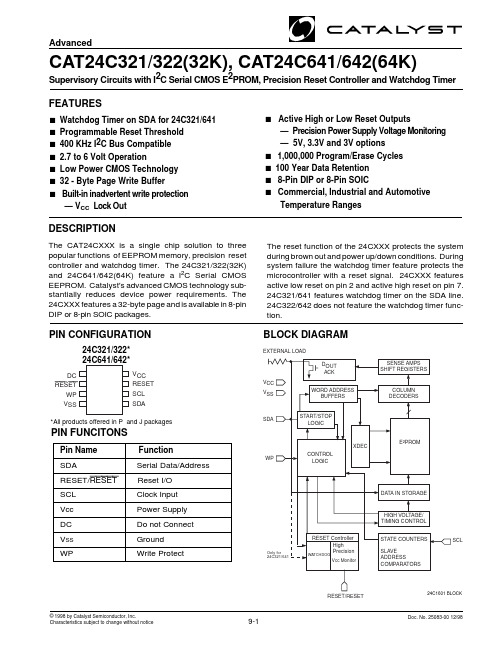
© 1998 by Catalyst Semiconductor, Inc. Characteristics subject to change without noticeDoc. No. 25083-00 12/989-1CAT24C321/322/641/6422AdvancedDoc. No. 25083-00 12/98ABSOLUTE MAXIMUM RATINGS*Temperature Under Bias....................–55°C to +125°C Storage Temperature........................ –65°C to +150°C Voltage on Any Pin withRespect to Ground (1) ..............–2.0V to +V CC + 2.0V V CC with Respect to Ground..................–2.0V to +7.0V Package Power DissipationCapability (Ta = 25°C)1.0W.................................1.0W Lead Soldering Temperature (10 secs)...............300°C Output Short Circuit Current (2) ..........................100mACOMMENTStresses above those listed under “Absolute Maximum Ratings” may cause permanent damage to the device.These are stress ratings only, and functional operation of the device at these or any other conditions outside of those listed in the operational sections of this specifica-tion is not implied. Exposure to any absolute maximum rating for extended periods may affect device perfor-mance and reliability.RELIABILITY CHARACTERISTICSSymbol Parameter Min.Max. Units Reference Test MethodN END (3)Endurance 1,000,000 Cycles/Byte MIL-STD-883, Test Method 1033 T DR (3)Data Retention 100 Years MIL-STD-883, Test Method 1008 V ZAP (3)ESD Susceptibility 2000 Volts MIL-STD-883, Test Method 3015 I LTH (3)(4)Latch-up 100 mAJEDEC Standard 17D.C. OPERATING CHARACTERISTICSV CC = +2.7V to +6.0V, unless otherwise specified.Symbol Parameter Min. Typ. Max. Units Test Conditions I CC Power Supply Current 3mA f SCL = 100 KHzIsbStandby Current40 µAVcc=3.3V50 µA Vcc=5I LI Input Leakage Current 2 µA V IN =G ND or V CC I LO Output Leakage Current10µA V IN =G ND or V CCV IL Input Low Voltage –1 V CC x 0.3 V V IH Input High Voltage V CC x 0.7 V CC + 0.5 VV OLOutput Low Voltage (SDA)0.4 V I OL = 3 mA ,V CC =3.0VLimitsCAPACITANCE T A = 25°C, f = 1.0 MHz, V CC = 5V Symbol Test Max.Units Conditions C I/O (3) Input/Output Capacitance (SDA)8pF V I/O = 0V C IN (3)Input Capacitance (SCL)6pFV IN = 0VNote:(1)The minimum DC input voltage is –0.5V. During transitions, inputs may undershoot to –2.0V for periods of less than 20 ns. Maximum DCvoltage on output pins is V CC +0.5V, which may overshoot to V CC + 2.0V for periods of less than 20ns.(2)Output shorted for no more than one second. No more than one output shorted at a time.(3)This parameter is tested initially and after a design or process change that affects the parameter.(4)Latch-up protection is provided for stresses up to 100 mA on address and data pins from –1V to V CC +1V.CAT24C321/322/641/6423AdvancedDoc. No. 25083-00 12/98A.C. CHARACTERISTICSV CC =2.7V to 6.0V unless otherwise specified.Output Load is 1 TTL Gate and 100pFRead & Write Cycle Limits SymbolParameterV CC =2.7V - 6V V CC =4.5V - 5.5V Min.Max.Min.Max.Units F SCL Clock Frequency100400kHz T I (1)Noise Suppression Time200200ns Constant at SCL, SDA Inputs t AA SCL Low to SDA Data Out 3.51µs and ACK Outt BUF (1)Time the Bus Must be Free Before 4.7 1.2µs a New Transmission Can Start t HD:STA Start Condition Hold Time 40.6µs t LOW Clock Low Period 4.7 1.2µs t HIGH Clock High Period40.6µs t SU:STA Start Condition Setup Time4.70.6µs (for a Repeated Start Condition)t HD:DAT Data In Hold Time 00ns t SU:DAT Data In Setup Time 5050ns t R (1)SDA and SCL Rise Time 10.3µs t F (1)SDA and SCL Fall Time 300300ns t SU:STO Stop Condition Setup Time 40.6µs t DHData Out Hold Time100100nsPower-Up Timing (1)(2)Symbol ParameterMax.Units t PUR Power-up to Read Operation 1ms t PUWPower-up to Write Operation1msNote:(1)This parameter is tested initially and after a design or process change that affects the parameter.(2)t PUR and t PUW are the delays required from the time V CC is stable until the specified operation can be initiated.Write Cycle Limits Symbol Parameter Min.Typ.Max Units t WRWrite Cycle Time10msThe write cycle time is the time from a valid stop condition of a write sequence to the end of the internal program/erase cycle. During the write cycle, the bus interface circuits are disabled, SDA is allowed to remain high, and the device does not respond to its slave address.CAT24C321/322/641/6424AdvancedDoc. No. 25083-00 12/98RESET CIRCUIT CHARACTERISTICSCAT24C321/322/641/6425AdvancedDoc. No. 25083-00 12/98PIN DESCRIPTIONSWP : WRITE PROTECTIf the pin is tied to V CC the entire memory array becomes Write Protected (READ only). When the pin is tied to V SS or left floating normal read/write operations are allowed to the device.SCL : SERIAL CLOCKThe serial clock input clocks all data transferred into or out of the device.RESET/RESET : RESET I/OThese are open drain pins and can be used as reset trigger inputs. By forcing a reset condition on the pins the device will initiate and maintain a reset condition for approximately 200ms. RESET pin must be connected through a pull-down and RESET pin must be connected through a pull-up device.SDA: SERIAL DATA/ADDRESSThe bidirectional serial data/address pin is used to transfer all data into and out of the device. The SDA pin is an open drain output and can be wire-ORed with other open drain or open collector outputs. In the 24C321/641, the SDA line is also used as the Watchdog Timer Monitor.Reset Controller DescriptionThe CAT24CXXX provides a precision RESET control-ler that ensures correct system operation during brown-out and power-up/down conditions. It is configured with open drain RESET outputs. During power-up, the RESET outputs remain active until V CC reaches the V TH threshold and will continue driving the outputs for approximately 200ms (t PURST ) after reaching V TH. After the t PURST timeout interval, the device will cease to drive reset outputs. At this point the reset outputs will be pulled up or down by their respective pull up/pull down devices. During power-down, the RESET outputs will begin driving active when V CC falls below V TH. The RESET outputs will be valid so long as V CC is >1.0V (V RVALID ).The RESET pins are I/Os; therefore, the CAT24CXXX can act as a signal conditioning circuit for an externally applied reset. The inputs are level triggered; that is, the RESET input in the 24CXXX will initiate a reset timeout after detecting a high and the RESET input in the 24CXXX will initiate a reset timeout after detecting a low.Watchdog TimerThe Watchdog Timer provides an independent protec-tion for microcontrollers. During a system failure, the CAT24C321/641 will respond with a reset signal after a time-out interval of 1.6 seconds for lack of activity.24CXX1 is designed with the Watchdog Timer feature on the SDA input. For the 24C321/641, if the microcontroller does not toggle the SDA input pin within 1.6 seconds the Watchdog Timer times out. This will generate a reset condition on reset outputs. The Watch-dog Timer is cleared by any transition on SDA.As long as the reset signal is asserted, the Watchdog Timer will not count and will stay cleared. 24C322/642does not feature the Watchdog Timer function.DEVICE OPERATIONV CCV RESETCAT24C321/322/641/6426AdvancedDoc. No. 25083-00 12/98Hardware Data ProtectionThe 24CXXX is designed with the following hardware data protection features to provide a high degree of data integrity.(1) The 24CXXX features a WP pin. When WP pin is tied high the entire memory array becomes write protected (read only).(2) The V CC sense provides write protection when V CC falls below the reset threshold value (V TH ). The V CC lock out inhibits writes to the serial EEPROM whenever V CC falls below (power down) V TH or until V CC reaches the reset threshold (power up) V TH .Reset Threshold VoltageFrom the factory the 24CXXX is offered in five different variations of reset threshold voltages. They are 4.50-4.75V, 4.25-4.50V, 3.00-3.15V, 2.85-3.00V and 2.55-2.70V. To provide added flexibility to design engineers using this product, the 24CXXX is designed with an additional feature of programming the reset threshold voltage. This allows the user to change the existing reset threshold voltage to one of the other four reset threshold voltages. Once the reset threshold voltage is selected it will not change even after cycling the power,unless the user uses the programmer to change the reset threshold voltage. However, the programming function is available only through third party programmer manufacturers. Please call Catalyst for a list of program-mer manufacturers who support this function.STOPCONDITIONSTARTCONDITIONADDRESSSCLSDAFigure 3. Write Cycle TimingSTART BITSDASTOP BITSCLFigure 4. Start/Stop TimingSCLSDA INSDA OUTFigure 2. Bus TimingCAT24C321/322/641/6427AdvancedDoc. No. 25083-00 12/98ACKNOWLEDGESTARTSCL FROM MASTERDATA OUTPUTFROM TRANSMITTERDATA OUTPUT FROM RECEIVERFigure 5. Acknowledge TimingFigure 6. Slave Address BitsFUNCTIONAL DESCRIPTIONThe CAT24CXXX supports the I 2C Bus data transmis-sion protocol. This Inter-Integrated Circuit Bus protocol defines any device that sends data to the bus to be a transmitter and any device receiving data to be a re-ceiver. The transfer is controlled by the Master device which generates the serial clock and all START and STOP conditions for bus access. The CAT24CXXX operates as a Slave device. Both the Master device and Slave device can operate as either transmitter or re-ceiver, but the Master device controls which mode is activated.I 2C BUS PROTOCOLThe features of the I 2C bus protocol are defined as follows:(1) Data transfer may be initiated only when the bus is not busy.(2) During a data transfer, the data line must remain stable whenever the clock line is high. Any changes in the data line while the clock line is high will be interpreted as a START or STOP condition.START ConditionThe START Condition precedes all commands to the device, and is defined as a HIGH to LOW transition of SDA when SCL is HIGH. The CAT24CXXX monitors the SDA and SCL lines and will not respond until this condition is met.STOP ConditionA LOW to HIGH transition of SDA when SCL is HIGH determines the STOP condition. All operations must end with a STOP condition.DEVICE ADDRESSINGThe Master begins a transmission by sending a START condition. The Master sends the address of the particu-lar slave device it is requesting. The four most significant bits of the 8-bit slave address are fixed as 1010.The next three bits are don't care. The last bit of the slave address specifies whether a Read or Write operation is to be performed. When this bit is set to 1, a Read operation is selected, and when set to 0, a Write opera-tion is selected.After the Master sends a START condition and the slave address byte, the CAT24CXXX monitors the bus and responds with an acknowledge (on the SDA line) when its address matches the transmitted slave address. The CAT24CXXX then performs a Read or Write operation depending on the state of the R/W bit.1010X R/WX XCAT24C321/322/641/6428AdvancedDoc. No. 25083-00 12/98Figure 7. Byte Write TimingFigure 8. Page Write TimingACKNOWLEDGEAfter a successful data transfer, each receiving device is required to generate an acknowledge. The Acknowledg-ing device pulls down the SDA line during the ninth clock cycle, signaling that it received the 8 bits of data.The CAT24CXXX responds with an acknowledge after receiving a START condition and its slave address. If the device has been selected along with a write operation,it responds with an acknowledge after receiving each 8-bit byte.When the CAT24CXXX begins a READ mode it trans-mits 8 bits of data, releases the SDA line, and monitors the line for an acknowledge. Once it receives this ac-knowledge, the CAT24CXXX will continue to transmit data. If no acknowledge is sent by the Master, the device terminates data transmission and waits for a STOP condition.WRITE OPERATIONSByte WriteIn the Byte Write mode, the Master device sends the START condition and the slave address information (with the R/W bit set to zero) to the Slave device. After t he Slave generates an acknowledge, the Master sends a 8-bit address that is to be written into the address pointers of the CAT24CXXX. After receiving another acknowledge from the Slave, the Master device trans-mits the data to be written into the addressed memory location. The CAT24CXXX acknowledges once more and the Master generates the STOP condition. At this time, the device begins an internal programming cycle to nonvolatile memory. While the cycle is in progress, the device will not respond to any request from the Master device.Page WriteThe 24CXXX writes up to 32 bytes of data in a single write cycle, using the Page Write operation. The page write operation is initiated in the same manner as the byte write operation, however instead of terminating after the initial byte is transmitted, the Master is allowed to send up to 31 additional bytes. After each byte has been transmitted, CAT24CXXX will respond with an acknowledge, and internally increment the lower order address bits by one. The high order bits remain un-changed.If the Master transmits more than 32 bytes before sending the STOP condition, the address counter ‘wraps around’, and previously transmitted data will be overwrit-ten.When all 32 bytes are received, and the STOP condi tion has been sent by the Master, the internal program-ming cycle begins. At this point, all received data is written to the CAT24CXXX in a single write cycle.* = Don't care bit for 24C321/322X= Don't care bitA 15–A 8SLAVE ADDRESSSA C KAC KDATAA C KS T O P P BUS ACTIVITY:MASTERSDA LINES T A R T A 7–A 0BYTE ADDRESS A C K*X X XSLAVE C KC KC KBUS ACTIVITY:MASTERSDA LINES T A BYTE ADDRESS C KS T C K C KC KCAT24C321/322/641/6429AdvancedDoc. No. 25083-00 12/98Figure 9. Immediate Address Read TimingAcknowledge PollingDisabling of the inputs can be used to take advantage of the typical write cycle time. Once the stop condition is issued to indicate the end of the host’s write operation,CAT24CXXX initiates the internal write cycle. ACK poll-ing can be initiated immediately. This involves issuing the start condition followed by the slave address for a write operation. If CAT24CXXX is still busy with the write operation, no ACK will be returned. If CAT24CXXX has completed the write operation, an ACK will be returned and the host can then proceed with the next read or write operation.WRITE PROTECTIONThe Write Protection feature allows the user to protect against inadvertent programming of the memory array.If the WP pin is tied to V CC , the entire memory array is protected and becomes read only. The CAT24CXXX will accept both slave and byte addresses, but the memory location accessed is protected from program-ming by the device's failure to send an acknowledge after the first byte of data is received.READ OPERATIONSThe READ operation for the CAT24CXXX is initiated in the same manner as the write operation with one excep-tion, that R/W bit is set to one. Three different READ operations are possible: Immediate/Current Address READ, Selective/Random READ and Sequential READ.SCL SDA 8TH BIT STOPNO ACKDATA OUT89SLAVE ADDRESSSA C KBUS ACTIVITY:MASTERSDA LINES T A R T N O A C KDATAS T O P PCAT24C321/322/641/64210AdvancedDoc. No. 25083-00 12/98Figure 10. Selective Read TimingFigure 11. Sequential Read TimingImmediate/Current Address ReadThe CAT24CXXX’s address counter contains the ad-dress of the last byte accessed, incremented by one. In other words, if the last READ or WRITE access was to address N, the READ immediately following would ac-cess data from address N+1. If N=E (where E=4095 for 24C321/322 and E=8191 for 24C641/642), then the counter will ‘wrap around’ to address 0 and continue to clock out data. After the CAT24CXXX receives its slave address information (with the R/W bit set to one), it issues an acknowledge, then transmits the 8-bit byte requested. The master device does not send an ac-knowledge, but will generate a STOP condition.Selective/Random ReadSelective/Random READ operations allow the Master device to select at random any memory location for a READ operation. The Master device first performs a ‘dummy’ write operation by sending the START condi-tion, slave address and byte addresses of the location it wishes to read. After CAT24CXXX acknowledges, the Master device sends the START condition and the slave address again, this time with the R/W bit set to one.The CAT24CXXX then responds with its acknowledge and sends the 8-bit byte requested. The master deviceSequential ReadThe Sequential READ operation can be initiated by either the Immediate Address READ or Selective READ operations. After the CAT24CXXX sends the initial 8-bit byte requested, the Master will respond with an acknowledge which tells the device it requires more data. The CAT24CXXX will continue to output an 8-bit byte for each acknowledge sent by the Master. The operation will terminate when the Master fails to respond with an acknowledge, thus sending the STOP condition.The data being transmitted from CAT24CXXX is output-ted sequentially with data from address N followed by data from address N+1. The READ operation address counter increments all of the CAT24CXXX address bits so that the entire memory array can be read during one operation. If more than E (where E= 4095 for 24C321/322, E=511 and E=8191 for 24C641/642) bytes are read out, the counter will ‘wrap around’ and continue to clock out data bytes.does not send an acknowledge but will generate a STOP condition.BUS ACTIVITY:MASTERSDA LINEDATA n+xDATA nC KC KDATA n+1C KS T O O A C KDATA n+2C KSLAVE ADDRESS* = Don't care bit for 24C321/322X= Don't care bitA 15–A 8SLAVE ADDRESSSA C KA C KA C KBUS ACTIVITY:MASTERSDA LINES T A R T A 7–A 0BYTE ADDRESS SLAVEADDRESSSA C KN O A C KS T A R T DATAPS T O P X X X *CAT24C321/322/641/64211Advanced Doc. No. 25083-00 12/98Ordering InformationNote:(1) The device used in the above example is a CAT24C322JI-30TE13 (32K I 2C Memory, SOIC, Industrial Temperature, 3.0-3.15V ResetThreshold Voltage, Tape and Reel)CAT24C321/322/641/64212AdvancedDoc. No. 25083-00 12/98。
24C01中文资料
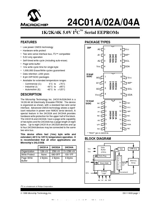
©1996 Microchip Technology Inc.DS11183D-page 124C01A/02A/04AFEATURES•Low power CMOS technology •Hardware write protect•Two wire serial interface bus, I 2 C ™ compatible • 5.0V only operation•Self-timed write cycle (including auto-erase)•Page-write buffer•1ms write cycle time for single byte•1,000,000 Erase/Write cycles guaranteed •Data retention >200 years •8-pin DIP/SOIC packages•Available for extended temperature ranges DESCRIPTIONThe Microchip Technology Inc. 24C01A/02A/04A is a 1K/2K/4K bit Electrically Erasable PROM. The device is organized as shown, with a standard two wire serial interface. Advanced CMOS technology allows a signif-icant reduction in power over NMOS serial devices. A special feature in the 24C02A and 24C04A provides hardware write protection for the upper half of the block.The 24C01A and 24C02A have a page write capability of two bytes and the 24C04A has a page length of eight bytes. Up to eight 24C01A or 24C02A devices and up to four 24C04A devices may be connected to the same two wire bus.This device offers fast (1ms) byte write and extended (-40 ° C to 125 ° C) temperature operation. It is recommended that all other applications use Microchip’s 24LCXXB.-Commercial (C):0˚C to +70˚C -Industrial (I):-40˚C to +85˚C -Automotive (E):-40˚C to +125˚C24C01A24C02A 24C04A Organization 128 x 8258 x 8 2 x 256 x 8Write Protect None 080-0FF 100-1FF Page Write Buffer2 Bytes2 Bytes8 BytesPACKAGE TYPESBLOCK DIAGRAMNC SS CC A0A1NC A2NCV 1234567141312NC SCL SDA NC981110WP V NC * “TEST” pin in 24C01A24C01A 24C02A 24C04A24C01A 24C02A 24C04A24C01A 24C02A 24C04AA0A1A2V SS12348765V CC WP*SCL SDAA0A1A2V SS12348765V CC WP*SCL SDADIP8-leadSOIC14-lead SOICVcc VssSDASCLData Buffer (FIFO)Data Reg.VppR/W AmpMemory ArrayA d d r e s s P o in te rA0 to A7IncrementA8Slave Addr.Control LogicA0A1A2WP1K/2K/4K 5.0V I 2 C ™Serial EEPROMsI 2 C is a trademark of Philips Corporation.This document was created with FrameMaker 404元器件交易网24C01A/02A/04ADS11183D-page 2 © 1996 Microchip Technology Inc.1.0ELECTRICAL CHARACTERISTICS1.1Maximum Ratings*V CC ...................................................................................7.0V All inputs and outputs w.r.t. V SS ...............-0.6V to V CC +1.0V Storage temperature.....................................-65˚C to +150˚C Ambient temp. with power applied................-65˚C to +125˚C Soldering temperature of leads (10 seconds).............+300˚C ESD protection on all pins................................................4 kV*Notice: Stresses above those listed under “Maximum ratings”may cause permanent damage to the device. This is a stress rat-ing only and functional operation of the device at those or any other conditions above those indicated in the operational listings of this specification is not implied. Exposure to maximum rating conditions for extended periods may affect device reliability.TABLE 1-1:PIN FUNCTION TABLEName FunctionA0No Function for 24C04A only, Must be connected to V CC or V SS A0, A1, A2Chip Address Inputs V SS GroundSDA Serial Address/Data I/O SCL Serial ClockTEST (24C01A only) V CC or V SS WP Write Protect Input VCC+5V Power SupplyTABLE 1-2:DC CHARACTERISTICSFIGURE 1-1:BUS TIMING START/STOPVCC = +5V ( ± 10%)Commercial (C):Tamb =0 ° C to +70 ° C Industrial (I):Tamb =-40 ° C to +85 ° C Automotive (E):Tamb =-40 ° C to +125 ° CParameterSymbolMin.Max.Units ConditionsV CC detector threshold V TH 2.8 4.5V SCL and SDA pins:High level input voltage Low level input voltage Low level output voltage V IH V IL V OL V CC x 0.7-0.3V CC + 1V CC x 0.30.4V V V I OL = 3.2 mA (SDA only)A1 & A2 pins:High level input voltage Low level input voltage V IH V IL V CC - 0.5-0.3V CC + 0.50.5V V Input leakage current ILI—10 µ A V IN = 0V to V CC Output leakage current ILO —10 µ A V OUT = 0V to V CCPin capacitance (all inputs/outputs)C IN , C OUT —7.0pF V IN /V OUT = 0V (Note) Tamb = +25˚C, f = 1 MHzOperating current I CC Write — 3.5mA F CLK = 100 kHz, program cycle time = 1 ms, Vcc = 5V, Tamb = 0˚C to +70˚CI CC Write—4.25mAF CLK = 100 kHz, program cycle time = 1 ms, Vcc = 5V, Tamb = (I) and (E)ICC Read—750 µ AV CC = 5V, Tamb= (C), (I) and (E)Standby current ICCS—100 µ A SDA=SCL=VCC=5V (no PROGRAM active)Note:This parameter is periodically sampled and not 100% testedT SU :STAT HD :STAV HYST SU :STOSTART STOPSCLSDA元器件交易网©1996 Microchip Technology Inc.DS11183D-page 324C01A/02A/04ATABLE 1-3:AC CHARACTERISTICSFIGURE 1-2:BUS TIMING DATAParameterSymbol Min.Typ Max.Units RemarksClock frequency F CLK ——100kHz Clock high time T HIGH 4000——ns Clock low timeT LOW 4700——ns SDA and SCL rise time T R ——1000ns SDA and SCL fall time T F ——300ns START condition hold time T HD :S TA 4000——ns After this period the first clock pulse is generated START condition setup time T SU :S TA 4700——ns Only relevant for repeated START conditionData input hold time T HD :D AT 0——ns Data input setup time T SU :D AT 250——nsData output delay time T AA 300—3500(Note 1)STOP condition setup time T SU :S TO 4700——ns Bus free timeT BUF4700——nsTime the bus must be free before a new transmission can startInput filter time constant (SDA and SCL pins)T I ——100ns Program cycle timeTWC—.41ms Byte mode.4N N ms Page mode, N=# of bytesEndurance —1M ——cycles25 °C, Vcc = 5.0V, BlockMode (Note 2)Note 1:As transmitter the device must provide this internal minimum delay time to bridge the undefined region (min-imum 300 ns) of the falling edge of SCL to avoid unintended generation of START or STOP conditions.2:This parameter is not tested but guaranteed by characterization. For endurance estimates in a specific appli-cation, please consult the Total Endurance Model which can be obtained on our BBS or website.T SU :STAT FT LOWT HIGHT RT HD :DATT SU :DAT T SU :STOT HD :STAT BUFT AAT AAT SPT HD :STASCLSDA INSDA OUT元器件交易网24C01A/02A/04ADS11183D-page 4© 1996 Microchip Technology Inc.2.0FUNCTIONAL DESCRIPTIONThe 24C01A/02A/04A supports a bidirectional two wire bus and data transmission protocol. A device that sends data onto the bus is defined as transmitter, and a device receiving data as receiver. The bus has to be controlled by a master device which generates the serial clock (SCL), controls the bus access, and gener-ates the START and STOP conditions, while the 24C01A/02A/04A works as slave. Both master and slave can operate as transmitter or receiver but the master device determines which mode is activated.Up to eight 24C01/24c02s can be connected to the bus,selected by the A0, A1 and A2 chip address inputs. Up to four 24C04As can be connected to the bus, selected by A1 and A2 chip address inputs. A0 must be tied to V CC or V SS for the 24C04A. Other devices can be con-nected to the bus but require different device codes than the 24C01A/02A/04A (refer to section Slave Address).3.0BUS CHARACTERISTICSThe following bus protocol has been defined:•Data transfer may be initiated only when the bus is not busy.•During data transfer, the data line must remain stable whenever the clock line is HIGH. Changes in the data line while the clock line is HIGH will be interpreted as a START or STOP condition.Accordingly, the following bus conditions have been defined (Figure 3-1).3.1Bus not Busy (A)Both data and clock lines remain HIGH.3.2Start Data Transfer (B)A HIGH to LOW transition of the SDA line while the clock (SCL) is HIGH determines a START condition. All commands must be preceded by a START condition.3.3Stop Data Transfer (C)A LOW to HIGH transition of the SDA line while the clock (SCL) is HIGH determines a STOP condition. All operations must be ended with a STOP condition.3.4Data Valid (D)The state of the data line represents valid data when,after a START condition, the data line is stable for the duration of the HIGH period of the clock signal.The data on the line must be changed during the LOW period of the clock signal. There is one clock pulse per bit of data.Each data transfer is initiated with a START condition and terminated with a STOP condition. The number of the data bytes transferred between the START and STOP conditions is determined by the master device and is theoretically unlimited.3.5AcknowledgeEach receiving device, when addressed, is obliged to generate an acknowledge after the reception of each byte. The master device must generate an extra clock pulse which is associated with this acknowledge bit.The device that acknowledges has to pull down the SDA line during the acknowledge clock pulse in such a way that the SDA line is stable LOW during the HIGH period of the acknowledge related clock pulse. Of course, setup and hold times must be taken into account. A master must signal an end of data to the slave by not generating an acknowledge bit on the last byte that has been clocked out of the slave. In this case, the slave must leave the data line HIGH to enable the master to generate the STOP condition.Note:The 24C01A/02A/04A does not generate any acknowledge bits if an internal pro-gramming cycle is in progress.FIGURE 3-1:DATA TRANSFER SEQUENCE ON THE SERIAL BUS(A)(B)(D)(D)(A)(C)START CONDITIONADDRESS OR ACKNOWLEDGEVALID DATA ALLOWED TO CHANGESTOP CONDITIONSCLSDA元器件交易网© 1996 Microchip Technology Inc.DS11183D-page 524C01A/02A/04A4.0SLAVE ADDRESSThe chip address inputs A0, A1 and A2 of each 24C01A/02A/04A must be externally connected to either V CC or ground (V SS ), assigning to each 24C01A/02A/04A a unique address. A0 is not used on the 24C04A and must be connected to either V CC or V SS . Up to eight 24C01A or 24C02A devices and up to four 24C04A devices may be connected to the bus. Chip selection is then accomplished through software by setting the bits A0, A1 and A2 of the slave address to the corresponding hard-wired logic levels of the selected 24C01A/02A/04A.After generating a START condition, the bus master transmits the slave address consisting of a 4-bit device code (1010) for the 24C01A/02A/04A, followed by the chip address bits A0, A1 and A2. In the 24C04A, the seventh bit of that byte (A0) is used to select the upper block (addresses 100—1FF) or the lower block (addresses 000—0FF) of the array.The eighth bit of slave address determines if the master device wants to read or write to the 24C01A/02A/04A (Figure 4-1).The 24C01A/02A/04A monitors the bus for its corre-sponding slave address all the time. It generates an acknowledge bit if the slave address was true and it is not in a programming mode.FIGURE 4-1:SLAVE ADDRESS ALLOCATION5.0BYTE PROGRAM MODEIn this mode, the master sends addresses and one data byte to the 24C01A/02A/04A.Following the START signal from the master, the device code (4-bits), the slave address (3-bits), and the R/W bit, which is logic LOW, are placed onto the bus by the master. This indicates to the addressed 24C01A/02A/04A that a byte with a word address will follow after it has generated an acknowledge bit. Therefore the next byte transmitted by the master is the word address and will be written into the address pointer of the 24C01A/02A/04A. After receiving the acknowledge of the 24C01A/02A/04A, the master device transmits the data word to be written into the addressed memory location.The 24C01A/02A/04A acknowledges again and the master generates a STOP condition. This initiates the internal programming cycle of the 24C01A/02A/04A (Figure 6-1).SLAVE ADDRESS1010A2A1A0R/W ASTARTREAD/WRITE6.0PAGE PROGRAM MODETo program the 24C01A/02A/04A, the master sends addresses and data to the 24C01A/02A/04A which is the slave (Figure 6-1 and Figure 6-2). This is done by supplying a START condition followed by the 4-bit device code, the 3-bit slave address, and the R/W bit which is defined as a logic LOW for a write. This indi-cates to the addressed slave that a word address will follow so the slave outputs the acknowledge pulse to the master during the ninth clock pulse. When the word address is received by the 24C01A/02A/04A, it places it in the lower 8 bits of the address pointer defining which memory location is to be written. (The A0 bit transmitted with the slave address is the ninth bit of the address pointer for the 24C04A). The 24C01A/02A/04A will generate an acknowledge after every 8-bits received and store them consecutively in a RAM buffer until a STOP condition is detected. This STOP condi-tion initiates the internal programming cycle. The RAM buffer is 2 bytes for the 24C01A/02A and 8 bytes for the 24C04A. If more than 2 bytes are transmitted by the master to the 24C01A/02A, the device will not acknowl-edge the data transfer and the sequence will be aborted. If more than 8 bytes are transmitted by the master to the 24C04A, it will roll over and overwrite the data beginning with the first received byte. This does not affect erase/write cycles of the EEPROM array and is accomplished as a result of only allowing the address registers bottom 3 bits to increment while the upper 5bits remain unchanged.If the master generates a STOP condition after trans-mitting the first data word (Point ‘P’ on Figure 6-1), byte programming mode is entered.The internal, completely self-timed PROGRAM cycle starts after the STOP condition has been generated by the master and all received data bytes in the page buffer will be written in a serial manner.The PROGRAM cycle takes N milliseconds, whereby N is the number of received data bytes (N max = 8 for 24C04A, 2 for 24C01A/02A).元器件交易网24C01A/02A/04ADS11183D-page 6© 1996 Microchip Technology Inc.FIGURE 6-1:BYTE WRITEFIGURE 6-2:PAGE WRITESPBUS ACTIVITY MASTER SDA LINE BUS ACTIVITYS T A R TS T O PCONTROL BYTE WORD ADDRESSDATAA C KA C KA C KSPBUS ACTIVITY MASTERSDA LINE BUS ACTIVITYS T A R TCONTROL BYTE WORD ADDRESS (n)DATA n DATA n + 7S T O PA C KA C KA C KA C KA C KDATA n + 17.0ACKNOWLEDGE POLLINGSince the device will not acknowledge during a write cycle, this can be used to determine when the cycle is complete (this feature can be used to maximize bus throughput). Once the stop condition for a write com-mand has been issued from the master, the device ini-tiates the internally timed write cycle. ACK polling can be initiated immediately. This involves the master send-ing a start condition followed by the control byte for a write command (R/W = 0). If the device is still busy with the write cycle, then no ACK will be returned. If the cycle is complete, then the device will return the ACK and the master can then proceed with the next read or write command. See Figure 7-1 for flow diagram.FIGURE 7-1:ACKNOWLEDGE POLLING FLOWSendWrite CommandSend Stop Condition to Initiate Write CycleSend StartSend Control Byte with R/W = 0Did Device Acknowledge (ACK = 0)?Next OperationNOYES元器件交易网© 1996 Microchip Technology Inc.DS11183D-page 724C01A/02A/04A8.0WRITE PROTECTIONProgramming of the upper half of the memory will not take place if the WP pin of the 24C02A or 24C04A is connected to V CC (+5.0V). The device will accept slave and word addresses but if the memory accessed is write protected by the WP pin, the 24C02A/04A will not generate an acknowledge after the first byte of data has been received, and thus the program cycle will not be started when the STOP condition is asserted. Polarity of the WP pin has no effect on the 24C01A.9.0READ MODEThis mode illustrates master device reading data from the 24C01A/02A/04A.As can be seen from Figure 9-2 and Figure 9-3, the master first sets up the slave and word addresses by doing a write. (Note: Although this is a read mode, the address pointer must be written to). During this period the 24C01A/02A/04A generates the necessary acknowledge bits as defined in the appropriate section.The master now generates another START condition and transmits the slave address again, except this time the read/write bit is set into the read mode. After the slave generates the acknowledge bit, it then outputs the data from the addressed location on to the SDA pin,increments the address pointer and, if it receives an acknowledge from the master, will transmit the next consecutive byte. This auto-increment sequence is only aborted when the master sends a STOP condition instead of an acknowledge.Note 1:If the master knows where the addresspointer is, it can begin the read sequence at the current address (Figure 9-1) and save time transmitting the slave and word addresses.Note 2:In all modes, the address pointer will notincrement through a block (256 byte)boundary, but will rotate back to the first location in that block.FIGURE 9-1:CURRENT ADDRESS READFIGURE 9-2:RANDOM READSPBUS ACTIVITY MASTERSDA LINE BUS ACTIVITYS T A R TS T O PCONTROL BYTEDATA nA C KN O A C KSPSBUS ACTIVITY MASTERSDA LINEBUS ACTIVITYS T A R TS T O PCONTROL BYTE A C KWORD ADDRESS (n)CONTROL BYTES T A R TDATA (n)A C KA C KN O A C K元器件交易网24C01A/02A/04ADS11183D-page 8© 1996 Microchip Technology Inc.FIGURE 9-3:SEQUENTIAL READPBUS ACTIVITY MASTER SDA LINE BUS ACTIVITYS T O PCONTROL BYTEA C KN O A C KDATA n DATA n + 1DATA n + 2DATA n + XA C KA C KA C K10.0PIN DESCRIPTION10.1A0, A1, A2 Chip Address InputsThe levels on these inputs are compared with the cor-responding bits in the slave address. The chip is selected if the compare is true. For 24C04 A0 is no function.Up to eight 24C01A/02A's or up to four 24C04A's can be connected to the bus.These inputs must be connected to either V SS or V CC .10.2SDA Serial Address/Data Input/OutputThis is a bidirectional pin used to transfer addresses and data into and data out of the device. It is an open drain terminal, therefore the SDA bus requires a pull-up resistor to V CC (typical 10K Ω).For normal data transfer, SDA is allowed to change only during SCL LOW. Changes during SCL HIGH are reserved for indicating the START and STOP condi-tions.10.3SCL Serial ClockThis input is used to synchronize the data transfer from and to the device.10.4WP Write ProtectionThis pin must be connected to either V CC or V SS for 24C02A or 24C04A. It has no effect on 24C01A.If tied to V CC , PROGRAM operations onto the upper memory block will not be executed. Read operations are possible.If tied to V SS , normal memory operation is enabled (read/write the entire memory).This feature allows the user to assign the upper half of the memory as ROM which can be protected against accidental programming. When write is disabled, slave address and word address will be acknowledged but data will not be acknowledged.Note 1: A “page” is defined as the maximum num-ber of bytes that can be programmed in a single write cycle. The 24C04A page is 8bytes long; the 24C01A/02A page is 2bytes long.Note 2: A “block” is defined as a continuous areaof memory with distinct boundaries. The address pointer can not cross the bound-ary from one block to another. It will how-ever, wrap around from the end of a block to the first location in the same block. The 24C04A has two blocks, 256 bytes each.The 24C01A and 24C02A each have only one block.元器件交易网元器件交易网24C01A/02A/04A NOTES:© 1996 Microchip Technology Inc.DS11183D-page 924C01A/02A/04ADS11183D-page 10© 1996 Microchip Technology Inc.NOTES:元器件交易网24C01A/02A/04A© 1996 Microchip Technology Inc.DS11183D-page 1124C01A/02A/04A Product Identification SystemTo order or to obtain information, e.g., on pricing or delivery, please use the listed part numbers, and refer to the factory or the listed sales offices.Package:P =Plastic DIPSN =Plastic SOIC (150 mil Body), 8-lead SM =Plastic SOIC (207 mil Body), 8-leadSL =Plastic SOIC (150 mil Body), 14-lead, 24C04A onlyTemperature Blank =0°C to +70°CRange:I =-40°C to +85°C E =-40°C to +125°C Device:24C01A 1K I 2C Serial EEPROM24C01AT 1K I 2C Serial EEPROM (Tape and Reel)24C02A 2K I 2C Serial EEPROM24C02AT 2K I 2C Serial EEPROM (Tape and Reel)24C04A 4K I 2C Serial EEPROM24C04AT4K I 2C Serial EEPROM (Tape and Reel)24C01A/02A/04A-/P元器件交易网DS11183D-page 12© 1996 Microchip Technology Inc.Information contained in this publication regarding device applications and the like is intended through suggestion only and may be superseded by updates. No repre-sentation or warranty is given and no liability is assumed by Microchip Technology Incorporated with respect to the accuracy or use of such information, or infringement of patents or other intellectual property rights arising from such use or otherwise. Use of Microchip’s products as critical components in life support systems is not autho-rized except with express written approval by Microchip. No licenses are conveyed, implicitly or otherwise, under any intellectual property rights. The Microchip logo and name are registered trademarks of Microchip Technology Inc. All rights reserved. All other trademarks mentioned herein are the property of their respective companies.W ORLDWIDE S ALES & S ERVICEASIA/PACIFICChinaMicrochip TechnologyUnit 406 of Shanghai Golden Bridge Bldg.2077 Yan’an Road West, Hongiao District Shanghai, Peoples Republic of China Tel: 86 21 6275 5700Fax: 011 86 21 6275 5060 Hong KongMicrochip Technology RM 3801B, Tower Two Metroplaza223 Hing Fong RoadKwai Fong, N.T. Hong KongTel: 852 2 401 1200 Fax: 852 2 401 3431IndiaMicrochip TechnologyNo. 6, Legacy, Convent Road Bangalore 560 025 IndiaTel: 91 80 526 3148 Fax: 91 80 559 9840KoreaMicrochip Technology168-1, Youngbo Bldg. 3 Floor Samsung-Dong, Kangnam-Ku,Seoul, KoreaTel: 82 2 554 7200 Fax: 82 2 558 5934SingaporeMicrochip Technology 200 Middle Road #10-03 Prime Centre Singapore 188980Tel: 65 334 8870 Fax: 65 334 8850Taiwan, R.O.CMicrochip Technology 10F-1C 207Tung Hua North Road Taipei, Taiwan, ROCTel: 886 2 717 7175 Fax: 886 2 545 0139EUROPEUnited KingdomArizona Microchip Technology Ltd.Unit 6, The CourtyardMeadow Bank, Furlong RoadBourne End, Buckinghamshire SL8 5AJ Tel: 44 1628 850303 Fax: 44 1628 850178FranceArizona Microchip Technology SARL Zone Industrielle de la Bonde 2 Rue du Buisson aux Fraises 91300 Massy - FranceTel: 33 1 69 53 63 20 Fax: 33 1 69 30 90 79GermanyArizona Microchip Technology GmbH Gustav-Heinemann-Ring 125D-81739 Muenchen, GermanyTel: 49 89 627 144 0 Fax: 49 89 627 144 44ItalyArizona Microchip Technology SRLCentro Direzionale Colleone Pas Taurus 1Viale Colleoni 120041 Agrate Brianza Milan ItalyTel: 39 39 6899939 Fax: 39 39 689 9883JAPANMicrochip Technology Intl. Inc.Benex S-1 6F3-18-20, Shin Yokohama Kohoku-Ku, Yokohama Kanagawa 222 JapanTel: 81 45 471 6166 Fax: 81 45 471 61229/3/96AMERICASCorporate OfficeMicrochip Technology Inc.2355 West Chandler Blvd.Chandler, AZ 85224-6199Tel: 602 786-7200 Fax: 602 786-7277Technical Support: 602 786-7627Web: AtlantaMicrochip Technology Inc.500 Sugar Mill Road, Suite 200B Atlanta, GA 30350Tel: 770 640-0034 Fax: 770 640-0307BostonMicrochip Technology Inc.5 Mount Royal Avenue Marlborough, MA 01752Tel: 508 480-9990 Fax: 508 480-8575ChicagoMicrochip Technology Inc.333 Pierce Road, Suite 180Itasca, IL 60143Tel: 708 285-0071 Fax: 708 285-0075DallasMicrochip Technology Inc.14651 Dallas Parkway, Suite 816Dallas, TX 75240-8809Tel: 972 991-7177 Fax: 972 991-8588DaytonMicrochip Technology Inc.Suite 150Two Prestige Place Miamisburg, OH 45342Tel: 513 291-1654 Fax: 513 291-9175Los AngelesMicrochip Technology Inc.18201 Von Karman, Suite 1090Irvine, CA 92612Tel: 714 263-1888 Fax: 714 263-1338New YorkMicrochip Technmgy Inc.150 Motor Parkway, Suite 416Hauppauge, NY 11788Tel: 516 273-5305 Fax: 516 273-5335San JoseMicrochip Technology Inc.2107 North First Street, Suite 590San Jose, CA 95131Tel: 408 436-7950 Fax: 408 436-7955TorontoMicrochip Technology Inc.5925 Airport Road, Suite 200Mississauga, Ontario L4V 1W1, Canada Tel: 905 405-6279Fax: 905 405-6253All rights reserved. © 1996, Microchip Technology Incorporated, USA. 9/96Printed on recycled paper.元器件交易网。
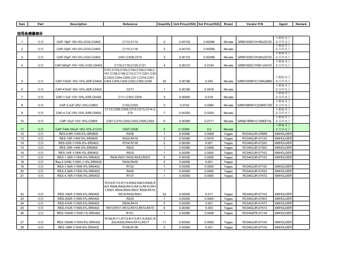
手机成本( 英飞凌+安凯)
Item Part Description Reference Quantity Unit Price(USD)Set Price(USD)Brand Vendor P/N Agent Remark1电容CAP-18pF-16V-5%-COG-C0402C113,C11420.001330.00266Murata GRM1555C1H180JZ01D 1.湘海电子2.首科电子2电容CAP-32pF-16V-5%-COG-C0402C115,C11620.001330.00266Murata 1.湘海电子2.首科电子3电容CAP-33pF-16V-5%-COG-C0402C401,C509,C51030.001330.00399Murata GRM1555C1H330JZ01D 1.湘海电子2.首科电子4电容CAP-560pF-16V-10%-COG-C0402C118,C119,C120,C12140.003100.0124Murata GRM1555C1H561JA01D 1.湘海电子2.首科电子5电容CAP-100nF-16V-10%-X5R-C0402C101,C102,C103,C104,C105,C106,C107,C108,C109,C110,C117,C201,C202,C203,C204,C205,C211,C216,C301,C404,C405,C425,C502,C505,C506250.001800.045Murata GRM155R61C104KA88D1.湘海电子2.首科电子6电容CAP-470nF-16V-10%-X5R-C0402C21710.001800.0018Murata 1.湘海电子2.首科电子7电容CAP-1.0uF-10V-10%-X5R-C0402C111,C501,C50430.006000.018Murata 1.湘海电子2.首科电子8电容CAP-2.2uF-25V-10%-C0603C122,C30320.01420.0284Murata GRM188R61C225KE15D 1.湘海电子2.首科电子9电容CAP-4.7uF-16V-10%-X5R-C0603C112,C206,C209,C212,C213,C214,C21570.003200.0224Murata1.湘海电子2.首科电子10电容CAP-10uF-10V-10%-C0805C207,C210,C302,C403,C406,C50360.002850.0171Murata GRM21BR61C106KE15L 1.湘海电子2.首科电子11电容CAP-TAN-100uF-16V-10%-C1210C507,C50820.100000.2Murata 1.湘海电子2.首科电子12电阻RES-6.8R-1/4W-5%-SR0805R30610.000800.0008Yageo RC0402JR-076R8XMHOLDER 13电阻RES-12R-1/4W-5%-SR0805R302,R41620.000800.0016Yageo RC0402JR-07120XMHOLDER 14电阻RES-22R-1/16W-5%-SR0402R104,R10520.000500.001Yageo RC0402JR-07220XMHOLDER 15电阻RES-30R-1/4W-5%-SR0805R50210.000800.0008Yageo RC0402JR-07300XMHOLDER 16电阻RES-1kR-1/16W-5%-SR0402R50310.000500.0005Yageo RC0402JR-07102XMHOLDER 17电阻RES-1.2kR-1/16W-5%-SR0402R430,R431,R432,R433,R50350.000500.0025Yageo RC0402JR-07122XMHOLDER 18电阻Res,0 OHM,1/16W,+/-5%,SR0402R434,R43520.000500.001Yageo19电阻RES-1.5kR-1/16W-5%-SR0402R10210.000500.0005Yageo RC0402JR-07152XMHOLDER 20电阻RES-2.2kR-1/16W-5%-SR0402R40510.000500.0005Yageo RC0402JR-07222XMHOLDER 21电阻RES-4.7kR-1/16W-5%-SR0402R10710.000500.0005Yageo RC0402JR-07472XMHOLDER22电阻RES-10kR-1/16W-5%-SR0402R103,R110,R114,R402,R403,R406,R407,R408,R409,R410,R412,R415,R417,R501,R504,R505,R507,R508,R516,R519,R520,R301220.000500.011Yageo RC0402JR-07103XMHOLDER23电阻RES-20kR-1/16W-5%-SR0402R20310.000500.0005Yageo RC0402JR-07203XMHOLDER 24电阻RES-47kR-1/16W-5%-SR0402R204,R41420.000500.001Yageo RC0402JR-07473XMHOLDER 25电阻RES-51kR-1/16W-5%-SR0402R510,R511,R512,R513,R514,R51560.000500.003Yageo RC0402JR-07513XMHOLDER 26电阻RES-100kR-1/16W-1%-SR0402R101,10.000800.0008Yageo RC0402FR-07104XMHOLDER27电阻RES-100kR-1/16W-5%-SR0402R106,R111,R112,R113,R115,R201,R202,R205,R404,R413,R517110.000500.0055Yageo RC0402JR-07104XMHOLDER28电阻RES-1MR-1/16W-5%-SR0402R108,R10920.000500.001Yageo RC0402JR-07105XMHOLDER 应用处理器部分29磁珠BLM-75R-25%-300mA-0402L101,L102,L40130.00350.0105Murata BLM15BB750SN11.湘海电子2.首科电子30功率电感IND-3.3uH-10%-1210L20110.0450000.045顺络电子顺络电子31功率电感IND-22uH-10%-1210L30210.0450000.045顺络电子顺络电子32滤波器EXC24CD121FL40110.1083400.1083panasonic33磁珠BLM-600R-25%-100mA-0402B301,B50120.0063030.012606panasonic EXC3BB601H京凌科技34NPN型三极管TRAN-NPN-40V-200mA-SOT23Q401,Q50120.0300000.06Philips PMBT3904,sot23安富利35N沟道增强型MOS管TRAN-MOS-N-60V-TO-236AB Q40210.0300000.03Philips2N7002,sot23安富利36ESD 保护(压敏电阻)RES-VAR-20%-5.5V-0402RD101,D102,D202,D313,D410,D411,D412,D413,D414,D415,D416,D510,D511,D512140.0005000.007Epcos CT0402M4G俊成科技37ESD保护器件RES-6.4Vto7.2V-45pF-SOT23D103,D401,D402,D403,D503,D504,D505,D506,D50790.0340000.306Toshiba DF5A6.8FU台和38二极管DIO-30V-1A-SOD-523/SC-79D201,D412,D418,D50240.0143000.0572Rohm1SS4001.研达科技2.科发电子39肖特基二极管DIO-SCHO-20V-500mA-SOD-123D31710.0143000.0143Diodes B0530WS40键盘灯LED-BLUE-0603-5mA D419,D420,D421,D422,D423,D42460.03000.18佰鸿蓝光LED億威利41SD卡座,CON-SD-Amphenol JS50110.4000000.4Amphenol GSD11001AEU睿吉通电子42触摸屏连接器CON-4pin-0.5SH J10110.0900000.0900Hiros FH19-4S-0.5SH(48)1.信邦电子2.兆崴国际43电池连接器CON-Battery-3pin-2.5PH-4.3H J20110.1000000.1创丰电子BC-3P-2.5PH-4.3H创丰电子44LCD连接器CON-LCD-Nais J30110.2200000.22Nais AXK7L30227G 1.宇科光电2.科通通信45Camera Socket CON-Camera-24pin-Mitsumi J30210.2300000.23Mitsumi R41-8558-A,(M09)1.时毅电子2.时富电子46耳机插座CON-Audio-6pin-Wieson J50110.1500000.15Wieson7272-46,Conn_6Wieson 47尾插CON-Jack-12pin J50210.2300000.23ASTRON060220ASTRON 48侧键CON-SideKey-Cityzen SW423,SW424,SW425,30.08500.255Cityzen LS10时尚科技49处理器IC-AP-AK3223-BGA244U1011 6.1000 6.1Anyka AK3223M Anyka 50反相器IC-Inverter-0.9Vto3.6V-SOT553U10210.10000.1Onsemi553安富利51SDRAM IC-SDRAM-64Mbit-3.0V-x16-TSOP U20110.88000.88Sansung K4M281633H_R(B)N/G/L/F751.AV2.三达52NANDFLASH IC-NAND-512Mb-3.0V-x8-BGA U2021 2.5000 2.5Sansung K9F1208U0B-G,L1.AV2.三达53DC-DC chip DC/DC-POW-1.8V/SOT23-5U20310.35000.35Torex XC9216A18CMRN长天电子54LDO LDO-POW-3V-300mA-SOT-23U20410.25000.25Micrel MIC5259-3.0BD51.世强电讯2.艾睿电子55LDO,3.3V LDO-POW-3.3V-300mA-SOT-23U20510.25000.25Micrel MIC5259-3.3BD51.世强电讯2.艾睿电子56LDO POW-LDO-2.5V-150mA-SOT25U20610.07500.075Torex XC6209A252MR /SOT25长天电子57LCD背光升压芯片POW-DC/DC-2.5Vto6V-SOT23-6U30210.20000.2MPS MP1518TBD58缓冲器IC-Buffer-1.65Vto5.5V-24mA/3V-2.6ns/50pF,5V-MicroPAK U401,U40220.10000.2Fairchild NC7SZ1251.Fairchild2.安富利59晶振CRY-26MHz-10pF-±30ppm-SMD Y10110.20000.2TAITIEN XVCGGCNANF-26MHZ,TAITIEN60晶振CRY-32.768kHz-20pF-±30ppm-SMD Y10210.15000.15Epson MC1461.中电2.众文远达18714.1928561电容CAP-1pF-16V-10%-C0402C70310.002300.0023Murata GRM1555C1H1R0BZ01D 1.湘海电子2.首科电子2电容CAP-1.2pF-16V-10%-C0402C71310.002300.0023Murata GRM1555C1H1R2BZ01D 1.湘海电子2.首科电子3电容CAP-1.8pF-16V-10%-C0402C718,C72220.002800.0056Murata GRM1555C1H1R8BZ01D 1.湘海电子2.首科电子4电容CAP-4.7pF-16V-10%-C0402C72410.002300.0023Murata GRM1555C1H4R7BZ01D 1.湘海电子2.首科电子5电容CAP-18pF-16V-5%-C0402C629,C63020.001330.00266Murata GRM1555C1H180JZ01D 1.湘海电子2.首科电子6电容CAP-27pF-16V-10%-C0402C643,C645,C702,C706,C707,C708,C723,C729,C730,C731,C732110.001330.01463Murata GRM1885C1H270JA01D1.湘海电子2.首科电子7电容CAP-33pF-16V-5%-C0402C631,C632,C63430.001330.00399Murata GRM1555C1H330JZ01D 1.湘海电子2.首科电子8电容CAP-4.7nF-16V-10%-C0402C704,C71720.001300.0026Murata GRM155R71H472KA01D 1.湘海电子2.首科电子9电容CAP-6.8nF-16V-10%-C0402C70110.001300.0013Murata GRM155R71H682KA88D 1.湘海电子2.首科电子10电容CAP-47nF-16V-10%-C0402C601,C705,C70930.002700.0081Murata GRM155R71C473KA01D 1.湘海电子2.首科电子11电容CAP-68nF-16V-10%-C0402C61010.003300.0033Murata GRM155R71C683KA88D 1.湘海电子2.首科电子12电容CAP-100nF-16V-10%-C0402C605,C608,C609,C619,C620,C621,C622,C623,C627,C628,C633,C637,C638,C639,C640,C712160.001580.02528Murata GRM155R71C104KA88D1.湘海电子2.首科电子13电容CAP-2.2uF-16V-10%-C0402C604,C606,C611,C612,C613,C614,C615,C616,C617,C624,C625,C626120.003200.0384Murata1.湘海电子2.首科电子14电容CAP-10uF-16V-10%-C0805C635,C636,C64430.029000.087Murata GRM21BR61C106KE15L 1.湘海电子2.首科电子15电容CAP-22uF-6.3V-20%-TC1210C602,C60720.070000.14Murata GRM31CR60J226ME19L 1.湘海电子2.首科电子16电容CAP-TAN-100uF-6.3V-20%-TC1210C60310.100000.1Murata1.湘海电子2.首科电子17电容CAP-TAN-150uF-6.3V-20%-TC1210C61810.100000.1Murata1.湘海电子2.首科电子18电阻RES-0R-1/16W-5%-SR0402R605,R606,R608,R620,R702,R704,R705,R70670.000500.0035Yageo RC0402JR-070XMHOLDER19电阻RES-0.15R-1/16W-5%-SR0402R60110.030000.03Yageo RC0402JR-070R15XMHOLDER 20电阻RES-4.7R-1/16W-5%-SR0402R60710.000500.0005Yageo RC0402JR-074R7XMHOLDER 21电阻RES-22R-1/16W-5%-SR0402R625,R626,R62730.000500.0015Yageo RC0402JR-07220XMHOLDER 22电阻RES-220R-1/16W-5%-SR0402R701,10.000500.0005Yageo RC0402JR-07221XMHOLDER 23电阻RES-1kR-1/16W-5%-SR0402R703,10.000500.0005Yageo RC0402JR-07102XMHOLDER 24电阻RES-1.5kR-1/16W-5%-SR0402R61810.000500.0005Yageo RC0402JR-07152XMHOLDER 25电阻RES-2.2kR-1/16W-5%-SR0402R62110.000500.0005Yageo RC0402JR-07222XMHOLDER 26电阻RES-4.7kR-1/16W-5%-SR0402R61510.000500.0005Yageo RC0402JR-07472XMHOLDER 27电阻RES-10kR-1/16W-5%-SR0402R61110.000500.0005Yageo RC0402JR-07103XMHOLDER 28电阻RES-22kR-1/16W-5%-SR0402R602,R612,R613,R62240.000500.002Yageo RC0402JR-07223XMHOLDER 29电阻RES-47kR-1/16W-5%-SR0402R61410.000500.0005Yageo RC0402JR-07473XMHOLDER 30电阻RES-82kR-1/16W-5%-SR0402R60910.000810.00081Yageo RC0402JR-07823XMHOLDER 基带射频部分31电阻RES-100kR-1/16W-5%-SR0402R617,R62420.000500.001Yageo RC0402JR-07104XMHOLDER 32电阻RES-220kR-1/16W-5%-SR0402R604,R62320.000500.001Yageo RC0402JR-07224XMHOLDER 33电阻RES-390kR-1/16W-5%-SR0402R61610.000500.0005Yageo RC0402JR-07394XMHOLDER 34电阻RES-560kR-1/16W-5%-SR0402R60310.000500.0005Yageo RC0402JR-07564XMHOLDER 35电阻RES-1MR-1/16W-5%-SR0402R61010.000500.0005Yageo RC0402JR-07105XMHOLDER 36电感IND-1.5nH-10%-0402L70710.00500.005顺络电子顺络电子37电感IND-2.2nH-10%-0402L704,L70520.00500.01顺络电子顺络电子38电感IND-6.2nH-20%-0402-Wirewound L71110.04500.045顺络电子顺络电子39电感IND-15nH-3%-0402-Wirewound L709,L71020.04500.09顺络电子顺络电子40电感IND-10uH-10%-1210L601,L60220.03500.07顺络电子顺络电子41电感BLM15BB750SN1L629,L63020.00350.007Murata42二极管DIO-SCHO-10V-3A-SOD-323D60110.02900.029Infineon BAT60B,品佳电子43ESD保护器件RES-VAR-20%-5.5V-0402R D602,D60320.00050.001Toshiba ESD,CT0402M4G台和44mos管TRAN-MOSFET-P-2.5V-TSOP6Q60110.1050.105Infineon BSL211SP品佳电子45mos管TRAN-MOSFET-P-2.5V-SOT323Q60210.04680.0468Infineon BSS223PW品佳电子46复合管TRAN-PNP/NPN-SOT363Q60310.2160.216Infineon BCR39PN品佳电子47SIM卡座CON-simcard-0.9H JR60110.12000.12linktek SIMSH-00630-TP00良泽电子48射频连接头CON-RF-Murata J70110.11000.11Murata CRS5001-1003_1,MM8430A湘海电子49声表滤波器SAW-Impedance50Ω(I)/150Ω(O)-925to960MHz/InsertionLoss2.7Db/VSWR2.0/RippleDeviation1.8dB/AmplitudeBalance±1.0dB/PhaseBalance180±10°BP70210.15000.15EPCOS B78371.EPCOS2.俊成科技50声表滤波器SAW-Impedance50Ω(I)/150Ω(O)-1805to1880MHz/InsertionLoss2.5dB/VSWR2.2/RippleDeviation1.5dB/AmplitudeBalance±1.5dB/PhaseBalance180±12°BP70310.17000.17EPCOS B78521.EPCOS2.俊成科技51电源管理芯片PMU-PMB6814-VQFN48-Infineon U6011 1.2 1.2Infineon PMB6814品佳电子52存储器IC-FLA-2.7Vto3.1V-32MbNor-8MbpSRAM-56pin FBGA U6021 2.5000 2.5Spansion S71GL032A801.时尚科技2.威健实业53基带/射频处理器BB/RF-PMB7870-LFBGA233-Infineon U6031 4.8 4.8Infineon PMB7870品佳电子54天线开关Switch-ANT-12pin-TDK U70110.58000.58TDK ASM4518807T-250355射频PAPA-2BAND-GSM850(824to849MHz)/GSM900(880to915MHz)/DSC(1710to1785MHz)/ PSC(1850to1910MHz)-GSM35dB/3.5V-DCS/PCS33dB/3.5V-LFM48P U7021 1.3000 1.3RFMD RF31661.光明电子2.世健56晶振p ppSMD Y60110.15000.15MC MS2V-T1S普荣实业57晶振CRY-26MHz-10pF-±10ppm-SMD Y70110.34000.34Kyocera CX3225YB26000F0FLFZZ普荣实业12112.62987PCB 1.5PCBA28.3227261喇叭直径20mm ,弹片式LS10110.50000.5000Keyrin 2咪头MK40110.25000.2500BSE 3马达弹片胶套电机MOTOR50110.43000.4300韩国永柏4受话器32ohm Receiver LS60110.12000.1200Keyrin 5LCD LCD-2.2''-320x240-MPU 112.000012.0000Truly 6摄像头CAM-1.3M-CMOS 1 5.9000 5.9000Sunny7外壳结构件1 2.2000 2.20008电池1 1.2000 1.20009充电器1 1.0000 1.000010数据线10.80000.800011光盘10.15000.150012耳机10.80000.800013包装件10.50000.500025.850054.17271闪光灯驱动U30110.4800000.4800002闪光灯D31110.3800000.380000装配件与周转件可选件整机BOM 20-8E-09Keyrin OBG415L44C1033R宝星电子YB43DD-1麒麟通讯KR -1406C -01PKeyrin Truly 8108H 邦 泽 科 技LM2753SDCL-690S-2WF ,Flash Led。
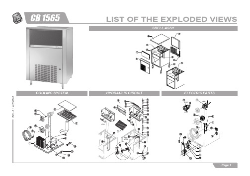
迪杰尔冷却系统外壳组件清单说明书
10 Tensione
Common Parts Ref.
1 Pump 3 Hot Gas Coil 4 Hot Gas Valve Body 7 Contactor 9 Bin Thermostat 10 Evaporator Thermostat 11 Timer 12 Green Light Switch
Rev. 3 - 2/7/2003
Ref. 1 - Ice Cubes Slide Kind of Cube Code
18 g. (Standard) 33 g. (Big) 13 g. (Small)
D12022 D12033 D12040
Ref. 6 - Sprayers Bar Ass.
Kind of Cube
ELECTRIC PARTS
Spare Description See Table
See Table
Code
23091 20409 23594 23005 23591
23327
Parts for Air-Cooled Version Only Ref.
2 Fan Motor 6 Inlet Watervalve 1 Way 8 Condenser Pressure Switch 13 Anti Radio Interference Filter
See Table See Table
Version 2 Version 2 Version 2 Version 2 Version 1 Version 1
Code
10005 C22134
D20002 10012 10305 10133 20233 10241 13006 10055 13007 10096 C13110 10007 10009 C13036 20005 10405 13142 10404 13143 13096 13095
- 1、下载文档前请自行甄别文档内容的完整性,平台不提供额外的编辑、内容补充、找答案等附加服务。
- 2、"仅部分预览"的文档,不可在线预览部分如存在完整性等问题,可反馈申请退款(可完整预览的文档不适用该条件!)。
- 3、如文档侵犯您的权益,请联系客服反馈,我们会尽快为您处理(人工客服工作时间:9:00-18:30)。
n Featuresl Effective in noise suppression of portable equipment l Magnetic shield typel Small size(L 1.25 mm ´W 1.00 mm ´H 0.50 mm) and light weight(About 3 mg)Common mode Noise FiltersType:EXC24CDn Explanation of Part Numbersn Recommended Applicationsl Digital audio and Video equipment such as PDA,DSC, DVC, CD Player, DVD Player, MD Player.l USB data line of Mobile phone (IMT2000).l Small digital equipment such as Personal computers.-1:2+34"5+6,7'891071112Noise FilterHigh speed Differential transmission DCoupled typeThe first two digits are significant figure ofimpedance value,and thethird one denotes the number of zero followingPacking Embossed Carrier Taping Code U Product CodeType Characteristics SizeNominal ImpedanceFormSuffixCNumber of Terminals4Terminals Dimensions(mm)1.25´1.00´0.50(L)´(W)´(H)Code 2n Impedance Characteristics (Typical) Measured by HP4291AEmbossed Carrier Dimensions (mm)Part Number A B W F E P1P2P0f D0t1t2 EXC24CD111U 1.20±0.15 1.45±0.158.0±0.2 3.5±0.11.75±0.10 4.0±0.1 2.0±0.1 4.0±0.1 1.5±0.10.25±0.050.90±0.15Standard Reel Dimensions (mm)Part Number f A f B f C f D E W T tEXC24CD111U180.0±3.060.0±1.013.0±0.521.0±0.8 2.0±0.59.0±0.311.4±1.5 1.2±0.2n Recommended Soldering ConditionsRecommendations and precautions are described below.<Repair with hand soldering>l Use a soldering iron with tip temperature 280 ¡C or less. Solder for 3 seconds or less for each termination.Cautions for SafetyThe following are precautions for individual products. Please also refer to the precautions common to CR Combinations, Fuses, and Sensors shown on page EX3 of this catalog.1. When possible, do not mount Common mode Noise Filters (hereafter called the Filters) by flow soldering. It is highly possible that flow soldering may cause bridges between the electrodes.2. Use rosin-based flux or halogen-free flux.3. For cleaning, use an alcohol-based cleaning agent. Before using any other type, consult with our sales person in advance.4. Do not apply a shock to the Filters or pinch them with a hard tool (e.g. pliers and tweezers). Otherwise, their bodies may be chipped, affecting their performance.Excessive mechanical stress may damage the Filters. Handle with care.5. Store the Filters in a location at a temperature from -5 ¡C to +40 ¡C and relative humidity from 40 % to 60 %, where there are no rapid changes in temperature or humidity.6. Use the Filters within half a year after the date of the outgoing inspection indicated on the packages.Caution for Safety (Common precautions for CR Combinations, Fuses, and Sensors)¥When using our products, no matter what sort of equipment they might be used for, be sure to make a written agreement on the specifications with us in advance. The design and specifications in this catalog are subject to change without prior notice.¥Do not use the products beyond the specifications described in this catalog.¥This catalog explains the quality and performance of the products as individual components. Before use, check and evaluate their operations when installed in your products.¥Install the following systems for a failsafe design to ensure safety if these products are to be used in equipment where a defect in these products may cause the loss of human life or other significant damage, such as damage to vehicles (automobile, train, vessel), traffic lights, medical equipment, aerospace equipment, electric heating appliances, combustion/gas equipment, rotating equipment, and disaster/crime prevention equipment.]Systems equipped with a protection circuit and a protection device]Systems equipped with a redundant circuit or other system to prevent an unsafe status in the event of a single fault(1) Precautions for use¥These products are designed and manufactured for general purpose and standard use in general electronic equipment (e.g. AV equipment, home electric appliances, office equipment, information and communication equipment)¥These products are not intended for use in the following special conditions. Before using the products, carefully check the effects on their quality and performance, and determine whether or not they can be used.1. In liquid, such as water, oil, chemicals, or organic solvent2. In direct sunlight, outdoors, or in dust3. In salty air or air with a high concentration of corrosive gas, such as Cl2, H2S, NH3, SO2, or NO24. In an environment where strong static electricity or electromagnetic waves exist5. In an environment where these products cause dew condensation6. Sealing or coating of these products or a printed circuit board on which these products are mounted, withresin or other materials¥ These products generate Joule heat when energized. Carefully position these products so that their heat will not affect the other components.¥ Carefully position these products so that their temperatures will not exceed the category temperature range due to the effects of neighboring heat-generating components. Do not mount or place heat-generating components or inflammables, such as vinyl-coated wires, near these products (except Thermal Cutoffs).¥Note that non-cleaning solder, halogen-based highly active flux, or water-soluble flux may deteriorate the performance or reliability of the products.¥ Carefully select a flux cleaning agent for use after soldering. An unsuitable agent may deteriorate the performance or reliability. In particular, when using water or a water-soluble cleaning agent, be careful not to leave water residues. Otherwise, the insulation performance may be deteriorated.(2) Precautions for storageThe performance of these products, including the solderability, is guaranteed for a year from the date of arrival at your company, provided that they remain packed as they were when delivered and stored at a temperature of 5 ¡C to 35 ¡C and a relative humidity of 45 % to 85 %.The performance of Combinations(EMI Filters) is guaranteed for 6 months or a year from the outgoing inspection date indicated on the packages, provided that they are stored at a temperature of -5 ¡C to +40 ¡C and a relative humidity of 40 % to 60 %. Check the guarantee period in the specifications. The performance of Thermal Cutoffs is guaranteed for a year from the outgoing inspection date indicated on the packages, provided that they are stored at a temperature of -10 ¡C to +40 ¡C and a relative humidity of 30 % to 75 %.Even within the above guarantee periods, do not store these products in the following conditions. Otherwise, their electrical performance and/or solderability may be deteriorated, and the packaging materials (e.g. taping materials) may be deformed or deteriorated, resulting in mounting failures.1. In salty air or in air with a high concentration of corrosive gas, such as Cl2, H2S, NH3, SO2, or NO22. In direct sunlight<Package markings>Package markings include the product number, quantity, and country of origin.In principle, the country of origin should be indicated in English.。