MAX4014EUK-T中文资料
MAX5144EUB中文资料

CS
2
SCLK 3 DIN 4
MAX5141 MAX5143
7 VDD 6 OUT 5 CLR
MAX5142 MAX5144
8 RFB 7 INV 6 OUT
DIN 4 CLR 5
µMAX
µMAX
Ordering Information
PART MAX5141EUA MAX5142EUB MAX5143EUA MAX5144EUB TEMP. RANGE -40°C to +85°C -40°C to +85°C -40°C to +85°C -40°C to +85°C PIN-PACKAGE 8 µMAX 10 µMAX 8 µMAX 10 µMAX INL (LSB) ±1 ±1 ±1 ±1 SUPPLY RANGE (V) 5 5 3 3 OUTPUT SWING Unipolar Bipolar Unipolar Bipolar
SPI and QSPI are trademarks of Motorola, Inc. MICROWIRE is a trademark of National Semiconductor Corp. ________________________________________________________________ Maxim Integrated Products 1
ELECTRICAL CHARACTERISTICS
(VDD = +3V (MAX5143/MAX5144) or +5V (MAX5141/MAX5142), VREF = +2.5V, TA = TMIN to TMAX, CL = 10pF, GND = 0, RL = ∞, unless otherwise noted. Typical values are at TA = +25°C.) PARAMETER SYMBOL CONDITIONS MIN 14 ±0.5 ±0.5 ±0.05 ±10 ±0.1 ROUT (Note 2) RFB/RINV Ratio error BZSTC PSR +2.7V ≤ VDD ≤ +3.3V (MAX5143/MAX5144) +4.5V ≤ VDD ≤ +5.5V (MAX5141/MAX5142) (Note 3) Unipolar mode Bipolar mode 2.0 10 6 15 1 7 0.2 ±0.5 ±1 ±1 VDD 6.2 1 ±0.03 ±20 ±1 ±1 ±2 TYP MAX UNITS Bits LSB LSB LSB ppm/°C LSB ppm/°C kΩ
MAX491EESD+中文资料
Driver Input Voltage (DI).............................-0.5V to (VCC + 0.5V)
Driver Output Voltage (Y, Z; A, B) ..........................-8V to +12.5V
Receiver Input Voltage (A, B).................................-8V to +12.5V
元器件交易网
MAX481E/MAX483E/MAX485E/MAX487E–MAX491E/MAX1487E
±15kV ESD-Protected, Slew-Rate-Limited, Low-Power, RS-485/RS-422 Transceivers
ABSOLUTE MAXIMUM RATINGS
General Description
The MAX481E, MAX483E, MAX485E, MAX487E– MAX491E, and MAX1487E are low-power transceivers for RS-485 and RS-422 communications in harsh environments. Each driver output and receiver input is protected against ±15kV electro-static discharge (ESD) shocks, without latchup. These parts contain one driver and one receiver. The MAX483E, MAX487E, MAX488E, and MAX489E feature reduced slew-rate drivers that minimize EMI and reduce reflections caused by improperly terminated cables, thus allowing error-free data transmission up to 250kbps. The driver slew rates of the MAX481E, MAX485E, MAX490E, MAX491E, and MAX1487E are not limited, allowing them to transmit up to 2.5Mbps.
MAX4173TEUT-T中文资料

Notebook Computers
Portable/Battery-Powered Systems
Smart Battery Packs/Chargers
Cell Phones
Power-Management Systems
General System/Board-Level Current Monitoring
The combination of three gain versions and a userselectable external sense resistor sets the full-scale current reading. This feature offers a high level of integration, resulting in a simple and compact currentsense solution.
+20V/V (MAX4173T) +50V/V (MAX4173F) +100V/V (MAX4173H) ♦ ±0.5% Full-Scale Accuracy ♦ ±0.3mV Input Offset Voltage (MAX4173T) ♦ 420µA Supply Current ♦ Wide 1.7MHz Bandwidth (MAX4173T) ♦ +3V to +28V Operating Supply ♦ Available in Space-Saving SOT23-6 Package
Typical Operating Circuit
0 TO +28V
VSENSE
+3V TO +28V 0.1µF
nRF401中文手册

表 1. nRF401 主要技术特性
*PWR_UP 管脚间歇供电 占空比 2% 周期 200ms
单位
MHZ
KHz dBm dBm kbit/s
V uA mA uA
定购信息
型号
nRF401-IC nRF401-EVKIT
特性
20pin SSOIC Evaluation kit with nRF401 IC
Sensitivity
@400
.BR=20kbit/s,BER<10-3
Bit rate
ZI
Recommended antenna
port differential impedance
Spurious emission
to +85
最小
典型
最大 单位
2.7
3
5.25
V
0
V
11
mA
8
mA
8
uA
10
DBm
名称 tTR tRT tST tSR tVT tVR
最大延时
3ms 1ms 2ms 3ms 4ms 5ms
条件 连续工作
上电
COPYRIGHT ©2001 ALL RIGHTS RESERVED 迅通科技 TEL: (0451)6349363 6332356 4
433MHZ 单片无线收发芯片
功能描述
真正的单片 FSK 收发芯片 非常少的外围元件 无需进行初始化和配置 不需要对数据进行曼彻斯特编码 最高速率 20Kbps 2 个工作频道 宽工作电压范围 低功耗 待机模式
nRF401
应用领域
报警和安全系统 自动测试系统 家庭自动化控制 遥控装置 车辆安全系统 工业控制 无线通信 电信终端
MAX4466EXK中文资料

5-Pin SC70 (derate 2.5mW/°C above +70°C) .............200mW 5-Pin SOT23 (derate 7.1mW/°C above +70°C) ...........571mW
ELECTRICAL CHARACTERISTICS
(VCC = +5V, VCM = 0, VOUT = VCC/2, RL = ∞ to VCC/2, SHDN = GND (MAX4467/MAX4468 only). TA = TMIN to TMAX, unless otherwise noted. Typical values specified at TA = +25°C.) (Note 1)
TOP VIEW
IN+ 1
5 VCC
MAX4465 GND 2 MAX4466
IN- 3
4 OUT
SC70/SOT23 Pin Configurations continued at end of data sheet.
Rail-to-Rail is a registered trademark of Nippon Motorola, Ltd.
Features
o +2.4V to +5.5V Supply Voltage Operation
o Versions with 5nA Complete Shutdown Available (MAX4467/MAX4468)
MAX1722EZK-T中文资料
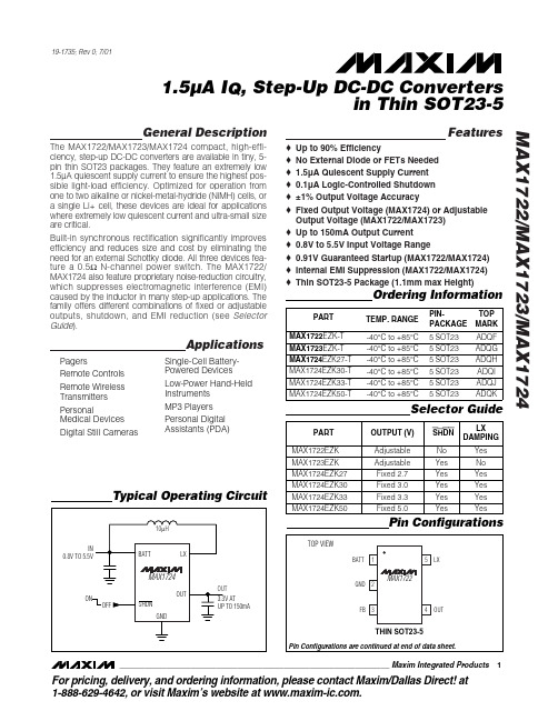
MAX1722
FB 3
4
OUT
THIN SOT23-5
Pin Configurations are continued at end of data sheet.
________________________________________________________________ Maxim Integrated Products
元器件交易网
19-1735; Rev 0; 7/01
1.5µA IQ, Step-Up DC-DC Converters in Thin SOT23-5
General Description
The MAX1722/MAX1723/MAX1724 compact, high-efficiency, step-up DC-DC converters are available in tiny, 5pin thin SOT23 packages. They feature an extremely low 1.5µA quiescent supply current to ensure the highest possible light-load efficiency. Optimized for operation from one to two alkaline or nickel-metal-hydride (NiMH) cells, or a single Li+ cell, these devices are ideal for applications where extremely low quiescent current and ultra-small size are critical. Built-in synchronous rectification significantly improves efficiency and reduces size and cost by eliminating the need for an external Schottky diode. All three devices feature a 0.5Ω N-channel power switch. The MAX1722/ MAX1724 also feature proprietary noise-reduction circuitry, which suppresses electromagnetic interference (EMI) caused by the inductor in many step-up applications. The family offers different combinations of fixed or adjustable outputs, shutdown, and EMI reduction (see Selector Guide). o o o o o o o o o o o
美国Eaton公司产品说明书:Eaton PDG23G0040TFFK电解型防护电路保护器

Eaton PDG23G0040TFFKEaton Power Defense molded case circuit breaker, Globally Rated, Frame 2, Three Pole, 40A, 35kA/480V, T-M (Fxd-Fxd) TU, Standard Terminals Line Only (PDG2X3T100)Eaton Power Defense molded case circuit breakerPDG23G0040TFFK 78667989305088.9 mm 152.4 mm 104.6 mm 1.82 kg Eaton Selling Policy 25-000, one (1) year from the date of installation of theProduct or eighteen (18) months from thedate of shipment of the Product,whichever occurs first.RoHS Compliant IEC 60947-2UL 489CSACCC MarkedProduct NameCatalog Number UPCProduct Length/Depth Product Height Product Width Product Weight WarrantyCompliancesCertifications40 AComplete breaker 2Three-polePD2 Global Class A T-M (Fxd-Fxd) TU600 Vac600 VStandard Terminals Line Only35 kAIC at 480 Vac 25 kAIC Icu/ 20 kAIC Ics/ 52.5 kAIC Icm @480V Brazil (IEC) 35 kAIC @480V (UL) 65 kAIC @240V (UL)30 kAIC Icu/ 22.5 kAIC Ics/ 63 kAIC Icm @440V (IEC) 8 kAIC Icu/ 4 kAIC Ics/ 16.8 kAIC Icm @690V (IEC)20 kAIC Icu/ 15/13 kAIC Ics/ 42 kAIC Icm @525V South Africa (IEC)10 kAIC Icu @250 Vdc36 kAIC Icu/ 36 kAIC Ics/ 75.6 kAIC Icm @380-415V (IEC) 18 kAIC @600V (UL/CSA)55 kAIC Icu/ 55 kAIC Ics/ 121 kAIC Icm @240V (IEC) 10 kAIC Icu @125 VdcEaton Power Defense PDG23G0040TFFK 3D drawing Consulting application guide - molded case circuit breakers Amperage Rating Circuit breaker frame type Frame Number of poles Circuit breaker type Class Trip Type Voltage rating Voltage rating - max TerminalsInterrupt rating Interrupt rating range3D CAD drawing packageApplication notesBrochuresPower Defense technical selling bookletPower Defense molded case circuit breaker selection posterPower Defense brochurePower Defense molded case circuit breakers - Frame 2 product aid Certification reportsEU Declaration of Conformity - Power Defense molded case circuit breakersPDG4 CCC certificationPDG4 CB reportPower Defense Declaration concerning California’s Proposition 65PDG2 CB reportInstallation instructionsPower Defense Frame 2 tunnel terminal (aluminum), 50A, 3 pole instructions - IL012236EN H03Power Defense Frame 1 IEC and Frame 2 Rotary Mechanism with NFPA Handle Attachment Instructions (IL012260EN).pdfPower Defense Frame 2 tunnel terminal kits - PDG2X1TA225K instructions- IL012239EN H01Power Defense Frame 2 Direct Rotary Handle Assy With Interlock Version Instructions (IL012138EN).pdfPower Defense Frame 2 screw terminal_end cap kit, 225A, 3 pole instructions - IL012258EN H01Power Defense Frame 2 global terminal shield, 3 pole - IL012330EN Power Defense Frame 2/3/4/5/6 voltage neutral sensor module wiring instructions – IL012316ENPower Defense Frame 2 shunt trip UVR instructions - IL012130EN Power Defense Frame 2 clamp terminal (steel), 20A, 3 pole instructions - IL012246EN H03Power Defense Frame 2 PDG2 and PDC(E)9 breaker instructions -IL012106ENPower Defense Frame 2 multi wire connector kit -PDG2X3(2)(4)TA2256W instructions - IL012242EN H01Power Defense Frame 2 tunnel terminal (aluminum), 150A, 3 pole instructions - IL012238EN H03Power Defense Frame 2 locking devices and handle block instructions - IL012149ENPower Defense Frame 1-2-3-4 IP door barrier assembly instructions -IL012278ENPower Defense Frame 2 handle mech direct rotary handle instructions - IL012134ENPower Defense Frame 2 handle mech variable depth rotary handle instructions - IL012136ENPower Defense Frame 2 multi wire connector kit -PDG2X3(2)(4)TA2253W instructions - IL012243EN H01Power Defense Frame 2 terminal kit - PDG2X3(2)(4)TA225RF instructions - IL012245EN H01Power Defense Frame 2 box terminal (steel), 100A, 3 pole instructions - IL012234EN H03Power Defense Frame 2 tunnel terminal (aluminum), 100A, 3 pole instructions - IL012237EN H03Power Defense Frame 2 box terminal (aluminum), 225A, 3 pole instructions - IL012235EN H03Power Defense Frame 2 terminal kit - PDG2X3(2)(4)TA150RF instructions - IL012244EN H01Installation videosPower Defense Frame 2 Locking Devices and Handle Block Animated Instructions.pdf.rhPower Defense Frame 2 TMTU Aux, Alarm, ST and UVR Animated Instructions.rhPower Defense Frame 2 Bell Alarm with PXR Animated Instructions.pdf.rh Power Defense Frame 2 withTMTU, Shunt Trip_UVR Animated Instructions.rhPower Defense Frame 2 Handle Mech Variable Depth Rotary Handle Animated Instructions.rhMultimediaPower Defense Frame 3 Variable Depth Rotary Handle Mechanism Installation How-To VideoPower Defense Frame 2 Direct Rotary Handle Mechanism Installation How-To VideoPower Defense Frame 2 Variable Depth Rotary Handle Mechanism Installation How-To VideoPower Defense Frame 2 Aux, Alarm, Shunt Trip, and UVR How-To Video Power Defense Frame 5 Trip Unit How-To VideoPower Defense molded case circuit breakersEaton Power Defense for superior arc flash safetyPower Defense BreakersPower Defense Frame 6 Trip Unit How-To VideoSpecifications and datasheetsEaton Specification Sheet - PDG23G0040TFFKTime/current curvesPower Defense time current curve Frame 2 - PD2Warranty guidesSelling Policy 25-000 - Distribution and Control Products and ServicesEaton Corporation plc Eaton House30 Pembroke Road Dublin 4, Ireland © 2023 Eaton. All Rights Reserved. Eaton is a registered trademark.All other trademarks areproperty of their respectiveowners./socialmediaMolded case and low-voltage power circuit breaker health Single and double break MCCB performance revisited Intelligent circuit protection yields space savingsMaking a better machineSafer by design: arc energy reduction techniques Molded case and low-voltage breaker healthWhite papers。
MAX3490摘出资料(部分中文)
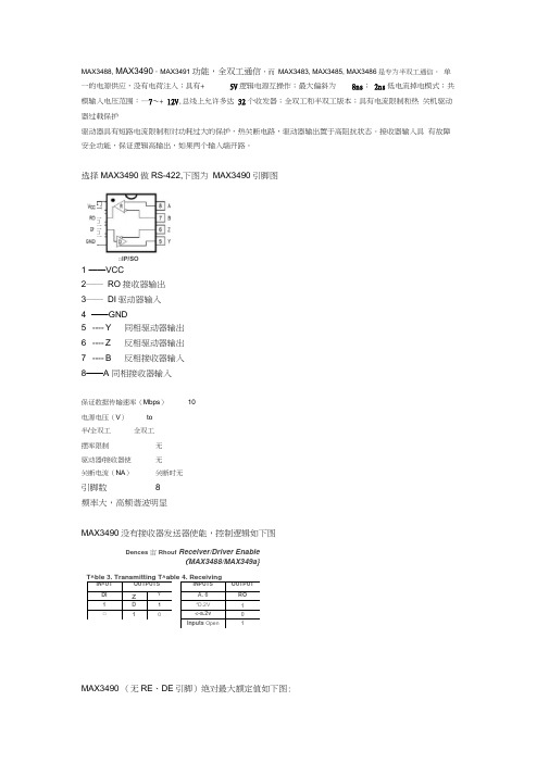
MAX3488, MAX3490,MAX3491 功能,全双工通信,而 MAX3483, MAX3485, MAX3486是专为半双工通信。
单一的电源供应,没有电荷注入;具有+ 5V 逻辑电源互操作;最大偏斜为 8ns ; 2ns 低电流掉电模式;共模输入电压范围:—7〜+ 12V ,总线上允许多达 32个收发器;全双工和半双工版本;具有电流限制和热 关机驱动器过载保护驱动器具有短路电流限制和对功耗过大的保护,热关断电路,驱动器输岀置于高阻抗状态。
接收器输入具 有故障安全功能,保证逻辑高输岀,如果两个输入端开路。
选择MAX3490做RS-422,下图为 MAX3490引脚图1 ——VCC2―― RO 接收器输出 3―― DI 驱动器输入 4 ——GND 5 ---- Y 同相驱动器输出 6 ---- Z 反相驱动器输出 7 ---- B反相接收器输入8——A 同相接收器输入保证数据传输速率(Mbps ) 10电源电压(V ) to 半/全双工 全双工摆率限制 无 驱动器/接收器使 无 关断电流(NA )关断时无引脚数8频率大,高频谐波明显MAX3490没有接收器发送器使能,控制逻辑如下图Dences 宙Rhouf Receiver/Driver Enable(MAX3488/MAX349a}T^ble 3. Transmitting T^able 4. ReceivingMAX3490 (无RE 、DE 引脚)绝对最大额定值如下图:IN^UTOUTPUTSDI zY 1 D 1 □1INPUTSOUTPUTA. 6 RO *D.2V1 <-a.2v0 Inputs Open1□IP/SOE L叵叵DABSOLUTE MAXIMUM RATINGSS U P P 卜F \ 01 ^3 9 e l\/ kill ■ ■ ■ ■ ■■!■■■■■■ iri ■ ■ ■ ■ ■ ■ ■ ■ ■ ■ ■ ■■ ■ ■ ■ ■ ■ i ■ ■ ■ r ■ ■ ■ ■ ■ ■ ■Control IrpiJ ValLage (RE, D£) ............... .......... ............... -0.3V ta 7V□rtvsr Inpul Voltage (6l).............. .......... .......... ............... -0.3Vtn 7VOnvar Output VcItaQ* (A,気V, ZX - ......................... -7J5V to12.SVftccer^CF Input VaKagc |A, B) . -7.5V to )2 5VReceiver Ojtput Voltage (RO) . . -O.3Vto (Vcc * 0 3V)Gontinucus Power g$ipmTk?n (T R= +70芒|各Pin Pi/Mc DIP 忖申rate 9 09mWU above +70© 72?mW8-Pin SO (<1HW 5 aarrrtVy «bove +7C P C), 471mW14-Rn Plastic DlP(de<m© 10mW fl C above +70忙》... HOOtrMf14-Rn SO (deia1^ fl.SSmW.^C abaw +70*C> __________ UUJllMfOperating Temperalur?MAXU C .............. ......... *........ ... ..................... -.Ot:to +7[TCMAX3d_ _E__”…lh.. “一,. ,.H.…““-“,-H.⑷乜B +85\:Storage Temperafur? Range lo +16[yCbead Tempeiature [wldering lOlMC)..................................... +XD*CMAX3490驱动器的开关特性如下图:DRIVER SWITCHING CHARACTERISTICS-MAX3465h MAX14$0, and MAX3491ri^E:» 3.3M a T*w *25*CJPARAMtFER CONCilTICNS m TVP MA 9(UNITSDrrwf OHtreftfiii OdljMjt Del叩g■ Sdll, Figure 7 122M mDrvcr Wfe-oEiii Ckrlp ui T M7»C r Time hno良L * fiOtl, Flpm 71&25mEtr p临他n M■丫LCfflMCHHiah Lrvtl IpiLM R L * 37(1. F4l/*a T2235m轉、ion Delay Hl0hi&-Lew Leveli IpML R. - ZTflFiflWWE■Jr22 35tp L n - iPHitl □越g*曲m Dtt&Ff吕的却iH^ie S- IPDS R.fc• 27n, FipL<eS E mDRIVER OUTPUT ENABLEJOIS^BLE TIMES {IWS-iflS'IMLW3-431 聞切Dmw CXJtput tnable r me I Q L OW LE^el tfZL Ri= 110SL f^FLFa 10 45 M OEDiwci" OulpiJl EiwN? Trne tg High Len el S FZH Ri ■ 110(1 钿ure $ 45raDrw CMp讥04»^le Time tom Migih Level fi t* 11(X1. F»flL*t940 to POriw D・*l・ Tim from LwLwi tpLE R L* 11IMI. i&40 BO mDTM< dip Lit Errtb^A Tiffii Au墟电叭旳Lx L#v4l tm Rl ■匚如i 10<8W gm 他Qrta&r ErrtBifi Titre frw 电靜©询|a H(;h 4PCH R; - 1inni FigiLiraS®o r»MAX3490CPA(TCto +70'Q8 Ptasttc DIPMAX349OCSA(TCt口+7D B C\8 SOMAX3490C/D crcto+70e c \Dice'MAX349OEPA-4(rc to +85X8 Plastic DIPMAX349OESA■40X10+9598 SOMAX3490引脚配置与典型工作电路,如下图|l巒4e 2 MAA J4ML JWAJC3啲Pin 8 两#挪询事呵Typ"C^ uftMOTE AEANODE O 8LXF砂*师悶ZKSQW诂沖盟F训卜皿咻斥$钵自Ncrv^OfU MAX3490封装尺寸L -15^ Plastic DIPPLASTIC DU AL-IN-LINE PACKAGE(0.300 in.)DIM [HOMES MLLlWETESS MIN MAA MIN MAXA a 200A1ocn&-■"20 12& C 175 3104-iS *3 0D5& Q0» 1.402W0.01S a 022 041 OKoo^ 1 MC DQOB0 0120200 30 &1D0Q&0 09001328E0.300 0 925 A2A E10咖0 310dia7VT e OJOO■■eA D.3H)■*tB Q4P0 10 16 L 0 IU a iso 2923J1 PINSMCHES MJJME1TER3-MN NUM MNI MAXa 0 3430 w BM 891 0140^3513-6719-43 ET lir o.-«Q -B51: 911&.43 010MBS 0i1522 4B 23.24 020 101S104535742454□24 1 14H2B52S DE37 13。
- 1、下载文档前请自行甄别文档内容的完整性,平台不提供额外的编辑、内容补充、找答案等附加服务。
- 2、"仅部分预览"的文档,不可在线预览部分如存在完整性等问题,可反馈申请退款(可完整预览的文档不适用该条件!)。
- 3、如文档侵犯您的权益,请联系客服反馈,我们会尽快为您处理(人工客服工作时间:9:00-18:30)。
_______________General DescriptionThe MAX4014/MAX4017/MAX4019/MAX4022 are preci-sion, closed-loop, gain of +2 (or -1) buffers featuring high slew rates, high output current drive, and low dif-ferential gain and phase errors. These single-supply devices operate from +3.15V to +11V, or from ±1.575V to ±5.5V dual supplies. The input voltage range extends 100mV beyond the negative supply rail and the outputs swing Rail-to-Rail ®.These devices require only 5.5mA of quiescent supply current while achieving a 200MHz -3dB bandwidth and a 600V/µs slew rate. I n addition, the MAX4019 has a disable feature that reduces the supply current to 400µA. I nput voltage noise for these parts is only 10nV/√Hz and input current noise is only 1.3pA/√Hz .This buffer family is ideal for low-power/low-voltage applications that require wide bandwidth, such as video, communications, and instrumentation systems.For space-sensitive applications, the MAX4014 comes in a tiny 5-pin SOT23 package.________________________ApplicationsPortable/Battery-Powered Instruments Video Line DriverAnalog-to-Digital Converter Interface CCD Imaging SystemsVideo Routing and Switching Systems____________________________Featureso Internal Precision Resistors for Closed-Loop Gains of +2 or -1o High Speed:200MHz -3dB Bandwidth30MHz 0.1dB Gain Flatness (6MHz min)600V/µs Slew Rate o Single 3.3V/5.0V Operation o Outputs Swing Rail-to-Railo Input Voltage Range Extends Beyond V EE o Low Differential Gain/Phase: 0.04%/0.02°o Low Distortion at 5MHz:-78dBc Spurious-Free Dynamic Range -75dB Total Harmonic Distortion o High Output Drive: ±120mA o Low, 5.5mA Supply Current o 400µA Shutdown Supply Currento Space-Saving SOT23-5, µMAX, or QSOP PackagesMAX4014/MAX4017/MAX4019/MAX4022Low-Cost, High-Speed, Single-Supply, Gain of +2Buffers with Rail-to-Rail Outputs in SOT23__________Typical Operating Circuit19-1284; Rev 2; 8/01_____________________Selector GuideRail-to-Rail is a registered trademark of Nippon Motorola Ltd.________________________________________________________________Maxim Integrated Products 1For pricing, delivery, and ordering information,please contact Maxim/Dallas Direct!at 1-888-629-4642, or visit Maxim’s website at .M A X 4014/M A X 4017/M A X 4019/M A X 4022Low-Cost, High-Speed, Single-Supply, Gain of +2 Buffers with Rail-to-Rail Outputs in SOT232_______________________________________________________________________________________ABSOLUTE MAXIMUM RATINGSDC ELECTRICAL CHARACTERISTICS(V CC = +5V, V EE = 0V, IN_- =0V, EN_ = 5V, R L = ∞to ground, V OUT = V CC / 2, noninverting configuration, T A = T MIN to T MAX , unless otherwise noted. Typical values are at T A = +25°C.) (Note 1)Supply Voltage (V CC to V EE )..................................................12V IN_-, IN_+, OUT_, EN_ ....................(V EE - 0.3V) to (V CC + 0.3V)Output Short-Circuit Duration to V CC or V EE ..............Continuous Continuous Power Dissipation (T A = +70°C)5-pin SOT23 (derate 7.1mW/°C above+70°C)..............571mW 8-pin SO (derate 5.9mW/°C above +70°C)...................471mW8-pin µMAX (derate 4.1mW/°C above +70°C)..............330mW 14-pin SO (derate 8.3mW/°C above +70°C).................667mW 16-pin QSOP (derate 8.3mW/°C above +70°C)............667mW Operating Temperature Range ...........................-40°C to +85°C Storage Temperature Range.............................-65°C to +150°C Lead Temperature (soldering, 10sec).............................+300°CStresses beyond those listed under “Absolute Maximum Ratings” may cause permanent damage to the device. These are stress ratings only, and functional operation of the device at these or at any other conditions beyond those indicated in the operational sections of the specifications is not implied. Exposure to absolute maximum rating conditions for extended periods may affect device reliability.MAX4014/MAX4017/MAX4019/MAX4022Low-Cost, High-Speed, Single-Supply, Gain of +2Buffers with Rail-to-Rail Outputs in SOT23_______________________________________________________________________________________3Note 1:The MAX4014EUK is 100% production tested at T A = +25°C. Specifications over temperature limits are guaranteed bydesign.Note 2:Tested with V OUT = +2.5V.Note 3: PSRR for single +5V supply tested with V EE = 0V, V CC = +4.5V to +5.5V; for dual ±5V supply with V EE = -4.5V to -5.5V,V CC = +4.5V to +5.5V; and for single +3V supply with V EE = 0V, V CC = +3.15V to +3.45V.Note 4:Guaranteed by design.AC ELECTRICAL CHARACTERISTICS(V CC = +5V, V EE = 0V, I N_- = 0V, EN_ = 5V, R L = 100Ωto ground, noninverting configuration, T A = T MIN to T MAX,unless otherwise noted. Typical values are at T A = +25°C.)M A X 4014/M A X 4017/M A X 4019/M A X 4022Low-Cost, High-Speed, Single-Supply, Gain of +2 Buffers with Rail-to-Rail Outputs in SOT234_______________________________________________________________________________________81100k1M10M 100M1G SMALL-SIGNAL GAIN vs. FREQUENCY3M A X 4014-01FREQUENCY (Hz)G A I N (d B )57246 6.86.75.9100k 1M 10M 100M 1GGAIN FLATNESS vs. FREQUENCYM A X 4014-02FREQUENCY (Hz)G A I N (d B )6.06.26.56.66.16.46.36780100k1M10M 100M1GLARGE-SIGNAL GAIN vs. FREQUENCY3M A X 4014-03FREQUENCY (Hz)G A I N (d B )521450-150100k1M10M 100M1GMAX4017/19/22CROSSTALK vs. FREQUENCY-110M A X 4014-04FREQUENCY (Hz)C R O S S T A L K (d B )-70-301030-130-90-50-100-10-20-30-60-70-90-80-40-50-100LOAD (Ω)2004006008001000HARMONIC DISTORTIONvs. LOADH A R M O N I C D I S T O R T I O N (d B c )10000.10.1M1M10M100MCLOSED-LOOP OUTPUT IMPEDANCEvs. FREQUENCYM A X 4014-05FREQUENCY (Hz)I M P E D A N C E (Ω)100110-100100k1M10M100MHARMONIC DISTORTION vs. FREQUENCY-80FREQUENCY (Hz)H A R M O N I C D I S T O R T I O N (d B c )-60-40-20-10-90-70-50-300-10-20-30-60-70-90-80-40-50-100OUTPUT SWING (Vp-p)0.51.0 1.52.0HARMONIC DISTORTION vs. OUTPUT SWINGH A R M O N I C D I S T O R T I O N (d B c )10-90100k10M100M1MMAX4019OFF ISOLATION vs. FREQUENCY-80M A X 4014-09FREQUENCY (Hz)O F F I S O L A T I O N (d B )-70-60-50-40-30-20-100 __________________________________________Typical Operating Characteristics(V CC = +5V, V EE = 0V, A VCL = +2, R L = 150Ωto V CC / 2, T A = +25°C, unless otherwise noted.)MAX4014/MAX4017/MAX4019/MAX4022Low-Cost, High-Speed, Single-Supply, Gain of +2Buffers with Rail-to-Rail Outputs in SOT23_______________________________________________________________________________________520-80100k1M10M100MPOWER-SUPPLY REJECTIONvs. FREQUENCY-60M A X 4014-10FREQUENCY (Hz)P O W E R -S U P P L Y R E J E C T I O N (d B )-40-20010-70-50-30-1076453M A X 4014-16TEMPERATURE (°C)-25-500755025100POWER-SUPPLY CURRENT (PER AMPLIFIER)vs. TEMPERATUREP O W E R -S U P P L Y C U R R E N T (m A)1011101k10M1MCURRENT NOISE DENSITYvs. FREQUENCYM A X 4014-11FREQUENCY (Hz)N O I S E (p A / H z )10010k 100k1001011101k10M1MVOLTAGE NOISE DENSITYvs. FREQUENCYM A X 4014-12FREQUENCY (Hz)N O I S E (n V /H z )10010k 100k52101001k10k100k1MOUTPUT SWING vs. LOAD RESISTANCEM A X 4014-13LOAD RESISTANCE (Ω)O U T P U T S W I N G (V p -p )344.54.03.52.52.01.53.01.0M A X 4014-14LOAD RESISTANCE (Ω)255075100125150OUTPUT SWINGvs. LOAD RESISTANCE (R L )O U T P U T S W I N G (V p -p )400350300250150501002000M A X 4014-15LOAD RESISTANCE (Ω)1000200500400300600BANDWIDTH vs. LOAD RESISTANCEB A N D W I D T H (M H z )6.05.54.55.04.0M A X 4014-17TEMPERATURE (°C)-25-500755025100INPUT BIAS CURRENT vs. TEMPERATUREI N P U T B I A S C U R R E N T (µA )0.200.160.120.040.080M A X 4014-18TEMPERATURE (°C)-25-500755025100INPUT OFFSET CURRENT vs. TEMPERATUREI N P U T O F F S E T C U R R E N T (µA )__________________________________________Typical Operating Characteristics(V CC = +5V, V EE = 0V, A VCL = +2, R L = 150Ωto V CC / 2, T A = +25°C, unless otherwise noted.)M A X 4014/M A X 4017/M A X 4019/M A X 4022Low-Cost, High-Speed, Single-Supply, Gain of +2 Buffers with Rail-to-Rail Outputs in SOT236_______________________________________________________________________________________1086420M A X 4014-19POWER-SUPPLY VOLTAGE (V)43567891011POWER-SUPPLY CURRENT (PER AMPLIFIER)vs. POWER-SUPPLY VOLTAGEP O W E R -S U P P L Y C U R R E N T (m A )5.04.84.64.24.44.0TEMPERATURE (°C)-25-500755025100VOLTAGE SWING vs. TEMPERATUREV O L T A G E S W I N G (V p -p )543120M A X 4014-20TEMPERATURE (°C)-25-500755025100INPUT OFFSET VOLTAGE vs. TEMPERATUREI N P U T O F F S E T V O L T A G E (m V )-0.025-0.020-0.015-0.010-0.0050.0000.0050.01001000100DIFFERENTIAL GAIN AND PHASE-0.05-0.04-0.02-0.03-0.010.000.01IRE IRED I F F . P H A SE (de g )D I F F . G A I N (%)M A X 4014-22IN OUTV O L T A G E(500m V /d i v )LARGE-SIGNAL PULSE RESPONSEMAX4014-25TIME (20ns/div)V CM = 0.9V, R L = 100Ω to GROUNDIN OUT V O L T A G E (25m V /d i v )SMALL-SIGNAL PULSE RESPONSEM A X 4014-23TIME (20ns/div)V CM = 1.25V, R L = 100Ω to GROUNDINOUTV O L T A G E (25m V /d i v )SMALL-SIGNAL PULSE RESPONSE(C L = 5pF)MAX4014-24TIME (20ns/div)INOUTV O L T A G E (500m V /d i v )LARGE-SIGNAL PULSE RESPONSE(C L = 5pF)MAX4014-26TIME (20ns/div)V CM = 1.75V, R L = 100Ω to GROUNDEN_5.0V (ENABLE)0V(DISABLE)1V0VOUTENABLE RESPONSE TIMEMAX4014-27TIME (1µs/div)V IN = 0.5V__________________________________________Typical Operating Characteristics(V CC = +5V, V EE = 0V, A VCL = +2, R L = 150Ωto V CC / 2, T A = +25°C, unless otherwise noted.)MAX4014/MAX4017/MAX4019/MAX4022Low-Cost, High-Speed, Single-Supply, Gain of +2Buffers with Rail-to-Rail Outputs in SOT23_______________________________________________________________________________________7______________________________________________________________Pin DescriptionM A X 4014/M A X 4017/M A X 4019/M A X 4022Low-Cost, High-Speed, Single-Supply, Gain of +2 Buffers with Rail-to-Rail Outputs in SOT238______________________________________________________________________________________________________Detailed DescriptionThe MAX4014/MAX4017/MAX4019/MAX4022 are sin-gle-supply, rail-to-rail output, voltage-feedback, closed-loop buffers that employ current-feedback techniques to achieve 600V/µs slew rates and 200MHz band-widths. These buffers use internal 500Ωresistors to provide a preset closed-loop gain of +2V/V in the non-inverting configuration or -1V/V in the inverting configu-ration. Excellent harmonic distortion and differential gain/phase performance make these buffers an ideal choice for a wide variety of video and RF signal-pro-cessing applications.Local feedback around the buffer’s output stage ensures low output impedance, which reduces gain sensitivity to load variations. This feedback also pro-duces demand-driven current bias to the output tran-sistors for ±120mA drive capability, while constraining total supply current to less than 7mA.__________Applications InformationPower SuppliesThese devices operate from a single +3.15V to +11V power supply or from dual supplies of ±1.575V to ±5.5V. For single-supply operation, bypass the V CC pin to ground with a 0.1µF capacitor as close to the pin as possible. If operating with dual supplies, bypass each supply with a 0.1µF capacitor.Selecting Gain ConfigurationEach buffer in the MAX4014 family can be configured for a voltage gain of +2V/V or -1V/V. For a gain of+2V/V, ground the inverting terminal. Use the noninvert-ing terminal as the signal input of the buffer (Figure 1a).Grounding the noninverting terminal and using the inverting terminal as the signal input configures the buffer for a gain of -1V/V (Figure 1b).Since the inverting input exhibits a 500Ωinput imped-ance, terminate the input with a 56Ωresistor when the device is configured for an inverting gain in 50Ωappli-cations (terminate with 88Ωin 75Ωapplications).Terminate the input with a 49.9Ωresistor in the nonin-verting case. Output terminating resistors should direct-ly match cable impedances in either configuration.Layout TechniquesMaxim recommends using microstrip and stripline tech-niques to obtain full bandwidth. To ensure that the PC board does not degrade the buffer’s performance, design it for a frequency greater than 1GHz. Pay careful attention to inputs and outputs to avoid large parasitic capaci-tance. Whether or not you use a constant-impedance board, observe the following guidelines when designing the board:•Don’t use wire-wrapped boards. They are too inductive.•Don’t use IC sockets. They increase parasitic capac-itance and inductance.•Use surface-mount instead of through-hole compon-ents for better high-frequency performance.•Use a PC board with at least two layers; it should be as free from voids as possible.•Keep signal lines as short and as straight as possi-ble. Do not make 90°turns; round all corners.Figure 1a. Noninverting Gain Configuration (A V = +2V/V)Figure 1b. Inverting Gain Configuration (A V = -1V/V)MAX4014/MAX4017/MAX4019/MAX4022Low-Cost, High-Speed, Single-Supply, Gain of +2Buffers with Rail-to-Rail Outputs in SOT23_______________________________________________________________________________________9Input Voltage Range and Output SwingThe input range for the MAX4014 family extends from (V EE - 100mV) to (V CC - 2.25V). I nput ground sensing increases the dynamic range for single-supply applica-tions. The outputs drive a 2k Ωload to within 60mV of the power-suply rails. With heavier loads, the output swing is reduced as shown in the Electrical Character-istics and the Typical Operating Characteristics . As the load increases, the input range is effectively limited bythe output-drive capability, since the buffers have a fixed voltage gain of +2 or -1.For example, a 50Ωload can typically be driven from 40mV above V EE to 1.6V below V CC , or 40mV to 3.4V when operating from a single +5V supply. If the buffer is operated in the noninverting, gain of +2 configuration with the inverting input grounded, the effective input voltage range becomes 20mV to 1.7V, instead of the -100mV to 2.75V indicated by the Electrical Character-istics . Beyond the effective input range, the buffer out-put is a nonlinear function of the input, but it will not undergo phase reversal or latchup.EnableThe MAX4019 has an enable feature (EN_) that allows the buffer to be placed in a low-power state. When the buffers are disabled, the supply current will not exceed 550µA per buffer.As the voltage at the EN_ pin approaches the negativesupply rail, the EN_ input current rises. Figure 2 shows a graph of EN_ input current versus EN_ pin voltage.Figure 3 shows the addition of an optional resistor in series with the EN pin, to limit the magnitude of the cur-rent increase. Figure 4 displays the resulting EN pin input current to voltage relationship.Figure 3. Circuit to Reduce Enable Logic-Low Input CurrentFigure 4. Enable Logic-Low Input Current vs. Enable Logic-Low Threshold with 10k ΩSeries ResistorM A X 4014/M A X 4017/M A X 4019/M A X 4022Low-Cost, High-Speed, Single-Supply, Gain of +2 Buffers with Rail-to-Rail Outputs in SOT2310______________________________________________________________________________________Disabled Output ResistanceThe MAX4014/MAX4017/MAX4019/MAX4022 include internal protection circuitry that prevents damage to the precision input stage from large differential input volt-ages, as shown in Figure 5. This protection circuitry con-sists of five back-to-back Schottky diodes between IN_+and IN_-. These diodes lower the disabled output resis-tance from 1k Ωto 500Ωwhen the output voltage is 3V greater or less than the voltage at I N_+. Under theseconditions, the input protection diodes will be forward biased, lowering the disabled output resistance to 500Ω.Output Capacitive Loading and StabilityThe MAX4014/MAX4017/MAX4019/MAX4022 provide maximum AC performance with no load capacitance.This is the case when the load is a properly terminated transmission line. However, they are designed to drive up 25pF of load capacitance without oscillating, but with reduced AC performance.Driving large capacitive loads increases the chance of oscillations occurring in most amplifier circuits. This is especially true for circuits with high loop gains, such as voltage followers. The buffer’s output resistance and the load capacitor combine to add a pole and excess phase to the loop response. I f the frequency of this pole is low enough to interfere with the loop response and degrade phase margin sufficiently, oscillations can occur.A second problem when driving capacitive loads results from the amplifier’s output impedance, which looks inductive at high frequencies. This inductance forms an L-C resonant circuit with the capacitive load,which causes peaking in the frequency response and degrades the amplifier’s gain margin.Figure 6 shows the frequency response of the MAX4014/MAX4017/MAX4019/MAX4022 under different capacitive loads. To drive loads with greater than 25pF of capaci-tance or to settle out some of the peaking, the output requires an isolation resistor like the one shown inFigure 5. Input Protection CircuitFigure 7. Driving a Capacitive Load through an Isolation ResistorMAX4014/MAX4017/MAX4019/MAX4022Low-Cost, High-Speed, Single-Supply, Gain of +2Buffers with Rail-to-Rail Outputs in SOT23______________________________________________________________________________________11Figure 8. Capacitive Load vs. Isolation ResistanceFigure 9. Small-Signal Gain vs. Frequency with Load Capacitance and 27ΩIsolation ResistorFigure 7. Figure 8 is a graph of the optimal isolation resis-tor versus load capacitance. Figure 9 shows the frequen-cy response of the MAX4014/MAX4017/MAX4019/MAX4022 when driving capacitive loads with a 27Ωisola-tion resistor.Coaxial cables and other transmission lines are easily dri-ven when properly terminated at both ends with their characteristic impedance. Driving back-terminated trans-mission lines essentially eliminates the lines’ capacitance.M A X 4014/M A X 4017/M A X 4019/M A X 4022Low-Cost, High-Speed, Single-Supply, Gain of +2 Buffers with Rail-to-Rail Outputs in SOT23Maxim cannot assume responsibility for use of any circuitry other than circuitry entirely embodied in a Maxim product. No circuit patent licenses are implied. Maxim reserves the right to change the circuitry and specifications without notice at any time.12____________________Maxim Integrated Products, 120 San Gabriel Drive, Sunnyvale, CA 94086 408-737-7600©2001 Maxim Integrated ProductsPrinted USAis a registered trademark of Maxim Integrated Products.__________________________________________________________Pin Configurations___________________Chip InformationSUBSTRATE CONNECTED TO V EE。