MAX4173HESA-T中文资料
MAX471MAX472的中文资料大全
M A X471M A X472的中文资料大全(总4页)-本页仅作为预览文档封面,使用时请删除本页-MAX471/MAX472的特点、功能美国美信公司生产的精密高端电流检测放大器是一个系列化产品,有MAX471/MA X472、 MAX4172/MAX4173等。
它们均有一个电流输出端,可以用一个电阻来简单地实现以地为参考点的电流/电压的转换,并可工作在较宽电压内。
MAX471/MAX472具有如下特点:●具有完美的高端电流检测功能;●内含精密的内部检测电阻(MAX471);●在工作温度范围内,其精度为2%;●具有双向检测指示,可监控充电和放电状态;●内部检测电阻和检测能力为3A,并联使用时还可扩大检测电流范围;●使用外部检测电阻可任意扩展检测电流范围(MAX472);●最大电源电流为100μA;●关闭方式时的电流仅为5μA;●电压范围为3~36V;●采用8脚DIP/SO/STO三种封装形式。
MAX471/MAX472的引脚排列如图1所示,图2所示为其内部功能框图。
表1为MAX471/MAX472的引脚功能说明。
MAX471的电流增益比已预设为500μA/A,由于2kΩ的输出电阻(ROUT)可产生1V/A的转换,因此±3A时的满度值为3V.用不同的ROUT电阻可设置不同的满度电压。
但对于MAX471,其输出电压不应大于VRS+。
对于MAX472,则不能大于。
MAX471引脚图如图1所示,MAX472引脚图如图2所示。
MAX471/MAX472的引脚功能说明引脚名称功能MAX471MAX47211SHDN关闭端。
正常运用时连接到地。
当此端接高电平时,电源电流小于5μA2,3-RS+内部电流检测电阻电池(或电源端)。
“+”仅指示与SIGN输出有关的流动方向。
封装时已将2和3连在了一起-2空脚-3RG1增益电阻端。
通过增益设置电阻连接到电流检测电阻的电池端44GND地或电池负端55SIGN集电极开路逻辑输出端。
MAX4173TEUT-T中文资料

Notebook Computers
Portable/Battery-Powered Systems
Smart Battery Packs/Chargers
Cell Phones
Power-Management Systems
General System/Board-Level Current Monitoring
The combination of three gain versions and a userselectable external sense resistor sets the full-scale current reading. This feature offers a high level of integration, resulting in a simple and compact currentsense solution.
+20V/V (MAX4173T) +50V/V (MAX4173F) +100V/V (MAX4173H) ♦ ±0.5% Full-Scale Accuracy ♦ ±0.3mV Input Offset Voltage (MAX4173T) ♦ 420µA Supply Current ♦ Wide 1.7MHz Bandwidth (MAX4173T) ♦ +3V to +28V Operating Supply ♦ Available in Space-Saving SOT23-6 Package
Typical Operating Circuit
0 TO +28V
VSENSE
+3V TO +28V 0.1µF
MAX1722EZK-T中文资料
MAX1722
FB 3
4
OUT
THIN SOT23-5
Pin Configurations are continued at end of data sheet.
________________________________________________________________ Maxim Integrated Products
元器件交易网
19-1735; Rev 0; 7/01
1.5µA IQ, Step-Up DC-DC Converters in Thin SOT23-5
General Description
The MAX1722/MAX1723/MAX1724 compact, high-efficiency, step-up DC-DC converters are available in tiny, 5pin thin SOT23 packages. They feature an extremely low 1.5µA quiescent supply current to ensure the highest possible light-load efficiency. Optimized for operation from one to two alkaline or nickel-metal-hydride (NiMH) cells, or a single Li+ cell, these devices are ideal for applications where extremely low quiescent current and ultra-small size are critical. Built-in synchronous rectification significantly improves efficiency and reduces size and cost by eliminating the need for an external Schottky diode. All three devices feature a 0.5Ω N-channel power switch. The MAX1722/ MAX1724 also feature proprietary noise-reduction circuitry, which suppresses electromagnetic interference (EMI) caused by the inductor in many step-up applications. The family offers different combinations of fixed or adjustable outputs, shutdown, and EMI reduction (see Selector Guide). o o o o o o o o o o o
17431资料

To all our customersRegarding the change of names mentioned in the document, such as Hitachi Electric and Hitachi XX, to Renesas Technology Corp.The semiconductor operations of Mitsubishi Electric and Hitachi were transferred to Renesas Technology Corporation on April 1st 2003. These operations include microcomputer, logic, analog and discrete devices, and memory chips other than DRAMs (flash memory, SRAMs etc.) Accordingly, although Hitachi, Hitachi, Ltd., Hitachi Semiconductors, and other Hitachi brand names are mentioned in the document, these names have in fact all been changed to Renesas Technology Corp. Thank you for your understanding. Except for our corporate trademark, logo and corporate statement, no changes whatsoever have been made to the contents of the document, and these changes do not constitute any alteration to the contents of the document itself.Renesas Technology Home Page: Renesas Technology Corp.Customer Support Dept.April 1, 2003CautionsKeep safety first in your circuit designs!1. Renesas Technology Corporation puts the maximum effort into making semiconductor products betterand more reliable, but there is always the possibility that trouble may occur with them. Trouble with semiconductors may lead to personal injury, fire or property damage.Remember to give due consideration to safety when making your circuit designs, with appropriate measures such as (i) placement of substitutive, auxiliary circuits, (ii) use of nonflammable material or (iii) prevention against any malfunction or mishap.Notes regarding these materials1. These materials are intended as a reference to assist our customers in the selection of the RenesasTechnology Corporation product best suited to the customer's application; they do not convey any license under any intellectual property rights, or any other rights, belonging to Renesas Technology Corporation or a third party.2. Renesas Technology Corporation assumes no responsibility for any damage, or infringement of anythird-party's rights, originating in the use of any product data, diagrams, charts, programs, algorithms, or circuit application examples contained in these materials.3. All information contained in these materials, including product data, diagrams, charts, programs andalgorithms represents information on products at the time of publication of these materials, and are subject to change by Renesas Technology Corporation without notice due to product improvements or other reasons. It is therefore recommended that customers contact Renesas Technology Corporation or an authorized Renesas Technology Corporation product distributor for the latest product information before purchasing a product listed herein.The information described here may contain technical inaccuracies or typographical errors.Renesas Technology Corporation assumes no responsibility for any damage, liability, or other loss rising from these inaccuracies or errors.Please also pay attention to information published by Renesas Technology Corporation by various means, including the Renesas Technology Corporation Semiconductor home page().4. When using any or all of the information contained in these materials, including product data, diagrams,charts, programs, and algorithms, please be sure to evaluate all information as a total system before making a final decision on the applicability of the information and products. Renesas Technology Corporation assumes no responsibility for any damage, liability or other loss resulting from theinformation contained herein.5. Renesas Technology Corporation semiconductors are not designed or manufactured for use in a deviceor system that is used under circumstances in which human life is potentially at stake. Please contact Renesas Technology Corporation or an authorized Renesas Technology Corporation product distributor when considering the use of a product contained herein for any specific purposes, such as apparatus or systems for transportation, vehicular, medical, aerospace, nuclear, or undersea repeater use.6. The prior written approval of Renesas Technology Corporation is necessary to reprint or reproduce inwhole or in part these materials.7. If these products or technologies are subject to the Japanese export control restrictions, they must beexported under a license from the Japanese government and cannot be imported into a country other than the approved destination.Any diversion or reexport contrary to the export control laws and regulations of Japan and/or thecountry of destination is prohibited.8. Please contact Renesas Technology Corporation for further details on these materials or the productscontained therein.HA17431 SeriesShunt RegulatorADE-204-049A (Z)Rev.1Sep. 2002 DescriptionThe HA17431 series is temperature-compensated variable shunt regulators. The main application of these products is in voltage regulators that provide a variable output voltage. The on-chip high-precisionmax of 16 volts. reference voltage source can provide ±1% accuracy in the V versions, which have a VKAThe HA17431VLP, which is provided in the MPAK-5 package, is designed for use in switching mode power supplies. It provides a built-in photocoupler bypass resistor for the PS pin, and an error amplifier can be easily constructed on the supply side.Features•The V versions provide 2.500 V ±1% at Ta = 25°C•The HA17431VLP includes a photocoupler bypass resistor (2 kΩ)•The reference voltage has a low temperature coefficient•The MPAK-5(5-pin), MPAK(3-pin) and UPAK miniature packages are optimal for use on high mounting density circuit boards•Car use is providedBlock DiagramHA17431 SeriesRev.1, Sep. 2002, page 2 of 24Application Circuit ExampleOrdering InformationVersionItemV VersionA Version Normal VersionPackage Operating Temperature Range Accuracy ±1% ±2.2% ±4% Max 2.525 V 2.550 V 2.595 V Typ 2.500 V 2.495 V 2.495 V Reference voltage (at 25°C)Min2.475 V 2.440 V 2.395 V Cathode voltage 16 V max 40 V max 40 V max Cathode current 50 mA max150 mA max150 mA maxHA17431VPJHA17431PNAJTO-92HA17431PAJ HA17431PJ TO-92MOD HA17431FPAJ Car useHA17431FPJFP-8D –40 to +85°CHA17431 SeriesRev.1, Sep. 2002, page 3 of 24Ordering Information (cont.)VersionItemV VersionA VersionNormal VersionPackage Operating Temperature Range HA17431VLTP HA17432VLTP MPAKHA17431VLP MPAK-5 HA17431VP HA17431PNA TO-92 HA17431VUP HA17431UPA HA17432VUPHA17432UPAUPAK HA17431PA HA17431P TO-92MOD HA17431FPA Industrial useHA17431FPFP-8D HA17431UA Commercial use HA17432UAUPAK –20 to +85°CPin ArrangementHA17431 SeriesRev.1, Sep. 2002, page 4 of 24Absolute Maximum Ratings(Ta = 25°C)Item Symbol HA17431VLP HA17431VP HA17431VPJ Unit Notes Cathode voltage V KA 16 16 16 V 1 PS term. voltage V PS V KA to 16 — — V 1,2,3Continuous cathode current I K –50 to +50 –50 to +50 –50 to +50 mA Reference input currentIref–0.05 to +10–0.05 to +10–0.05 to +10mAPower dissipation P T 150 *4 500 *5 500 *5 mW 4, 5 Operating temperature range Topr–20 to +85–20 to +85–40 to +85°CStorage temperatureTstg –55 to +150 –55 to +150 –55 to +150 °CItem Symbol HA17431VUP/HA17432VUP HA17431VLTP/HA17432VLTP Unit Notes Cathode voltage V KA 16 16V 1PS term. voltage V PS — — V 1,2,3 Continuouscathode current I K –50 to +50 –50 to +50 mA Reference input currentIref–0.05 to +10–0.05 to +10mAPower dissipation P T 800 *8 150 *4 mW 4, 8 Operating temperature range Topr–20 to +85–20 to +85°CStorage temperatureTstg –55 to +150 –55 to +150 °CItemSymbol HA17431PNA HA17431P/PAHA17431FP/FPA HA17431UA/UPA/ HA17432UA/UPAUnitNotes Cathode voltage V KA 4040 40 40 V 1Continuous cathode current I K –100 to +150 –100 to +150 –100 to +150 –100 to +150 mA Reference input currentIref–0.05 to +10–0.05 to +10–0.05 to +10–0.05 to +10mAPower dissipation P T 500 *5 800 *6 500 *7 800 *8 mW 5,6,7,8 Operating temperature range Topr–20 to +85–20 to +85–20 to +85–20 to +85°CStorage temperatureTstg –55 to +150 –55 to +150 –55 to +125 –55 to +150 °CHA17431 SeriesRev.1, Sep. 2002, page 5 of 24Absolute Maximum Ratings (cont.)(Ta = 25°C)Item Symbol HA17431PNAJ HA17431PJ/PAJ HA17431FPJ/FPAJ Unit Notes Cathode voltage V KA 40 40 40 V 1 Continuous cathode current I K –100 to +150 –100 to +150 –100 to +150 mA Reference input currentIref–0.05 to +10–0.05 to +10–0.05 to +10mAPower dissipation P T 500 *5 800 *6 500 *7 mW 5,6,7 Operating temperature range Topr–40 to +85–40 to +85–40 to +85°CStorage temperatureTstg –55 to +150 –55 to +150 –55 to +125 °CNotes: 1. Voltages are referenced to anode.2. The PS pin is only provided by the HA17431VLP.3. The PS pin voltage must not fall below the cathode voltage. If the PS pin is not used, the PS pinis recommended to be connected with the cathode.4. Ta ≤ 25°C. If Ta > 25°C, derate by 1.2 mW/°C.5. Ta ≤ 25°C. If Ta > 25°C, derate by 4.0 mW/°C.6. Ta ≤ 25°C. If Ta > 25°C, derate by 6.4 mW/°C.7. 50 mm × 50 mm × 1.5mmt glass epoxy board(5% wiring density), Ta ≤ 25°C. If Ta > 25°C,derate by 5 mW/°C.8. 15 mm × 25 mm × 0.7mmt alumina ceramic board,Ta ≤ 25°C. If Ta > 25°C, derate by 6.4mW/°C.HA17431 SeriesRev.1, Sep. 2002, page 6 of 24Electrical CharacteristicsHA17431VLP/VP/VPJ/VUP/VLTP, HA17432VUP/VLTP (Ta = 25°C, I K = 10 mA)Item Symbol Min Typ Max Unit Test Conditions Notes Reference voltage Vref 2.475 2.500 2.525 VV KA = VrefReference voltage temperature deviationVref(dev)— 10 — mV V KA = Vref,Ta = –20°C to +85°C 1Reference voltage temperature coefficient ∆Vref/∆Ta— ±30 — ppm/°C V KA = Vref,0°C to 50°C gradientReference voltage regulation ∆Vref/∆V KA — 2.0 3.7 mV/V V KA = Vref to 16 V Reference input currentIref — 2 6 µA R 1 = 10 k Ω, R 2 = ∞ Reference current temperature deviation Iref(dev)— 0.5 —µA R 1 = 10 k Ω, R 2 = ∞,Ta = –20°C to +85°CMinimum cathode currentImin — 0.4 1.0 mA V KA = Vref2 Off state cathode current Ioff — 0.001 1.0 µA V KA = 16 V, Vref = 0 V Dynamic impedance Z KA — 0.2 0.5 Ω V KA = Vref,I K = 1 mA to 50 mA Bypass resistance R PS 1.6 2.0 2.4 k ΩI PS = 1 mA3 Bypass resistance temperature coefficient ∆R PS /∆Ta— +2000 — ppm/°C I PS = 1 mA,0°C to 50°C gradient3HA17431 SeriesRev.1, Sep. 2002, page 7 of 24Electrical Characteristics (cont.)HA17431PJ/PAJ/FPJ/FPAJ/P/PA/UA/UPA/FP/FPA/PNA/PNAJ, HA17432UA/UPA (Ta = 25°C, I K = 10 mA)Item Symbol Min Typ Max Unit Test Conditions Notes 2.440 2.495 2.550 A Reference voltage Vref 2.395 2.495 2.595 V V KA = Vref Normal —11(30)Ta =–20°C to +85°C 1, 4Reference voltage temperature deviationVref(dev)— 5 (17)mV V KA = VrefTa = 0°C to +70°C1, 4 — 1.4 3.7 V KA = Vref to 10 V Reference voltage regulation ∆Vref/∆V KA — 1 2.2mV/V V KA = 10 V to 40 VReference input currentIref — 3.8 6 µA R 1 = 10 k Ω, R 2 = ∞ Reference current temperature deviation Iref(dev)— 0.5 (2.5) µA R 1 = 10 k Ω, R 2 = ∞,Ta = 0°C to +70°C 4Minimum cathode currentImin — 0.4 1.0 mA V KA = Vref2 Off state cathode current Ioff — 0.001 1.0 µA V KA = 40 V, Vref = 0 V Dynamic impedanceZ KA— 0.2 0.5 ΩV KA = Vref,I K = 1 mA to 100 mANotes: 1. Vref(dev) = Vref(max) – Vref(min)2. Imin is given by the cathode current at Vref = Vref (IK=10mA) – 15 mV.3. R PS is only provided in HA17431VLP.4. The maximum value is a design value (not measured).HA17431 SeriesRev.1, Sep. 2002, page 8 of 24MPAK-5(5-pin), MPAK(3-pin) and UPAK Marking PatternsThe marking patterns shown below are used on MPAK-5, MPAK and UPAK products. Note that the product code and mark pattern are different. The pattern is laser-printed.Notes: 1. Boxes (1) to (5) in the figures show the position of the letters or numerals, and are not actuallymarked on the package.2. The letters (1) and (2) show the product specific mark pattern.Product (1)(2) HA17431VLP 4 P HA17431VUP 4 R HA17432VUP 4 S HA17431VLTP 3 A HA17432VLTP 3 B HA17431UA 4 A HA17431UPA 4 B HA17432UA 4 C HA17432UPA 4F3. The letter (3) shows the production year code (the last digit of the year) for UPAK products.4. The bars (a), (b) and (c) show a production year code for MPAK-5 and MPAK products as shownbelow. After 2010 the code is repeated every 8 years.Year 2002 2003 2004 2005 2006 2007 2008 2009 (a) None None None Bar Bar Bar Bar None (b) None Bar Bar None None Bar Bar None (c) Bar None Bar None Bar None Bar None5. The letter (4) shows the production month code (see table below).Production month Jan. Feb. Mar. Apr. May. Jun. Jul. Aug. Sep. Oct. Nov. Dec. Marked code A B C D E F G H J K L M6. The letter (5) shows manufacturing code. For UPAK products.Characteristics CurvesHA17431VLP/VP/VPJ/VUP/VLTP, HA17432VUP/VLTPHA17431PJ/PAJ/FPJ/FPAJ/P/PA/UA/UPA/FP/FPA/PNA/PNAJ, HA17432UA/UPAApplication ExamplesAs shown in the figure on the right, this IC operates as an inverting amplifier, with the REF pin as input pin. The open-loop voltage gain is given by the reciprocal of “reference voltage deviation by cathodevoltage change ” in the electrical specifications, and is approximately 50 to 60 dB. The REF pin has a high input impedance, with an input current Iref of 3.8 µA Typ (V version: Iref = 2 µA Typ). The outputimpedance of the output pin K (cathode) is defined as dynamic impedance Z KA , and Z KA is low (0.2 Ω) over a wide cathode current range. A (anode) is used at the minimum potential, such as ground.Figure 1 Operation DiagramApplication HintsNo. Application Example Description1Reference voltage generation circuitVoutGND VinGNDThis is the simplest reference voltage circuit. The valueof the resistance R is set so that cathode current I K ≥ 1 mA.Output is fixed at Vout ≅ 2.5 V.The external capacitor C L (C L ≥ 3.3 µF) is used to prevent oscillation in normal applications.2 Variable output shunt regulator circuitThis is circuit 1 above with variable output provided.Vout ≅ 2.5 V ×Here,(R 1 + R 2)R 2Since the reference input current Iref = 3.8 µA Typ (V version: Iref = 2 µA Typ) flows through R 1, resistance values are chosen to allow the resultant voltage drop to be ignored.3Single power supply invertingcomparator circuitThis is an inverting type comparator with an input threshold voltage of approximately 2.5 V. Rin is the REF pin protection resistance, with a value of several k Ω to several tens of k Ω.R L is the load resistance, selected so that the cathode current I K • 1 mA when Vout is low.Condition C1C2Vin Less then 2.5 V 2.5 V or moreVout V CC (V OH )Approx. 2 V (V OL )ICOFF ON4 AC amplifier circuitGain G =(DC gain)R 1R 2 // R 3Cutoff frequency fc =12π Cf (R 1 // R 2 // R 3)This is an AC amplifier with voltage gain G = –R 1 / (R 2//R 3). The input is cut by capacitance Cin, so that the REF pin is driven by the AC input signal, centered on 2.5 V DC .R 2 also functions as a resistance that determines the DC cathode potential when there is no input, but if the input level is low and there is no risk of Vout clipping to V CC , this can be omitted.To change the frequency characteristic, Cf should be connected as indicated by the dotted line.5Switching power supply erroramplification circuit12Note:LED R3R4: Light emitting diode in photocoupler : Bypass resistor to feed IK(>Imin) when LED current vanishes : LED protection resistanceThis circuit performs control on the secondary side of a transformer, and is often used with a switching power supply that employs a photocoupler for offlining.The output voltage (between V+ and V –) is given by the following formula:Vout ≅ 2.5 V ×(R 1 + R 2)R 2In this circuit, the gain with respect to the Vout error is as follows:G =×R 2(R 1 + R 2)HA17431 open loop gain ×photocoupler total gainAs stated earlier, the HA17431 open-loop gain is 50 to60 dB.6Constant voltage regulator circuitV CCVoutGNDGNDThis is a 3-pin regulator with a discrete configuration, inwhich the output voltageVout = 2.5 V ×(R 2 + R 3)R 3R 1 is a bias resistance for supplying the HA17431 cathode current and the output transistor Q base current.7Discharge type constant current circuitV SI LThis circuit supplies a constant current ofI L ≅[A] into the load. Caution is required2.5 V R Ssince the HA17431 cathode current is also superimposed on IL .The requirement in this circuit is that the cathode current must be greater than Imin = 1 mA. The I Lsetting therefore must be on the order of several mA or more.8Induction type constant current circuitV I L SIn this circuit, the load is connected on the collector side of transistor Q in circuit 7 above. In this case, the load floats from GND, but the HA17431 cathode current is not superimposed on I L , so that I L can be kept small (1 mA or less is possible). The constant current value is the same as for circuit 7 above:I L ≅[A]2.5 V R SDesign Guide for AC-DC SMPS (Switching Mode Power Supply)Use of Shunt Regulator in Transformer Secondary Side ControlThis example is applicable to both forward transformers and flyback transformers. A shunt regulator is used on the secondary side as an error amplifier, and feedback to the primary side is provided via a photocoupler.Figure 2 Typical Shunt Regulator/Error AmplifierDetermination of External Constants for the Shunt RegulatorDC characteristic determination: In figure 2, R1 and R2are protection resistor for the light emitting diodein the photocoupler, and R2 is a bypass resistor to feed IKminimum, and these are determined as shownbelow. The photocoupler specification should be obtained separately from the manufacturer. Using the parameters in figure 2, the following formulas are obtained:R1 =V0– V F– V KI F + I B, R2 =V FI BVKis the HA17431 operating voltage, and is set at around 3 V, taking into account a margin for fluctuation.R2 is the current shunt resistance for the light emitting diode, in which a bias current IBof around 1/5 IFflows.Next, the output voltage can be determined by R3 and R4, and the following formula is obtained:V0 =R3 + R4R4× Vref, Vref = 2.5 V TypThe absolute values of R3 and R4are determined by the HA17431 reference input current Iref and the ACcharacteristics described in the next section. The Iref value is around 3.8 µA Typ. (V version: 2 µA Typ)AC characteristic determination: This refers to the determination of the gain frequency characteristic of the shunt regulator as an error amplifier. Taking the configuration in figure 2, the error amplifier characteristic is as shown in figure 3.Figure 3 HA17431 Error Amplification CharacteristicIn Figure 3, the following formulas are obtained: GainG 1 = G 0 ≈ 50 dB to 60 dB (determined by shunt regulator)G 2 =R 5R 3Corner frequenciesf 1 = 1/(2π C 1 G 0 R 3) f 2 = 1/(2π C 1 R 5)G 0 is the shunt regulator open-loop gain; this is given by the reciprocal of the reference voltage fluctuation ∆Vref/∆V KA , and is approximately 50 dB.Practical ExampleConsider the example of a photocoupler, with an internal light emitting diode V F = 1.05 V and I F = 2.5 mA, power supply output voltage V 2 = 5 V, and bias resistance R 2 current of approximately 1/5 I F at 0.5 mA. If the shunt regulator V K = 3 V, the following values are found.R 1 =5V – 1.05V – 3V2.5mA + 0.5mA= 316(Ω) (330Ω from E24 series)R 2 =1.05V0.5mA= 2.1(k Ω) (2.2k Ω from E24 series)Next, assume that R 3 = R 4 = 10 k Ω. This gives a 5 V output. If R 5 = 3.3 k Ω and C 1 = 0.022 µF, the following values are found.G 2 = 3.3 k Ω / 10 k Ω = 0.33 times (–10 dB) f 1 = 1 / (2 × π × 0.022 µF × 316 × 10 k Ω) = 2.3 (Hz) f 2 = 1 / (2 × π × 0.022 µF × 3.3 k Ω) = 2.2 (kHz)Package DimensionsDisclaimer1. Hitachi neither warrants nor grants licenses of any rights of Hitachi’s or any third party’s patent,copyright, trademark, or other intellectual property rights for information contained in this document. Hitachi bears no responsibility for problems that may arise with third party’s rights, including intellectual property rights, in connection with use of the information contained in this document. 2.Products and product specifications may be subject to change without notice. Confirm that you have received the latest product standards or specifications before final design, purchase or use.3. Hitachi makes every attempt to ensure that its products are of high quality and reliability. However, contact Hitachi’s sales office before using the product in an application that demands especially high quality and reliability or where its failure or malfunction may directly threaten human life or cause risk of bodily injury, such as aerospace, aeronautics, nuclear power, combustion control, transportation, traffic, safety equipment or medical equipment for life support.4. Design your application so that the product is used within the ranges guaranteed by Hitachi particularly for maximum rating, operating supply voltage range, heat radiation characteristics, installationconditions and other characteristics. Hitachi bears no responsibility for failure or damage when used beyond the guaranteed ranges. Even within the guaranteed ranges, consider normally foreseeable failure rates or failure modes in semiconductor devices and employ systemic measures such as fail-safes, so that the equipment incorporating Hitachi product does not cause bodily injury, fire or other consequential damage due to operation of the Hitachi product. 5. This product is not designed to be radiation resistant.6. No one is permitted to reproduce or duplicate, in any form, the whole or part of this document without written approval from Hitachi.7. Contact Hitachi’s sales office for any questions regarding this document or Hitachi semiconductor products.Sales OfficesHitachi, Ltd.Semiconductor & Integrated CircuitsNippon Bldg., 2-6-2, Ohte-machi, Chiyoda-ku, Tokyo 100-0004, Japan Tel: (03) 3270-2111 Fax: (03) 3270-5109Copyright © Hitachi, Ltd., 2002. All rights reserved. Printed in Japan.Hitachi Asia Ltd. Hitachi Tower16 Collyer Quay #20-00 Singapore 049318Tel : <65>-6538-6533/6538-8577 Fax : <65>-6538-6933/6538-3877URL : .sg URL /Hitachi Asia Ltd.(Taipei Branch Office)4/F, No. 167, Tun Hwa North Road Hung-Kuo Building Taipei (105), Taiwan Tel : <886>-(2)-2718-3666 Fax : <886>-(2)-2718-8180 Telex : 23222 HAS-TPURL : Hitachi Asia (Hong Kong) Ltd.Group III (Electronic Components) 7/F., North TowerWorld Finance Centre,Harbour City, Canton RoadTsim Sha Tsui, Kowloon Hong Kong Tel : <852>-2735-9218 Fax : <852>-2730-0281URL : Hitachi Europe GmbHElectronic Components Group Dornacher Straße 3D-85622 FeldkirchenPostfach 201, D-85619 Feldkirchen GermanyTel: <49> (89) 9 9180-0Fax: <49> (89) 9 29 30 00Hitachi Europe Ltd.Electronic Components Group Whitebrook ParkLower Cookham Road MaidenheadBerkshire SL6 8YA, United Kingdom Tel: <44> (1628) 585000Fax: <44> (1628) 585200Hitachi Semiconductor (America) Inc.179 East Tasman Drive San Jose,CA 95134 Tel: <1> (408) 433-1990Fax: <1>(408) 433-0223For further information write to:Colophon 6.0。
基于CPLD的实时电流检测系统设计
225电力电子Power Electronic电子技术与软件工程Electronic Technology & Software Engineering随着电子技术的发展,在各种电子设备中,对功耗的要求越来越严格,已知电压和电流的话即可计算出器件功耗。
本文介绍一种简便的电流检测方法,通过精密电阻将电流值转换为电压值,然后通过电流传感放大电路,将电压值放大,再将放大后的电压值通过A/D 芯片转换为数字信号,A/D 芯片数字端的接口为常用的SPI 接口,CPLD 处理器可以通过SPI 总线方便的读取出量化后的数值,进而推算出相应的电流值,然后通过串口反馈给上位机。
1 电流检测电路组成如图1所示,电源转换芯片输出端和负载电源输入端之间串联一个10mΩ的精密电阻,因为电流一般较小,所以经过一个信号放大芯片MAX4173,将信号放大20倍,再经过一个运算放大器LM124J 实现隔离,最后接到ADC 芯片ADS8661上。
ADS8661通过SPI 总线与CPLD 连接,CPLD 通过串口转USB 芯片CP2103与主机连接,在主机上通过上位机软件方便的读取电流值。
1.1 电流传感放大电路电流传感放大电路如图2所示,选用的芯片型号为MAX4173。
MAX4173是一种低成本、高精度的电流传感放大器,采用小型SOT23-6封装,增益为20倍。
MAX4173采用+3V 至+28V 单电源供电,通常只消耗420uA 的电源电流。
1.2 隔离电路为了实现电流传感放大电路和后级A/D 电路的隔离,中间加了运算放大器电路实现信号的隔离,运算放大器选择常用的TI 公司的LM124J ,按照电压跟随器的解法进行连接。
电压跟随器的输入阻抗高,而输出阻抗低。
一般来说,输入阻抗可以达到几兆欧姆,而输出阻抗低,通常只有几欧姆,甚至更低。
电压隔离器输出电压近似输入电压幅度,并对前级电路呈高阻状态,对后级电路呈低阻状态,因而对前后级电路起到隔离作用。
赛米控丹佛斯 SEMITRANS 全碳化硅功率模块 SKM260MB170SCH17 数据表
© by SEMIKRONRev. 1.0–04.11.20201SEMITRANS ®3SiC MOSFET ModuleSKM260MB170SCH17Features*•Full Silicon Carbide (SiC) power module•High reliability 2nd Generation SiC MOSFETs•Optimized for fast switching and lowest power losses•External SiC Schottky Barrier Diode embedded•Insulated copper baseplate using DBC technology (Direct Bonded Copper)•Improved thermal performances with Aluminum Nitride (AlN) substrate •UL recognized, file no. E63532Typical Applications•High frequency power supplies •AC inverters •Traction APU •EV Chargers•Industrial Test SystemsRemarks•Case temperature limited to T C = 125°C max.•Recommended T jop = -40 ... +150°C •Gate-Source SURGE VOLTAGE(t surge <300ns), V GS_surge = -10V ... +26VAbsolute Maximum Ratings SymbolConditions Values UnitMOSFET V DSS T j =25°C 1700VI D T j =175°CT c =25°C 378 A T c =80°C301 A I DMPW ≤ 10µs, Duty cycle ≤ 1%980A I DM,repetitive790A V GS -6...22V T j-40 (175)°CAbsolute Maximum Ratings SymbolConditionsValuesUnitInverse diodeV RRM T j =25°C 1700V I F T j =175°CT c =25°C 552A T c =80°C428A I Fnom 300A I FRM 900A I FSM t p =10ms, sin 180°, T j =150°C, including body diode2030A T j-40 (175)°CAbsolute Maximum Ratings SymbolConditions Values UnitModule I t(RMS)500A T stg module without TIM -40...125°C V isolAC sinus 50 Hz, t =1min4000V2Rev. 1.0–04.11.2020© by SEMIKRONSEMITRANS ®3SiC MOSFET ModuleSKM260MB170SCH17Features*•Full Silicon Carbide (SiC) power module•High reliability 2nd Generation SiC MOSFETs•Optimized for fast switching and lowest power losses•External SiC Schottky Barrier Diode embedded•Insulated copper baseplate using DBC technology (Direct Bonded Copper)•Improved thermal performances with Aluminum Nitride (AlN) substrate •UL recognized, file no. E63532Typical Applications•High frequency power supplies •AC inverters •Traction APU •EV Chargers•Industrial Test SystemsRemarks•Case temperature limited to T C = 125°C max.•Recommended T jop = -40 ... +150°C •Gate-Source SURGE VOLTAGE(t surge <300ns), V GS_surge = -10V ... +26VMOSFET V (BR)DSS V GS =0V,I D =1mA, T j =25°C 1700V V GS(th)V DS =V GS , I D =57.75mA1.62.84V I DSS V GS =0V,V DS =1700V, T j =25°C 1.8mA I GSS V GS =22V,V DS =0V 700nA R DS(on)V GS =18V I D =161AchiplevelT j =25°C 8.110m ΩT j =150°C 14m ΩC iss V GS =0V V DS =800Vf =1MHzT j =25°C 27nF C oss T j =25°C 0.88nF C rss T j =25°C0.105nF R Gint T j =25°C2.1ΩQ G V DD =1000V, V GS =-5 ... 20V, I D =300A 1470nC t d(on)V DD =900V I D =300A V GS =-5 / +20VR Gon =0.7ΩR Goff =0.7Ωdi/dt on =12kA/µs di/dt off =9.5kA/µsdv/dt off =22kV/µs T j =150°C 64ns t r T j =150°C 60ns t d(off)T j =150°C162ns t f T j =150°C 32ns E on T j =150°C 7.59mJ E off T j =150°C6.21mJ R th(j-c)per MOSFET0.065K/W R th(c-s)per MOSFET (λgrease =0.81 W/(m*K))0.03K/WCharacteristics SymbolConditionsmin.typ.max.UnitInverse diodeV F = V SD I F =300A chiplevel T j =25°C 1.65 1.95V T j =150°C 2.51 2.86V V F0chiplevel T j =25°C 1.00 1.10V T j =150°C 0.860.96V r F chiplevelT j =25°C2.2 2.8m ΩT j =150°C5.56.3m ΩC j parallel to C oss , f =1MHz, V R =1700V, T j =25°C1.026nF Q c V R =800V, di/dt off =500A/µs, T j =25°C 0.95µCR th(j-c)per diode0.056K/W R th(c-s)per diode (λgrease =0.81 W/(m*K))0.027K/W© by SEMIKRONRev. 1.0–04.11.20203SEMITRANS ®3SiC MOSFET ModuleSKM260MB170SCH17Features*•Full Silicon Carbide (SiC) power module•High reliability 2nd Generation SiC MOSFETs•Optimized for fast switching and lowest power losses•External SiC Schottky Barrier Diode embedded•Insulated copper baseplate using DBC technology (Direct Bonded Copper)•Improved thermal performances with Aluminum Nitride (AlN) substrate •UL recognized, file no. E63532Typical Applications•High frequency power supplies •AC inverters •Traction APU •EV Chargers•Industrial Test SystemsRemarks•Case temperature limited to T C = 125°C max.•Recommended T jop = -40 ... +150°C •Gate-Source SURGE VOLTAGE(t surge <300ns), V GS_surge = -10V ... +26VModule L DS 15nH R DD'+SS'measured per switchT C =25°C0.55m ΩT C =125°C0.85m ΩR th(c-s)1calculated without thermal coupling (λgrease =0.81 W/(m*K))0.008K/W R th(c-s)2including thermal coupling, T s underneath module (λgrease =0.81 W/(m*K))0.013K/W M s to heat sink M635Nm M tto terminals M62.55Nm Nmw325g4Rev. 1.0–04.11.2020© by SEMIKRON© by SEMIKRON Rev. 1.0–04.11.202056Rev. 1.0–04.11.2020© by SEMIKRON© by SEMIKRON Rev. 1.0–04.11.20207This is an electrostatic discharge sensitive device (ESDS) due to international standard IEC 61340.*IMPORTANT INFORMATION AND WARNINGSThe specifications of SEMIKRON products may not be considered as guarantee or assurance of product characteristics ("Beschaffenheitsgarantie"). The specifications of SEMIKRON products describe only the usual characteristics of products to be expected in typical applications, which may still vary depending on the specific application. Therefore, products must be tested for the respective application in advance. Application adjustments may be necessary. The user of SEMIKRON products is responsible for the safety of their applications embedding SEMIKRON products and must take adequate safety measures to prevent the applications from causing a physical injury, fire or other problem if any of SEMIKRON products become faulty. The user is responsible to make sure that the application design is compliant with all applicable laws, regulations, norms and standards. Except as otherwise explicitly approved by SEMIKRON in a written document signed by authorized representatives of SEMIKRON, SEMIKRON products may not be used in any applications where a failure of the product or any consequences of the use thereof can reasonably be expected to result in personal injury. No representation or warranty is given and no liability is assumed with respect to the accuracy, completeness and/or use of any information herein, including without limitation, warranties of non-infringement of intellectual property rights of any third party. SEMIKRON does not assume any liability arising out of the applications or use of any product; neither does it convey any license under its patent rights, copyrights, trade secrets or other intellectual property rights, nor the rights of others. SEMIKRON makes no representation or warranty of non-infringement or alleged non-infringement of intellectual property rights of any third party which may arise from applications. Due to technical requirements our products may contain dangerous substances. For information on the types in question please contact the nearest SEMIKRON sales office. This document supersedes and replaces all information previously supplied and may be superseded by updates. SEMIKRON reserves the right to make changes.8。
MICROMEGA 高精度过程控制器说明书

CN77000 R300和R500控制器,图片中含RHS-43孔锯, 易于钻圆孔。
有关订购信息, 请参见最后一页。
CN77333-A2 NEMA 12款方形开孔。
CN77533 NEMA 4方形开孔。
图片为实际尺寸。
1⁄16 DIN MICROMEGA ®自动调谐PID温度/过程控制器U 高精度:±0.5°C (0.9°F), 读数的0.03% U品质优秀, 还有5年保修支持 U 通用输入—过程电压/电流、热电偶、RTD U 双4位数字LED 显示屏和指示器, 用于显示输出和报警状态 U 可选RS232或RS485, OMEGA ® 协议U 继电器、SSR 、DC 脉冲、0 ~ 10 V, 以及 0 ~ 20 mA 输出类型 U 斜坡到设定值功能 U 通用电源, 90 ~ 250 Vac 或Vdc U 双输出和双报警功能U 隔离模拟输出或远程设定值可选将方形控制器放置于圆孔中!高精度、高品质MICROMEGA ®控制器在过程控制中提供无与伦比的灵活性。
每台设备均允许用户从10个热电偶类型(J 、K 、T 、E 、R 、S 、B 、C 、N 和JDIN )、Pt RTD (100、500或1000 Ω, 385或392曲线)或者模拟电压或电流输入中选择输入类型。
电压/电流输入可完全扩展到各工程单位,可选择小数点,是压力、流量或其他过程输入的理想之选。
MICROMEGA ®控制器具有大型双LED 显示屏,采用前面板配置,可选温度/过程输入,并接受90 ~ 250 Vac 或Vdc 通用电源。
提供单和双输入配置,CN77000系列适用于继电器、SSR 、DC 脉冲或模拟电压或电流输出。
单报警是标准配置。
可选项包括第二报警、 RS232、RS485、模拟输出以及远程设定值可选。
“300”系列控制器有许多特色,更大,紧凑型1⁄4 DIN 控制器,1⁄16 DIN 尺寸。
74374中文资料
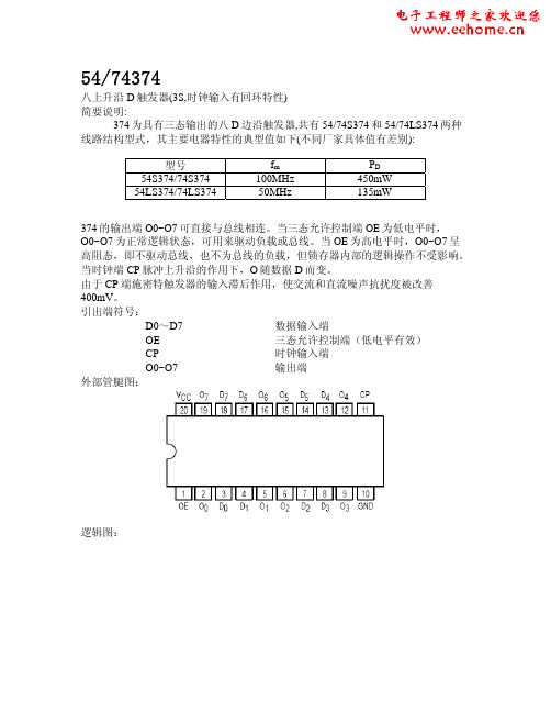
54/74374八上升沿D触发器(3S,时钟输入有回环特性)简要说明:374为具有三态输出的八D边沿触发器,共有54/74S374和54/74LS374两种线路结构型式,其主要电器特性的典型值如下(不同厂家具体值有差别):型号f m P D54S374/74S374 100MHz 450mW54LS374/74LS374 50MHz 135mW374的输出端O0~O7可直接与总线相连。
当三态允许控制端OE为低电平时,O0~O7为正常逻辑状态,可用来驱动负载或总线。
当OE为高电平时,O0~O7呈高阻态,即不驱动总线,也不为总线的负载,但锁存器内部的逻辑操作不受影响。
当时钟端CP脉冲上升沿的作用下,O随数据D而变。
由于CP端施密特触发器的输入滞后作用,使交流和直流噪声抗扰度被改善400mV。
引出端符号:D0~D7 数据输入端OE 三态允许控制端(低电平有效)CP 时钟输入端O0~O7 输出端外部管腿图:逻辑图:真值表:极限值:电源电压 (7V)输入电压5.5V54/74S374…………………………….………….7V 54/74LS374…………………………………….输出高阻态时高电平电压 …………………………. 5.5V工作环境温度54XXX ………………………………….-55~125℃0~70℃74XXX ………………………………….存储温度 …………………………………………. -65~150℃推荐工作条件:54/74374 54/74LS374单位最小额定最大最小额定最大54 4.5 5 5.5 4.5 5 5.5V 电源电压Vcc74 4.75 5 5.25 4.75 5 5.25输入高电平电压V iH 2 2 V54 0.8 0.7V输入低电平电压V iL74 0.8 0.854 -2 -1mA输出高电平电流I OH74 -6.5 -2.654 20 12mA输出低电平电流I OL74 20 24CP(H) 6 15ns脉冲宽度t wCP(L) 7.3 15保持时间t H D 2↓0↓ns建立时间t set D 5↓20↓ns静态特性(TA 为工作环境温度范围)S374 LS374 参 数 测 试 条 件【1】最小 最大 最小 最大单位V IK 输入嵌位电压 Vcc=最小,I ik =-18mA-1.5 -1.5 V V OH 输出高电平电压 Vcc =最小,V IL =最大,V IH =2V ,I OH =最大2.4 2.4 V 54 0.5 0.4 V OL 输出低电平电压 Vcc=最小,V IL =最大,V IH =2V,I OL =最大74 0.5 0.5 V V I =5.5V 1 I I 最大输入电压时输入电流Vcc =最大 V I =7V 0.1 mA V IL =0.5V -0.25 I IL 输入低电平电流 Vcc =最大, V IL =0.4V -0.4mA I IH输入高电平电流 Vcc =最大,V IH =2.7V50 20 uA I OS 输出短路电流 Vcc =最大-40 -100 -30 -130 mA Icc 电源电流 Vcc =最大,OE 接4.5V140 40 mA V 0=2.4V 50 I OZH 输出高阻态时高电平电流 Vcc =最大,V IH =2V V 0=2.7V20 mA V 0=0.5V -50 I OZL 输出高阻态时低电平电流 Vcc =最大,V IH =2V V 0=0.4V-20 mA [1]: 测试条件中的“最小”和“最大”用推荐工作条件中的相应值。
- 1、下载文档前请自行甄别文档内容的完整性,平台不提供额外的编辑、内容补充、找答案等附加服务。
- 2、"仅部分预览"的文档,不可在线预览部分如存在完整性等问题,可反馈申请退款(可完整预览的文档不适用该条件!)。
- 3、如文档侵犯您的权益,请联系客服反馈,我们会尽快为您处理(人工客服工作时间:9:00-18:30)。
General DescriptionThe MAX4173 low-cost, precision, high-side current-sense amplifier is available in a tiny SOT23-6 package.It features a voltage output that eliminates the need for gain-setting resistors and it is ideal for today’s notebook computers, cell phones, and other systems where cur-rent monitoring is critical. High-side current monitoring is especially useful in battery-powered systems, since it does not interfere with the ground path of the battery charger. The input common-mode range of 0 to +28V is independent of the supply voltage and ensures that the current-sense feedback remains viable even when con-nected to a battery in deep discharge. The MAX4173’s wide 1.7MHz bandwidth makes it suitable for use inside battery charger control loops.The combination of three gain versions and a user-selectable external sense resistor sets the full-scale current reading. This feature offers a high level of inte-gration, resulting in a simple and compact current-sense solution.The MAX4173 operates from a single +3V to +28V sup-ply, typically draws only 420µA of supply current over the extended operating temperature range (-40°C to +85°C), and is offered in the space-saving SOT23-6package.ApplicationsNotebook ComputersPortable/Battery-Powered Systems Smart Battery Packs/Chargers Cell PhonesPower-Management SystemsGeneral System/Board-Level Current Monitoring PA Bias ControlPrecision Current SourcesFeatures♦Low-Cost, Compact Current-Sense Solution ♦Wide 0 to +28V Common-Mode Range Independent of Supply Voltage ♦Three Gain Versions Available+20V/V (MAX4173T)+50V/V (MAX4173F)+100V/V (MAX4173H)♦±0.5% Full-Scale Accuracy♦±0.3mV Input Offset Voltage (MAX4173T)♦420µA Supply Current♦Wide 1.7MHz Bandwidth (MAX4173T)♦+3V to +28V Operating Supply♦Available in Space-Saving SOT23-6 PackageMAX4173T/F/HLow-Cost, SOT23, Voltage-Output, High-Side Current-Sense Amplifier________________________________________________________________Maxim Integrated Products 1Typical Operating Circuit19-1434; Rev 3; 12/04Ordering InformationPin Configurations appear at end of data sheet.For pricing, delivery, and ordering information,please contact Maxim/Dallas Direct!at 1-888-629-4642, or visit Maxim’s website at .M A X 4173T /F /HLow-Cost, SOT23, Voltage-Output, High-Side Current-Sense Amplifier 2_______________________________________________________________________________________ABSOLUTE MAXIMUM RATINGSELECTRICAL CHARACTERISTICS(V RS+ = 0 to +28V, V CC = +3V to +28V, V SENSE = 0V, T A = T MIN to T MAX , R LOAD = ∞unless otherwise noted. Typical values are at T A = +25°C.) (Note 1)Stresses beyond those listed under “Absolute Maximum Ratings” may cause permanent damage to the device. These are stress ratings only, and functional operation of the device at these or any other conditions beyond those indicated in the operational sections of the specifications is not implied. Exposure to absolute maximum rating conditions for extended periods may affect device reliability.V CC , RS+, RS- to GND..........................................-0.3V to +30V OUT to GND.............................................. -0.3V to (V CC + 0.3V)Output Short-Circuit to V CC or GND ......................... Continuous Differential Input Voltage (V RS+- V RS-).............................±0.3V Current into Any Pin.........................................................±20mAContinuous Power Dissipation (T A = +70°C)8-Pin SO (derate 5.88mW/°C above +70°C)...............471mW SOT23-6 (derate 8.7mW/°C above +70°C).................696mW Operating Temperature Range ..........................-40°C to +85°C Storage Temperature Range............................-65°C to +150°C Lead Temperature (soldering, 10s)................................+300°CMAX4173T/F/HLow-Cost, SOT23, Voltage-Output, High-Side Current-Sense Amplifier_______________________________________________________________________________________3Note 3:Total OUT Voltage Error is the sum of gain and offset voltage errors.Note 4:+6.25mV = 1/16 of +100mV full-scale voltage.Note 5:V SENSE such that output stage is in saturation.Note 6:V OS is extrapolated from the Gain Accuracy tests.Note 7:The device does not experience phase reversal when overdriven.ELECTRICAL CHARACTERISTICS (continued)(V RS+ = 0 to +28V, V CC = +3V to +28V, V SENSE = 0V, T A = T MIN to T MAX , R LOAD = ∞unless otherwise noted. Typical values are at T = +25°C.) (Note 1)M A X 4173T /F /HLow-Cost, SOT23, Voltage-Output, High-Side Current-Sense Amplifier 4_______________________________________________________________________________________370390380410400430420440010155202530SUPPLY CURRENT vs. SUPPLY VOLTAGESUPPLY VOLTAGE (V)S U P P L Y C U R R E N T (µA )200300250450400350550500150-50-510-35-202540557085SUPPLY CURRENT vs. TEMPERATURETEMPERATURE (°C)S U P P L Y C U R R E N T (µA )0.40.20.80.61.21.01.4V RS+ (V)S U P P L Y C U R R E N T (m A )-0.60-0.45-0.30-0.1500.150.300.450.60010515202530TOTAL OUTPUT ERROR vs.SUPPLY VOLTAGESUPPLY VOLTAGE (V)T O T A L O U T P U T E R R O R (%)0-1001001k10k100k1M10MPOWER-SUPPLY REJECTIONvs. FREQUENCY-80M A X 4173 t o c 07FREQUENCY (Hz)P S R (d B )-60-40-20-10-90-70-50-30-6-2-42046010155202530TOTAL OUTPUT ERROR vs. SUPPLY VOLTAGESUPPLY VOLTAGE (V)T O T A L O U T P U T E R R O R (%)-20-1213410050150200TOTAL OUTPUT ERROR vs.FULL-SCALE SENSE VOLTAGEV SENSE (mV)T O T A L O U T P U T E R R O R (%)-10-8-6-4-2024610515202530TOTAL OUTPUT ERROR MON-MODE VOLTAGECOMMON-MODE VOLTAGE (V)T O T A L O U T P U T E R R O R (%)Typical Operating Characteristics(V CC = +12V, V RS+= +12V, V SENSE = +100mV, TA = +25°C, unless otherwise noted.)-1.2-0.4-0.800.40.81.2-50-20-510-352540557085GAIN ACCURACY vs. TEMPERATURETEMPERATURE (°C)G A I N A C C U R A C Y (%)MAX4173T/F/HLow-Cost, SOT23, Voltage-Output, High-Side Current-Sense Amplifier_______________________________________________________________________________________5Typical Operating Characteristics (continued)(V CC = +12V, V RS+= +12V, V SENSE = +100mV, T A = +25°C, unless otherwise noted.)-2.0-1.0-1.50.50-0.51.51.02.0-50-510-35-202540557085TOTAL OUTPUT ERROR vs. TEMPERATURETEMPERATURE (°C)T O T A L O U T P U T E R R O R (%)2µs/divMAX4173TLARGE-SIGNAL TRANSIENT RESPONSE(V SENSE = 6mV to 100mV)IN(45mV/div)OUT (500mV/div)6mV 100mV 2V0.120VC L = 5pF2µs/div MAX4173FLARGE-SIGNAL TRANSIENT RESPONSE(V SENSE = 6mV to 100mV)IN(45mV/div)OUT (2V/div)6mV100mV 5V0.3VC L = 5pF2µs/divMAX4173HLARGE-SIGNAL TRANSIENT RESPONSE(V SENSE = 6mV to 100mV)IN(45mV/div)OUT (3V/div)6mV 100mV10V0.6VC L = 5pF2µs/divMAX4173TSMALL-SIGNAL TRANSIENT RESPONSE(V SENSE = 95mV TO 100mV)IN (5mV/div)OUT (50mV/div)95mV100mV 2.0V1.9VC L = 5pF2µs/divMAX4173FSMALL-SIGNAL TRANSIENT RESPONSE(V SENSE = 95mV TO 100mV)IN (5mV/div)OUT (100mV/div)95mV100mV 5V4.75VC L = 5pFM A X 4173T /F /HLow-Cost, SOT23, Voltage-Output, High-Side Current-Sense Amplifier 6_______________________________________________________________________________________Pin DescriptionTypical Operating Characteristics (continued)(V CC = +12V, V RS+= +12V, V SENSE = +100mV, T A = +25°C, unless otherwise noted.)2µs/divMAX4173HSMALL-SIGNAL TRANSIENT RESPONSE(V SENSE = 95mV to 100mV)IN (5mV/div)OUT (200mV/div)95mV100mV 10V9.5VC L = 5pF5µs/divSTART-UP DELAY (V CC = 0 to 4V)(V SENSE = 100mV)IN (2V/div)OUT (1V/div)0V4V2V0VM A X 4173 t o c 17MAX4173T/F/HLow-Cost, SOT23, Voltage-Output, High-Side Current-Sense Amplifier_______________________________________________________________________________________7Detailed DescriptionThe MAX4173 high-side current-sense amplifier fea-tures a 0 to +28V input common-mode range that is independent of supply voltage. This feature allows the monitoring of current out of a battery in deep discharge and also enables high-side current sensing at voltages greater than the supply voltage (V CC ).The MAX4173 operates as follows:Current from the source flows through R SENSE to the load (Figure 1). Since the internal-sense amplifier’s inverting input has high impedance, negligible current flows through RG2(neglecting the input bias current). Therefore, the sense amplifier’s inverting-input voltage equals V SOURCE - (I LOAD )(R SENSE ). The amplifier’s open-loop gain forces its noninverting input to the same voltage as the inverting input. Therefore, the drop across RG1equals (I LOAD )(R SENSE ). Since I RG1flows through RG1,I RG1= (I LOAD )(R SENSE ) / RG1. The internal current mirror multiplies I RG1by a current gain factor, β, to give I RGD = β·I RG1. Solving I RGD = β·(I LOAD )(R SENSE ) /RG1. Assuming infinite output impedance, V OUT = (I RGD )(RGD). Substituting in for I RGD and rearranging, V OUT = β·(RGD / RG1)(R SENSE ·I LOAD ). The parts gain equals β·RGD / RG1. Therefore, V OUT = (GAI N) (R SENSE )(I LOAD ), where GAIN = 20 for MAX4173T, GAIN = 50 for MAX4173F, and GAIN = 100 for MAX4173H.Set the full-scale output range by selecting R SENSE and the appropriate gain version of the MAX4173.Applications InformationRecommended Component ValuesThe MAX4173 senses a wide variety of currents with different sense resistor values. Table 1 lists common resistor values for typical operation of the MAX4173.Choosing R SENSETo measure lower currents more accurately, use a high value for R SENSE . The high value develops a higher sense voltage that reduces offset voltage errors of the internal op amp.I n applications monitoring very high currents, R SENSE must be able to dissipate the I 2R losses. If the resistor’s rated power dissipation is exceeded, its value may drift or it may fail altogether, causing a differential voltage across the terminals in excess of the absolute maxi-mum ratings.If I SENSE has a large high-frequency component, mini-mize the inductance of R SENSE . Wire-wound resistors have the highest inductance, metal-film resistors are somewhat better, and low-inductance metal-film resis-tors are best suited for these applications.Using a PCB Trace as R SENSEI f the cost of R SENSE is an issue and accuracy is not critical, use the alternative solution shown in Figure 2.This solution uses copper PC board traces to create a sense resistor. The resistivity of a 0.1-inch-wide trace of 2-ounce copper is approximately 30m Ω/ft. The resis-tance-temperature coefficient of copper is fairly high (approximately 0.4%/°C), so systems that experience a wide temperature variance must compensate for this effect. In addition, do not exceed the maximum power dissipation of the copper trace.For example, the MAX4173T (with a maximum load cur-rent of 10A and an R SENSE of 5m Ω) creates a full-scale V SENSE of 50mV that yields a maximum V OUT of 1V.R SENSE in this case requires about 2 inches of 0.1 inch-wide copper trace.Output ImpedanceThe output of the MAX4173 is a current source driving a 12k Ωresistance. Resistive loading added to OUT reduces the output gain of the MAX4173. To minimize output errors for most applications, connect OUT to a high-impedance input stage. When output buffering is required, choose an op amp with a common-mode input range and an output voltage swing that includes ground when operating with a single supply. The opFigure 1. Functional DiagramM A X 4173T /F /HLow-Cost, SOT23, Voltage-Output, High-Side Current-Sense Amplifier 8_______________________________________________________________________________________amp’s supply voltage range should be at least as high as any voltage the system may encounter.The percent error introduced by output loading iswhere R LOAD is the external load applied to OUT.Current Source CircuitFigure 3 shows a block diagram using the MAX4173with a switching regulator to make a current source.Figure 2. MAX4173 Connections Showing Use of PC Board Figure 3. Current SourceMAX4173T/F/HLow-Cost, SOT23, Voltage-Output, High-Side Current-Sense Amplifier_______________________________________________________________________________________9Pin ConfigurationsChip InformationTRANSISTOR COUNT: 187M A X 4173T /F /HLow-Cost, SOT23, Voltage-Output, High-Side Current-Sense Amplifier 10______________________________________________________________________________________Package Information(The package drawing(s) in this data sheet may not reflect the most current specifications. For the latest package outline information,go to /packages .)Low-Cost, SOT23, Voltage-Output, High-Side Current-Sense AmplifierMAX4173T/F/H Maxim cannot assume re sponsibility for use of any circuitry othe r than circuitry e ntire ly e mbodie d in a Maxim product. No circuit pate nt lice nse s are implied. Maxim reserves the right to change the circuitry and specifications without notice at any time.Maxim Integrated Products, 120 San Gabriel Drive, Sunnyvale, CA 94086 408-737-7600____________________11©2004 Maxim Integrated Products Printed USA is a registered trademark of Maxim Integrated Products.Package Information (continued)(The package drawing(s) in this data sheet may not reflect the most current specifications. For the latest package outline information,go to /packages .)元器件交易网。