MAX483EESA+T中文资料
MAX483ESA+T中文资料
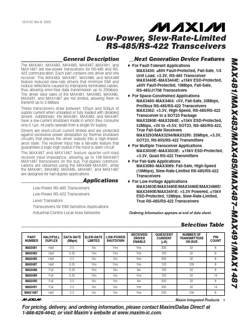
For pricing, delivery, and ordering information,please contact Maxim/Dallas Direct!at 1-888-629-4642, or visit Maxim’s website at .General DescriptionThe MAX481, MAX483, MAX485, MAX487–MAX491, and MAX1487 are low-power transceivers for RS-485 and RS-422 communication. Each part contains one driver and one receiver. The MAX483, MAX487, MAX488, and MAX489feature reduced slew-rate drivers that minimize EMI and reduce reflections caused by improperly terminated cables,thus allowing error-free data transmission up to 250kbps.The driver slew rates of the MAX481, MAX485, MAX490,MAX491, and MAX1487 are not limited, allowing them to transmit up to 2.5Mbps.These transceivers draw between 120µA and 500µA of supply current when unloaded or fully loaded with disabled drivers. Additionally, the MAX481, MAX483, and MAX487have a low-current shutdown mode in which they consume only 0.1µA. All parts operate from a single 5V supply.Drivers are short-circuit current limited and are protected against excessive power dissipation by thermal shutdown circuitry that places the driver outputs into a high-imped-ance state. The receiver input has a fail-safe feature that guarantees a logic-high output if the input is open circuit.The MAX487 and MAX1487 feature quarter-unit-load receiver input impedance, allowing up to 128 MAX487/MAX1487 transceivers on the bus. Full-duplex communi-cations are obtained using the MAX488–MAX491, while the MAX481, MAX483, MAX485, MAX487, and MAX1487are designed for half-duplex applications.________________________ApplicationsLow-Power RS-485 Transceivers Low-Power RS-422 Transceivers Level TranslatorsTransceivers for EMI-Sensitive Applications Industrial-Control Local Area Networks__Next Generation Device Features♦For Fault-Tolerant ApplicationsMAX3430: ±80V Fault-Protected, Fail-Safe, 1/4Unit Load, +3.3V, RS-485 TransceiverMAX3440E–MAX3444E: ±15kV ESD-Protected,±60V Fault-Protected, 10Mbps, Fail-Safe, RS-485/J1708 Transceivers♦For Space-Constrained ApplicationsMAX3460–MAX3464: +5V, Fail-Safe, 20Mbps,Profibus RS-485/RS-422 TransceiversMAX3362: +3.3V, High-Speed, RS-485/RS-422Transceiver in a SOT23 PackageMAX3280E–MAX3284E: ±15kV ESD-Protected,52Mbps, +3V to +5.5V, SOT23, RS-485/RS-422,True Fail-Safe ReceiversMAX3293/MAX3294/MAX3295: 20Mbps, +3.3V,SOT23, RS-855/RS-422 Transmitters ♦For Multiple Transceiver ApplicationsMAX3030E–MAX3033E: ±15kV ESD-Protected,+3.3V, Quad RS-422 Transmitters ♦For Fail-Safe ApplicationsMAX3080–MAX3089: Fail-Safe, High-Speed (10Mbps), Slew-Rate-Limited RS-485/RS-422Transceivers♦For Low-Voltage ApplicationsMAX3483E/MAX3485E/MAX3486E/MAX3488E/MAX3490E/MAX3491E: +3.3V Powered, ±15kV ESD-Protected, 12Mbps, Slew-Rate-Limited,True RS-485/RS-422 TransceiversMAX481/MAX483/MAX485/MAX487–MAX491/MAX1487Low-Power, Slew-Rate-Limited RS-485/RS-422 Transceivers______________________________________________________________Selection Table19-0122; Rev 8; 10/03Ordering Information appears at end of data sheet.M A X 481/M A X 483/M A X 485/M A X 487–M A X 491/M A X 1487Low-Power, Slew-Rate-Limited RS-485/RS-422 Transceivers 2_______________________________________________________________________________________ABSOLUTE MAXIMUM RATINGSSupply Voltage (V CC ).............................................................12V Control Input Voltage (RE , DE)...................-0.5V to (V CC + 0.5V)Driver Input Voltage (DI).............................-0.5V to (V CC + 0.5V)Driver Output Voltage (A, B)...................................-8V to +12.5V Receiver Input Voltage (A, B).................................-8V to +12.5V Receiver Output Voltage (RO).....................-0.5V to (V CC +0.5V)Continuous Power Dissipation (T A = +70°C)8-Pin Plastic DIP (derate 9.09mW/°C above +70°C)....727mW 14-Pin Plastic DIP (derate 10.00mW/°C above +70°C)..800mW 8-Pin SO (derate 5.88mW/°C above +70°C).................471mW14-Pin SO (derate 8.33mW/°C above +70°C)...............667mW 8-Pin µMAX (derate 4.1mW/°C above +70°C)..............830mW 8-Pin CERDIP (derate 8.00mW/°C above +70°C).........640mW 14-Pin CERDIP (derate 9.09mW/°C above +70°C).......727mW Operating Temperature RangesMAX4_ _C_ _/MAX1487C_ A...............................0°C to +70°C MAX4__E_ _/MAX1487E_ A.............................-40°C to +85°C MAX4__MJ_/MAX1487MJA...........................-55°C to +125°C Storage Temperature Range.............................-65°C to +160°C Lead Temperature (soldering, 10sec).............................+300°CDC ELECTRICAL CHARACTERISTICS(V CC = 5V ±5%, T A = T MIN to T MAX , unless otherwise noted.) (Notes 1, 2)Stresses beyond those listed under “Absolute Maximum Ratings” may cause permanent damage to the device. These are stress ratings only, and functional operation of the device at these or any other conditions beyond those indicated in the operational sections of the specifications is not implied. Exposure to absolute maximum rating conditions for extended periods may affect device reliability.V V IN = -7VV IN = 12V V IN = -7V V IN = 12V Input Current (A, B)I IN2V TH k Ω48-7V ≤V CM ≤12V, MAX487/MAX1487R INReceiver Input Resistance -7V ≤V CM ≤12V, all devices except MAX487/MAX1487R = 27Ω(RS-485), Figure 40.4V ≤V O ≤2.4VR = 50Ω(RS-422)I O = 4mA, V ID = -200mV I O = -4mA, V ID = 200mV V CM = 0V-7V ≤V CM ≤12V DE, DI, RE DE, DI, RE MAX487/MAX1487,DE = 0V, V CC = 0V or 5.25VDE, DI, RE R = 27Ωor 50Ω, Figure 4R = 27Ωor 50Ω, Figure 4R = 27Ωor 50Ω, Figure 4DE = 0V;V CC = 0V or 5.25V,all devices except MAX487/MAX1487CONDITIONSk Ω12µA ±1I OZRThree-State (high impedance)Output Current at ReceiverV 0.4V OL Receiver Output Low Voltage 3.5V OH Receiver Output High Voltage mV 70∆V TH Receiver Input Hysteresis V -0.20.2Receiver Differential Threshold Voltage-0.2mA 0.25mA-0.81.01.55V OD2Differential Driver Output (with load)V 2V 5V OD1Differential Driver Output (no load)µA±2I IN1Input CurrentV 0.8V IL Input Low Voltage V 2.0V IH Input High Voltage V 0.2∆V OD Change in Magnitude of Driver Common-Mode Output Voltage for Complementary Output States V 0.2∆V OD Change in Magnitude of Driver Differential Output Voltage for Complementary Output States V 3V OC Driver Common-Mode Output VoltageUNITS MINTYPMAX SYMBOL PARAMETERMAX481/MAX483/MAX485/MAX487–MAX491/MAX1487Low-Power, Slew-Rate-Limited RS-485/RS-422 Transceivers_______________________________________________________________________________________3SWITCHING CHARACTERISTICS—MAX481/MAX485, MAX490/MAX491, MAX1487(V CC = 5V ±5%, T A = T MIN to T MAX , unless otherwise noted.) (Notes 1, 2)DC ELECTRICAL CHARACTERISTICS (continued)(V CC = 5V ±5%, T A = T MIN to T MAX , unless otherwise noted.) (Notes 1, 2)ns 103060t PHLDriver Rise or Fall Time Figures 6 and 8, R DIFF = 54Ω, C L1= C L2= 100pF ns MAX490M, MAX491M MAX490C/E, MAX491C/E2090150MAX481, MAX485, MAX1487MAX490M, MAX491MMAX490C/E, MAX491C/E MAX481, MAX485, MAX1487Figures 6 and 8, R DIFF = 54Ω,C L1= C L2= 100pF MAX481 (Note 5)Figures 5 and 11, C RL = 15pF, S2 closedFigures 5 and 11, C RL = 15pF, S1 closed Figures 5 and 11, C RL = 15pF, S2 closed Figures 5 and 11, C RL = 15pF, S1 closed Figures 6 and 10, R DIFF = 54Ω,C L1= C L2= 100pFFigures 6 and 8,R DIFF = 54Ω,C L1= C L2= 100pF Figures 6 and 10,R DIFF = 54Ω,C L1= C L2= 100pF CONDITIONS ns 510t SKEW ns50200600t SHDNTime to ShutdownMbps 2.5f MAX Maximum Data Rate ns 2050t HZ Receiver Disable Time from High ns 103060t PLH 2050t LZ Receiver Disable Time from Low ns 2050t ZH Driver Input to Output Receiver Enable to Output High ns 2050t ZL Receiver Enable to Output Low 2090200ns ns 134070t HZ t SKD Driver Disable Time from High |t PLH - t PHL |DifferentialReceiver Skewns 4070t LZ Driver Disable Time from Low ns 4070t ZL Driver Enable to Output Low 31540ns51525ns 31540t R , t F 2090200Driver Output Skew to Output t PLH , t PHL Receiver Input to Output4070t ZH Driver Enable to Output High UNITS MIN TYP MAX SYMBOL PARAMETERFigures 7 and 9, C L = 100pF, S2 closed Figures 7 and 9, C L = 100pF, S1 closed Figures 7 and 9, C L = 15pF, S1 closed Figures 7 and 9, C L = 15pF, S2 closedM A X 481/M A X 483/M A X 485/M A X 487–M A X 491/M A X 1487Low-Power, Slew-Rate-Limited RS-485/RS-422 Transceivers 4_______________________________________________________________________________________SWITCHING CHARACTERISTICS—MAX483, MAX487/MAX488/MAX489(V CC = 5V ±5%, T A = T MIN to T MAX , unless otherwise noted.) (Notes 1, 2)SWITCHING CHARACTERISTICS—MAX481/MAX485, MAX490/MAX491, MAX1487 (continued)(V CC = 5V ±5%, T A = T MIN to T MAX , unless otherwise noted.) (Notes 1, 2)3001000Figures 7 and 9, C L = 100pF, S2 closed Figures 7 and 9, C L = 100pF, S1 closed Figures 5 and 11, C L = 15pF, S2 closed,A - B = 2VCONDITIONSns 40100t ZH(SHDN)Driver Enable from Shutdown toOutput High (MAX481)nsFigures 5 and 11, C L = 15pF, S1 closed,B - A = 2Vt ZL(SHDN)Receiver Enable from Shutdownto Output Low (MAX481)ns 40100t ZL(SHDN)Driver Enable from Shutdown toOutput Low (MAX481)ns 3001000t ZH(SHDN)Receiver Enable from Shutdownto Output High (MAX481)UNITS MINTYP MAX SYMBOLPARAMETERt PLH t SKEW Figures 6 and 8, R DIFF = 54Ω,C L1= C L2= 100pFt PHL Figures 6 and 8, R DIFF = 54Ω,C L1= C L2= 100pFDriver Input to Output Driver Output Skew to Output ns 100800ns ns 2000MAX483/MAX487, Figures 7 and 9,C L = 100pF, S2 closedt ZH(SHDN)Driver Enable from Shutdown to Output High2502000ns2500MAX483/MAX487, Figures 5 and 11,C L = 15pF, S1 closedt ZL(SHDN)Receiver Enable from Shutdown to Output Lowns 2500MAX483/MAX487, Figures 5 and 11,C L = 15pF, S2 closedt ZH(SHDN)Receiver Enable from Shutdown to Output Highns 2000MAX483/MAX487, Figures 7 and 9,C L = 100pF, S1 closedt ZL(SHDN)Driver Enable from Shutdown to Output Lowns 50200600MAX483/MAX487 (Note 5) t SHDN Time to Shutdownt PHL t PLH , t PHL < 50% of data period Figures 5 and 11, C RL = 15pF, S2 closed Figures 5 and 11, C RL = 15pF, S1 closed Figures 5 and 11, C RL = 15pF, S2 closed Figures 5 and 11, C RL = 15pF, S1 closed Figures 7 and 9, C L = 15pF, S2 closed Figures 6 and 10, R DIFF = 54Ω,C L1= C L2= 100pFFigures 7 and 9, C L = 15pF, S1 closed Figures 7 and 9, C L = 100pF, S1 closed Figures 7 and 9, C L = 100pF, S2 closed CONDITIONSkbps 250f MAX 2508002000Maximum Data Rate ns 2050t HZ Receiver Disable Time from High ns 25080020002050t LZ Receiver Disable Time from Low ns 2050t ZH Receiver Enable to Output High ns 2050t ZL Receiver Enable to Output Low ns ns 1003003000t HZ t SKD Driver Disable Time from High I t PLH - t PHL I DifferentialReceiver SkewFigures 6 and 10, R DIFF = 54Ω,C L1= C L2= 100pFns 3003000t LZ Driver Disable Time from Low ns 2502000t ZL Driver Enable to Output Low ns Figures 6 and 8, R DIFF = 54Ω,C L1= C L2= 100pFns 2502000t R , t F 2502000Driver Rise or Fall Time ns t PLH Receiver Input to Output2502000t ZH Driver Enable to Output High UNITS MIN TYP MAX SYMBOL PARAMETERMAX481/MAX483/MAX485/MAX487–MAX491/MAX1487Low-Power, Slew-Rate-Limited RS-485/RS-422 Transceivers_______________________________________________________________________________________530002.5OUTPUT CURRENT vs.RECEIVER OUTPUT LOW VOLTAGE525M A X 481-01OUTPUT LOW VOLTAGE (V)O U T P U T C U R R E N T (m A )1.515100.51.02.0203540450.90.1-50-252575RECEIVER OUTPUT LOW VOLTAGE vs.TEMPERATURE0.30.7TEMPERATURE (°C)O U T P U TL O W V O L T A G E (V )500.50.80.20.60.40100125-20-41.5 2.0 3.0 5.0OUTPUT CURRENT vs.RECEIVER OUTPUT HIGH VOLTAGE-8-16M A X 481-02OUTPUT HIGH VOLTAGE (V)O U T P U T C U R R E N T (m A )2.5 4.0-12-18-6-14-10-203.54.5 4.83.2-50-252575RECEIVER OUTPUT HIGH VOLTAGE vs.TEMPERATURE3.64.4TEMPERATURE (°C)O U T P UT H I G H V O L T A G E (V )0504.04.63.44.23.83.01001259000 1.0 3.0 4.5DRIVER OUTPUT CURRENT vs.DIFFERENTIAL OUTPUT VOLTAGE1070M A X 481-05DIFFERENTIAL OUTPUT VOLTAGE (V)O U T P U T C U R R E N T (m A )2.0 4.05030806040200.5 1.5 2.53.5 2.31.5-50-2525125DRIVER DIFFERENTIAL OUTPUT VOLTAGEvs. TEMPERATURE1.72.1TEMPERATURE (°C)D I F FE R E N T I A L O U T P U T V O L T A G E (V )751.92.21.62.01.8100502.4__________________________________________Typical Operating Characteristics(V CC = 5V, T A = +25°C, unless otherwise noted.)NOTES FOR ELECTRICAL/SWITCHING CHARACTERISTICSNote 1:All currents into device pins are positive; all currents out of device pins are negative. All voltages are referenced to deviceground unless otherwise specified.Note 2:All typical specifications are given for V CC = 5V and T A = +25°C.Note 3:Supply current specification is valid for loaded transmitters when DE = 0V.Note 4:Applies to peak current. See Typical Operating Characteristics.Note 5:The MAX481/MAX483/MAX487 are put into shutdown by bringing RE high and DE low. If the inputs are in this state for lessthan 50ns, the parts are guaranteed not to enter shutdown. If the inputs are in this state for at least 600ns, the parts are guaranteed to have entered shutdown. See Low-Power Shutdown Mode section.M A X 481/M A X 483/M A X 485/M A X 487–M A X 491/M A X 1487Low-Power, Slew-Rate-Limited RS-485/RS-422 Transceivers 6___________________________________________________________________________________________________________________Typical Operating Characteristics (continued)(V CC = 5V, T A = +25°C, unless otherwise noted.)120008OUTPUT CURRENT vs.DRIVER OUTPUT LOW VOLTAGE20100M A X 481-07OUTPUT LOW VOLTAGE (V)O U T P U T C U R R E N T (m A )6604024801012140-1200-7-5-15OUTPUT CURRENT vs.DRIVER OUTPUT HIGH VOLTAGE-20-80M A X 481-08OUTPUT HIGH VOLTAGE (V)O U T P U T C U R R E N T (m A )-31-603-6-4-2024-100-40100-40-60-2040100120MAX1487SUPPLY CURRENT vs. TEMPERATURE300TEMPERATURE (°C)S U P P L Y C U R R E N T (µA )20608050020060040000140100-50-2550100MAX481/MAX485/MAX490/MAX491SUPPLY CURRENT vs. TEMPERATURE300TEMPERATURE (°C)S U P P L Y C U R R E N T (µA )257550020060040000125100-50-2550100MAX483/MAX487–MAX489SUPPLY CURRENT vs. TEMPERATURE300TEMPERATURE (°C)S U P P L Y C U R R E N T (µA )257550020060040000125MAX481/MAX483/MAX485/MAX487–MAX491/MAX1487Low-Power, Slew-Rate-Limited RS-485/RS-422 Transceivers_______________________________________________________________________________________7______________________________________________________________Pin DescriptionFigure 1. MAX481/MAX483/MAX485/MAX487/MAX1487 Pin Configuration and Typical Operating CircuitM A X 481/M A X 483/M A X 485/M A X 487–M A X 491/M A X 1487__________Applications InformationThe MAX481/MAX483/MAX485/MAX487–MAX491 and MAX1487 are low-power transceivers for RS-485 and RS-422 communications. The MAX481, MAX485, MAX490,MAX491, and MAX1487 can transmit and receive at data rates up to 2.5Mbps, while the MAX483, MAX487,MAX488, and MAX489 are specified for data rates up to 250kbps. The MAX488–MAX491 are full-duplex trans-ceivers while the MAX481, MAX483, MAX485, MAX487,and MAX1487 are half-duplex. In addition, Driver Enable (DE) and Receiver Enable (RE) pins are included on the MAX481, MAX483, MAX485, MAX487, MAX489,MAX491, and MAX1487. When disabled, the driver and receiver outputs are high impedance.MAX487/MAX1487:128 Transceivers on the BusThe 48k Ω, 1/4-unit-load receiver input impedance of the MAX487 and MAX1487 allows up to 128 transceivers on a bus, compared to the 1-unit load (12k Ωinput impedance) of standard RS-485 drivers (32 trans-ceivers maximum). Any combination of MAX487/MAX1487 and other RS-485 transceivers with a total of 32 unit loads or less can be put on the bus. The MAX481/MAX483/MAX485 and MAX488–MAX491 have standard 12k ΩReceiver Input impedance.Low-Power, Slew-Rate-Limited RS-485/RS-422 Transceivers 8_______________________________________________________________________________________Figure 2. MAX488/MAX490 Pin Configuration and Typical Operating CircuitFigure 3. MAX489/MAX491 Pin Configuration and Typical Operating CircuitMAX483/MAX487/MAX488/MAX489:Reduced EMI and ReflectionsThe MAX483 and MAX487–MAX489 are slew-rate limit-ed, minimizing EMI and reducing reflections caused by improperly terminated cables. Figure 12 shows the dri-ver output waveform and its Fourier analysis of a 150kHz signal transmitted by a MAX481, MAX485,MAX490, MAX491, or MAX1487. High-frequency har-monics with large amplitudes are evident. Figure 13shows the same information displayed for a MAX483,MAX487, MAX488, or MAX489 transmitting under the same conditions. Figure 13’s high-frequency harmonics have much lower amplitudes, and the potential for EMI is significantly reduced.MAX481/MAX483/MAX485/MAX487–MAX491/MAX1487Low-Power, Slew-Rate-Limited RS-485/RS-422 Transceivers_______________________________________________________________________________________9_________________________________________________________________Test CircuitsFigure 4. Driver DC Test Load Figure 5. Receiver Timing Test LoadFigure 6. Driver/Receiver Timing Test Circuit Figure 7. Driver Timing Test LoadM A X 481/M A X 483/M A X 485/M A X 487–M A X 491/M A X 1487Low-Power, Slew-Rate-Limited RS-485/RS-422 Transceivers 10_______________________________________________________Switching Waveforms_________________Function Tables (MAX481/MAX483/MAX485/MAX487/MAX1487)Figure 8. Driver Propagation DelaysFigure 9. Driver Enable and Disable Times (except MAX488 and MAX490)Figure 10. Receiver Propagation DelaysFigure 11. Receiver Enable and Disable Times (except MAX488and MAX490)Table 1. TransmittingTable 2. ReceivingLow-Power Shutdown Mode (MAX481/MAX483/MAX487)A low-power shutdown mode is initiated by bringing both RE high and DE low. The devices will not shut down unless both the driver and receiver are disabled.In shutdown, the devices typically draw only 0.1µA of supply current.RE and DE may be driven simultaneously; the parts are guaranteed not to enter shutdown if RE is high and DE is low for less than 50ns. If the inputs are in this state for at least 600ns, the parts are guaranteed to enter shutdown.For the MAX481, MAX483, and MAX487, the t ZH and t ZL enable times assume the part was not in the low-power shutdown state (the MAX485/MAX488–MAX491and MAX1487 can not be shut down). The t ZH(SHDN)and t ZL(SHDN)enable times assume the parts were shut down (see Electrical Characteristics ).It takes the drivers and receivers longer to become enabled from the low-power shutdown state (t ZH(SHDN ), t ZL(SHDN)) than from the operating mode (t ZH , t ZL ). (The parts are in operating mode if the –R —E –,DE inputs equal a logical 0,1 or 1,1 or 0, 0.)Driver Output ProtectionExcessive output current and power dissipation caused by faults or by bus contention are prevented by two mechanisms. A foldback current limit on the output stage provides immediate protection against short cir-cuits over the whole common-mode voltage range (see Typical Operating Characteristics ). In addition, a ther-mal shutdown circuit forces the driver outputs into a high-impedance state if the die temperature rises excessively.Propagation DelayMany digital encoding schemes depend on the differ-ence between the driver and receiver propagation delay times. Typical propagation delays are shown in Figures 15–18 using Figure 14’s test circuit.The difference in receiver delay times, | t PLH - t PHL |, is typically under 13ns for the MAX481, MAX485,MAX490, MAX491, and MAX1487 and is typically less than 100ns for the MAX483 and MAX487–MAX489.The driver skew times are typically 5ns (10ns max) for the MAX481, MAX485, MAX490, MAX491, and MAX1487, and are typically 100ns (800ns max) for the MAX483 and MAX487–MAX489.MAX481/MAX483/MAX485/MAX487–MAX491/MAX1487Low-Power, Slew-Rate-Limited RS-485/RS-422 Transceivers______________________________________________________________________________________1110dB/div0Hz5MHz500kHz/div10dB/div0Hz5MHz500kHz/divFigure 12. Driver Output Waveform and FFT Plot of MAX481/MAX485/MAX490/MAX491/MAX1487 Transmitting a 150kHz SignalFigure 13. Driver Output Waveform and FFT Plot of MAX483/MAX487–MAX489 Transmitting a 150kHz SignalM A X 481/M A X 483/M A X 485/M A X 487–M A X 491/M A X 1487Low-Power, Slew-Rate-Limited RS-485/RS-422 Transceivers 12______________________________________________________________________________________V CC = 5V T A = +25°CV CC = 5V T A = +25°CV CC = 5V T A = +25°CV CC = 5V T A = +25°CFigure 14. Receiver Propagation Delay Test CircuitFigure 15. MAX481/MAX485/MAX490/MAX491/MAX1487Receiver t PHLFigure 16. MAX481/MAX485/MAX490/MAX491/MAX1487Receiver t PLHPHL Figure 18. MAX483, MAX487–MAX489 Receiver t PLHLine Length vs. Data RateThe RS-485/RS-422 standard covers line lengths up to 4000 feet. For line lengths greater than 4000 feet, see Figure 23.Figures 19 and 20 show the system differential voltage for the parts driving 4000 feet of 26AWG twisted-pair wire at 110kHz into 120Ωloads.Typical ApplicationsThe MAX481, MAX483, MAX485, MAX487–MAX491, and MAX1487 transceivers are designed for bidirectional data communications on multipoint bus transmission lines.Figures 21 and 22 show typical network applications circuits. These parts can also be used as line repeaters, with cable lengths longer than 4000 feet, as shown in Figure 23.To minimize reflections, the line should be terminated at both ends in its characteristic impedance, and stub lengths off the main line should be kept as short as possi-ble. The slew-rate-limited MAX483 and MAX487–MAX489are more tolerant of imperfect termination.MAX481/MAX483/MAX485/MAX487–MAX491/MAX1487Low-Power, Slew-Rate-Limited RS-485/RS-422 Transceivers______________________________________________________________________________________13DIV Y -V ZRO5V 0V1V0V -1V5V 0V2µs/divFigure 19. MAX481/MAX485/MAX490/MAX491/MAX1487 System Differential Voltage at 110kHz Driving 4000ft of Cable Figure 20. MAX483, MAX487–MAX489 System Differential Voltage at 110kHz Driving 4000ft of CableFigure 21. MAX481/MAX483/MAX485/MAX487/MAX1487 Typical Half-Duplex RS-485 NetworkM A X 481/M A X 483/M A X 485/M A X 487–M A X 491/M A X 1487Low-Power, Slew-Rate-Limited RS-485/RS-422 Transceivers 14______________________________________________________________________________________Figure 22. MAX488–MAX491 Full-Duplex RS-485 NetworkFigure 23. Line Repeater for MAX488–MAX491Isolated RS-485For isolated RS-485 applications, see the MAX253 and MAX1480 data sheets.MAX481/MAX483/MAX485/MAX487–MAX491/MAX1487Low-Power, Slew-Rate-Limited RS-485/RS-422 Transceivers______________________________________________________________________________________15_______________Ordering Information_________________Chip TopographiesMAX481/MAX483/MAX485/MAX487/MAX1487N.C. RO 0.054"(1.372mm)0.080"(2.032mm)DE DIGND B N.C.V CCARE * Contact factory for dice specifications.__Ordering Information (continued)M A X 481/M A X 483/M A X 485/M A X 487–M A X 491/M A X 1487Low-Power, Slew-Rate-Limited RS-485/RS-422 Transceivers 16______________________________________________________________________________________TRANSISTOR COUNT: 248SUBSTRATE CONNECTED TO GNDMAX488/MAX490B RO 0.054"(1.372mm)0.080"(2.032mm)N.C. DIGND Z A V CCYN.C._____________________________________________Chip Topographies (continued)MAX489/MAX491B RO 0.054"(1.372mm)0.080"(2.032mm)DE DIGND Z A V CCYREMAX481/MAX483/MAX485/MAX487–MAX491/MAX1487Low-Power, Slew-Rate-Limited RS-485/RS-422 Transceivers______________________________________________________________________________________17Package Information(The package drawing(s) in this data sheet may not reflect the most current specifications. For the latest package outline information go to /packages .)S O I C N .E P SM A X 481/M A X 483/M A X 485/M A X 487–M A X 491/M A X 1487Low-Power, Slew-Rate-Limited RS-485/RS-422 Transceivers 18______________________________________________________________________________________Package Information (continued)(The package drawing(s) in this data sheet may not reflect the most current specifications. For the latest package outline information go to /packages .)MAX481/MAX483/MAX485/MAX487–MAX491Low-Power, Slew-Rate-Limited RS-485/RS-422 TransceiversMaxim cannot assume responsibility for use of any circuitry other than circuitry entirely embodied in a Maxim product. No circuit patent licenses are implied. Maxim reserves the right to change the circuitry and specifications without notice at any time.Maxim Integrated Products, 120 San Gabriel Drive, Sunnyvale, CA 94086 408-737-7600 ____________________19©2003 Maxim Integrated ProductsPrinted USAis a registered trademark of Maxim Integrated Products.M A X 481/M A X 483/M A X 485/M A X 487–M A X 491/M A X 1487P D I P N .E PSPackage Information (continued)(The package drawing(s) in this data sheet may not reflect the most current specifications. For the latest package outline information go to /packages .)。
MAX491EESD+中文资料

Driver Input Voltage (DI).............................-0.5V to (VCC + 0.5V)
Driver Output Voltage (Y, Z; A, B) ..........................-8V to +12.5V
Receiver Input Voltage (A, B).................................-8V to +12.5V
元器件交易网
MAX481E/MAX483E/MAX485E/MAX487E–MAX491E/MAX1487E
±15kV ESD-Protected, Slew-Rate-Limited, Low-Power, RS-485/RS-422 Transceivers
ABSOLUTE MAXIMUM RATINGS
General Description
The MAX481E, MAX483E, MAX485E, MAX487E– MAX491E, and MAX1487E are low-power transceivers for RS-485 and RS-422 communications in harsh environments. Each driver output and receiver input is protected against ±15kV electro-static discharge (ESD) shocks, without latchup. These parts contain one driver and one receiver. The MAX483E, MAX487E, MAX488E, and MAX489E feature reduced slew-rate drivers that minimize EMI and reduce reflections caused by improperly terminated cables, thus allowing error-free data transmission up to 250kbps. The driver slew rates of the MAX481E, MAX485E, MAX490E, MAX491E, and MAX1487E are not limited, allowing them to transmit up to 2.5Mbps.
MAX202EEWE+T中文资料
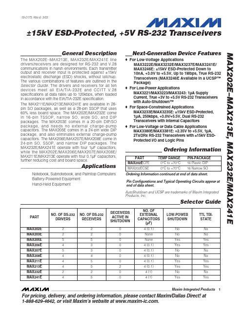
________________________________________________________________Maxim Integrated Products 1General DescriptionThe MAX202E–MAX213E, MAX232E/MAX241E line drivers/receivers are designed for RS-232 and V.28communications in harsh environments. Each transmitter output and receiver input is protected against ±15kV electrostatic discharge (ESD) shocks, without latchup.The various combinations of features are outlined in the Selector Guide.The drivers and receivers for all ten devices meet all EIA/TIA-232E and CCITT V.28specifications at data rates up to 120kbps, when loaded in accordance with the EIA/TIA-232E specification.The MAX211E/MAX213E/MAX241E are available in 28-pin SO packages, as well as a 28-pin SSOP that uses 60% less board space. The MAX202E/MAX232E come in 16-pin TSSOP, narrow SO, wide SO, and DIP packages. The MAX203E comes in a 20-pin DIP/SO package, and needs no external charge-pump capacitors. The MAX205E comes in a 24-pin wide DIP package, and also eliminates external charge-pump capacitors. The MAX206E/MAX207E/MAX208E come in 24-pin SO, SSOP, and narrow DIP packages. The MAX232E/MAX241E operate with four 1µF capacitors,while the MAX202E/MAX206E/MAX207E/MAX208E/MAX211E/MAX213E operate with four 0.1µF capacitors,further reducing cost and board space.________________________ApplicationsNotebook, Subnotebook, and Palmtop Computers Battery-Powered Equipment Hand-Held EquipmentNext-Generation Device Featureso For Low-Voltage ApplicationsMAX3222E/MAX3232E/MAX3237E/MAX3241E/MAX3246E: ±15kV ESD-Protected Down to10nA, +3.0V to +5.5V, Up to 1Mbps, True RS-232Transceivers (MAX3246E Available in a UCSP™Package)o For Low-Power ApplicationsMAX3221/MAX3223/MAX3243: 1µA SupplyCurrent, True +3V to +5.5V RS-232 Transceivers with Auto-Shutdown™o For Space-Constrained ApplicationsMAX3233E/MAX3235E: ±15kV ESD-Protected,1µA, 250kbps, +3.0V/+5.5V, Dual RS-232Transceivers with Internal Capacitorso For Low-Voltage or Data Cable ApplicationsMAX3380E/MAX3381E: +2.35V to +5.5V, 1µA,2Tx/2Rx RS-232 Transceivers with ±15kV ESD-Protected I/O and Logic PinsMAX202E–MAX213E, MAX232E/MAX241E±15kV ESD-Protected, +5V RS-232 TransceiversSelector Guide19-0175; Rev 6; 3/05Pin Configurations and Typical Operating Circuits appear at end of data sheet.YesPARTNO. OF RS-232DRIVERSNO. OF RS-232RECEIVERSRECEIVERS ACTIVE IN SHUTDOWNNO. OF EXTERNAL CAPACITORS(µF)LOW-POWER SHUTDOWNTTL TRI-STATE MAX202E 220 4 (0.1)No No MAX203E 220None No No MAX205E 550None Yes Yes MAX206E 430 4 (0.1)Yes Yes MAX207E 530 4 (0.1)No No MAX208E 440 4 (0.1)No No MAX211E 450 4 (0.1)Yes Yes MAX213E 452 4 (0.1)Yes Yes MAX232E 220 4 (1)No No MAX241E454 (1)YesFor pricing, delivery, and ordering information,please contact Maxim/Dallas Direct!at 1-888-629-4642, or visit Maxim’s website at .AutoShutdown and UCSP are trademarks of Maxim Integrated Products, Inc.Ordering InformationOrdering Information continued at end of data sheet.2_______________________________________________________________________________________M A X 202E –M A X 213E , M A X 232E /M A X 241EABSOLUTE MAXIMUM RATINGSV CC ..........................................................................-0.3V to +6V V+................................................................(V CC - 0.3V) to +14V V-............................................................................-14V to +0.3V Input VoltagesT_IN............................................................-0.3V to (V+ + 0.3V)R_IN...................................................................................±30V Output VoltagesT_OUT.................................................(V- - 0.3V) to (V+ + 0.3V)R_OUT......................................................-0.3V to (V CC + 0.3V)Short-Circuit Duration, T_OUT....................................Continuous Continuous Power Dissipation (T A = +70°C)16-Pin Plastic DIP (derate 10.53mW/°C above +70°C)....842mW 16-Pin Narrow SO (derate 8.70mW/°C above +70°C).....696mW 16-Pin Wide SO (derate 9.52mW/°C above +70°C)......762mW 16-Pin TSSOP (derate 9.4mW/°C above +70°C)...........755mW20-Pin Plastic DIP (derate 11.11mW/°C above +70°C)...889mW 20-Pin SO (derate 10.00mW/°C above +70°C).............800mW 24-Pin Narrow Plastic DIP(derate 13.33mW/°C above +70°C) ...............................1.07W 24-Pin Wide Plastic DIP(derate 14.29mW/°C above +70°C)................................1.14W 24-Pin SO (derate 11.76mW/°C above +70°C).............941mW 24-Pin SSOP (derate 8.00mW/°C above +70°C)..........640mW 28-Pin SO (derate 12.50mW/°C above +70°C)....................1W 28-Pin SSOP (derate 9.52mW/°C above +70°C)..........762mW Operating Temperature RangesMAX2_ _EC_ _.....................................................0°C to +70°C MAX2_ _EE_ _...................................................-40°C to +85°C Storage Temperature Range.............................-65°C to +165°C Lead Temperature (soldering, 10s).................................+300°CELECTRICAL CHARACTERISTICS(V CC = +5V ±10% for MAX202E/206E/208E/211E/213E/232E/241E; V CC = +5V ±5% for MAX203E/205E/207E; C1–C4 = 0.1µF for MAX202E/206E/207E/208E/211E/213E; C1–C4 = 1µF for MAX232E/241E; T A = T MIN to T MAX ; unless otherwise noted. Typical values are at T A = +25°C.)Stresses beyond those listed under “Absolute Maximum Ratings” may cause permanent damage to the device. These are stress ratings only, and functional operation of the device at these or any other conditions beyond those indicated in the operational sections of the specifications is not implied. Exposure to absolute maximum rating conditions for extended periods may affect device reliability.ELECTRICAL CHARACTERISTICS (continued)MAX202E–MAX213E, MAX232E/MAX241E (V CC= +5V ±10% for MAX202E/206E/208E/211E/213E/232E/241E; V CC= +5V ±5% for MAX203E/205E/207E; C1–C4 = 0.1µF forMAX202E/206E/207E/208E/211E/213E; C1–C4 = 1µF for MAX232E/241E; T A= T MIN to T MAX; unless otherwise noted. Typical valuesare at T A= +25°C.)Note 1:MAX211EE_ _ tested with V CC= +5V ±5%._______________________________________________________________________________________34______________________________________________________________________________________M A X 202E –M A X 213E , M A X 232E /M A X 241E__________________________________________Typical Operating Characteristics(Typical Operating Circuits, V CC = +5V, T A = +25°C, unless otherwise noted.)5.00MAX211E/MAX213ETRANSMITTER OUTPUT VOLTAGEvs. LOAD CAPACITANCELOAD CAPACITANCE (pF)V O H , -V O L (V )5.56.06.57.07.58.0100020003000400050000MAX211E/MAX213E/MAX241E TRANSMITTER SLEW RATE vs. LOAD CAPACITANCELOAD CAPACITANCE (pF)S L E W R A T E ( V /µs )5101520253010002000300040005000_______________________________________________________________________________________5MAX202E–MAX213E, MAX232E/MAX241E____________________________Typical Operating Characteristics (continued)(Typical Operating Circuits, V CC = +5V, T A = +25°C, unless otherwise noted.)2MAX202E/MAX203E/MAX232E TRANSMITTER SLEW RATE vs. LOAD CAPACITANCELOAD CAPACITANCE (pF)S L E W R A T E ( V /µs )468101214100020003000400050005.07.5-7.53000MAX205E–MAX208ETRANSMITTER OUTPUT VOLTAGEvs. LOAD CAPACITANCE-5.02.5LOAD CAPACITANCE (pF)O U T P U T V O L T A G E (V )10002000400050000-2.54550203000MAX205E–MAX208E SUPPLY CURRENT vs. LOAD CAPACITANCE2540LOAD CAPACITANCE (pF)S U P P L Y C U R R E N T (m A )100020004000500035302.55.0-10.0180MAX205E –MAX208EOUTPUT VOLTAGE vs. DATA RATE-7.50DATA RATE (kbps)O U T P U T V O L T A G E (V )601202401503090210-2.5-5.010.07.56_______________________________________________________________________________________M A X 202E –M A X 213E , M A X 232E /M A X 241EMAX203EMAX205E_____________________________________________________________Pin DescriptionsMAX202E/MAX232E_______________________________________________________________________________________7MAX202E–MAX213E, MAX232E/MAX241EMAX208E________________________________________________Pin Descriptions (continued)MAX206EMAX207E8_______________________________________________________________________________________M A X 202E –M A X 213E , M A X 232E /M A X 241EMAX211E/MAX213E/MAX241E)(MAX205E/MAX206E/MAX211E/MAX213E/MAX241E)________________________________________________Pin Descriptions (continued)MAX211E/MAX213E/MAX241EFigure 3. Transition Slew-Rate Circuit_______________Detailed Description The MAX202E–MAX213E, MAX232E/MAX241E consist of three sections: charge-pump voltage converters, drivers (transmitters), and receivers. These E versions provide extra protection against ESD. They survive ±15kV discharges to the RS-232 inputs and outputs, tested using the Human Body Model. When tested according to IEC1000-4-2, they survive ±8kV contact-discharges and ±15kV air-gap discharges. The rugged E versions are intended for use in harsh environments or applications where the RS-232 connection is frequently changed (such as notebook computers). The standard (non-“E”) MAX202, MAX203, MAX205–MAX208, MAX211, MAX213, MAX232, and MAX241 are recommended for applications where cost is critical.+5V to ±10V Dual Charge-PumpVoltage Converter The +5V to ±10V conversion is performed by dual charge-pump voltage converters (Figure 4). The first charge-pump converter uses capacitor C1 to double the +5V into +10V, storing the +10V on the output filter capacitor, C3. The second uses C2 to invert the +10V into -10V, storing the -10V on the V- output filter capacitor, C4.In shutdown mode, V+ is internally connected to V CC by a 1kΩpull-down resistor, and V- is internally connected to ground by a 1kΩpull up resistor.RS-232 Drivers With V CC= 5V, the typical driver output voltage swing is ±8V when loaded with a nominal 5kΩRS-232 receiver. The output swing is guaranteed to meet EIA/TIA-232E and V.28 specifications that call for ±5V minimum output levels under worst-case conditions. These include a 3kΩload, minimum V CC, and maximum operating temperature. The open-circuit output voltage swings from (V+ - 0.6V) to V-.Input thresholds are CMOS/TTL compatible. The unused drivers’ inputs on the MAX205E–MAX208E, MAX211E, MAX213E, and MAX241E can be left unconnected because 400kΩpull up resistors to V CC are included on-chip. Since all drivers invert, the pull up resistors force the unused drivers’ outputs low. The MAX202E, MAX203E, and MAX232E do not have pull up resistors on the transmitter inputs._______________________________________________________________________________________9MAX202E–MAX213E, MAX232E/MAX241E10______________________________________________________________________________________M A X 202E –M A X 213E , M A X 232E /M A X 241E±15kV ESD-Protected, +5V RS-232 Transceivers When in low-power shutdown mode, the MAX205E/MAX206E/MAX211E/MAX213E/MAX241E driver outputs are turned off and draw only leakage currents—even if they are back-driven with voltages between 0V and 12V. Below -0.5V in shutdown, the transmitter output is diode-clamped to ground with a 1k Ωseries impedance.RS-232 ReceiversThe receivers convert the RS-232 signals to CMOS-logic output levels. The guaranteed 0.8V and 2.4V receiver input thresholds are significantly tighter than the ±3V thresholds required by the EIA/TIA-232E specification.This allows the receiver inputs to respond to TTL/CMOS-logic levels, as well as RS-232 levels.The guaranteed 0.8V input low threshold ensures that receivers shorted to ground have a logic 1 output. The 5k Ωinput resistance to ground ensures that a receiver with its input left open will also have a logic 1 output. Receiver inputs have approximately 0.5V hysteresis.This provides clean output transitions, even with slow rise/fall-time signals with moderate amounts of noise and ringing.In shutdown, the MAX213E’s R4 and R5 receivers have no hysteresis.Shutdown and Enable Control (MAX205E/MAX206E/MAX211E/MAX213E/MAX241E)In shutdown mode, the charge pumps are turned off,V+ is pulled down to V CC , V- is pulled to ground, and the transmitter outputs are disabled. This reduces supply current typically to 1µA (15µA for the MAX213E).The time required to exit shutdown is under 1ms, as shown in Figure 5.ReceiversAll MAX213E receivers, except R4 and R5, are put into a high-impedance state in shutdown mode (see Tables 1a and 1b). The MAX213E’s R4 and R5 receivers still function in shutdown mode. These two awake-in-shutdown receivers can monitor external activity while maintaining minimal power consumption.The enable control is used to put the receiver outputs into a high-impedance state, to allow wire-OR connection of two EIA/TIA-232E ports (or ports of different types) at the UART. It has no effect on the RS-232 drivers or the charge pumps.N ote: The enabl e control pin is active l ow for the MAX211E/MAX241E (EN ), but is active high for the MAX213E (EN). The shutdown control pin is active high for the MAX205E/MAX206E/MAX211E/MAX241E (SHDN), but is active low for the MAX213E (SHDN ).Figure 4. Charge-Pump DiagramMAX202E–MAX213E, MAX232E/MAX241EV+V-200µs/div3V 0V 10V 5V 0V -5V -10VSHDNMAX211EFigure 5. MAX211E V+ and V- when Exiting Shutdown (0.1µF capacitors)X = Don't care.*Active = active with reduced performanceSHDN E N OPERATION STATUS Tx Rx 00Normal Operation All Active All Active 01Normal Operation All Active All High-Z 1XShutdownAll High-ZAll High-ZTable 1a. MAX205E/MAX206E/MAX211E/MAX241E Control Pin ConfigurationsTable 1b. MAX213E Control Pin ConfigurationsThe MAX213E’s receiver propagation delay is typically 0.5µs in normal operation. In shutdown mode,propagation delay increases to 4µs for both rising and falling transitions. The MAX213E’s receiver inputs have approximately 0.5V hysteresis, except in shutdown,when receivers R4 and R5 have no hysteresis.When entering shutdown with receivers active, R4 and R5 are not valid until 80µs after SHDN is driven low.When coming out of shutdown, all receiver outputs are invalid until the charge pumps reach nominal voltage levels (less than 2ms when using 0.1µF capacitors).±15kV ESD ProtectionAs with all Maxim devices, ESD-protection structures are incorporated on all pins to protect against electrostatic discharges encountered during handling and assembly. The driver outputs and receiver inputs have extra protection against static electricity. Maxim’s engineers developed state-of-the-art structures to protect these pins against ESD of ±15kV without damage. The ESD structures withstand high ESD in all states: normal operation, shutdown, and powered down. After an ESD event, Maxim’s E versions keep working without latchup, whereas competing RS-232products can latch and must be powered down to remove latchup.ESD protection can be tested in various ways; the transmitter outputs and receiver inputs of this product family are characterized for protection to the following limits:1)±15kV using the Human Body Model2)±8kV using the contact-discharge method specifiedin IEC1000-4-23)±15kV using IEC1000-4-2’s air-gap method.ESD Test ConditionsESD performance depends on a variety of conditions.Contact Maxim for a reliability report that documents test set-up, test methodology, and test results.Human Body ModelFigure 6a shows the Human Body Model, and Figure 6b shows the current waveform it generates when discharged into a low impedance. This model consists of a 100pF capacitor charged to the ESD voltage of interest, which is then discharged into the test device through a 1.5k Ωresistor.S H D N ENOPERATION STATUS Tx 1–400Shutdown All High-Z 01Shutdown All High-Z 10Normal Operation 11Normal OperationAll ActiveAll Active Active1–34, 5High-Z ActiveHigh-Z High-Z High-Z Active*High-Z RxM A X 202E –M A X 213E , M A X 232E /M A X 241EIEC1000-4-2The IEC1000-4-2 standard covers ESD testing and performance of finished equipment; it does not specifically refer to integrated circuits. The MAX202E/MAX203E–MAX213E, MAX232E/MAX241E help you design equipment that meets level 4 (the highest level) of IEC1000-4-2, without the need for additional ESD-protection components.The major difference between tests done using the Human Body Model and IEC1000-4-2 is higher peak current in IEC1000-4-2, because series resistance is lower in the IEC1000-4-2 model. Hence, the ESD withstand voltage measured to IEC1000-4-2 is generally lower than that measured using the Human Body Model. Figure 7b shows the current waveform for the 8kV IEC1000-4-2 level-four ESD contact-discharge test.The air-gap test involves approaching the device with a charged probe. The contact-discharge method connects the probe to the device before the probe is energized.Machine ModelThe Machine Model for ESD tests all pins using a 200pF storage capacitor and zero discharge resistance. Its objective is to emulate the stress caused by contact that occurs with handling and assembly during manufacturing. Of course, all pins require this protection during manufacturing, not just RS-232 inputs and outputs. Therefore,after PC board assembly,theMachine Model is less relevant to I/O ports.Figure 7a. IEC1000-4-2 ESD Test ModelFigure 7b. IEC1000-4-2 ESD Generator Current WaveformFigure 6a. Human Body ESD Test ModelFigure 6b. Human Body Model Current Waveform__________Applications InformationCapacitor Selection The capacitor type used for C1–C4 is not critical for proper operation. The MAX202E, MAX206–MAX208E, MAX211E, and MAX213E require 0.1µF capacitors, and the MAX232E and MAX241E require 1µF capacitors, although in all cases capacitors up to 10µF can be used without harm. Ceramic, aluminum-electrolytic, or tantalum capacitors are suggested for the 1µF capacitors, and ceramic dielectrics are suggested for the 0.1µF capacitors. When using the minimum recommended capacitor values, make sure the capacitance value does not degrade excessively as the operating temperature varies. If in doubt, use capacitors with a larger (e.g., 2x) nominal value. The capacitors’ effective series resistance (ESR), which usually rises at low temperatures, influences the amount of ripple on V+ and V-.Use larger capacitors (up to 10µF) to reduce the output impedance at V+ and V-. This can be useful when “stealing” power from V+ or from V-. The MAX203E and MAX205E have internal charge-pump capacitors. Bypass V CC to ground with at least 0.1µF. In applications sensitive to power-supply noise generated by the charge pumps, decouple V CC to ground with a capacitor the same size as (or larger than) the charge-pump capacitors (C1–C4).V+ and V- as Power Supplies A small amount of power can be drawn from V+ and V-, although this will reduce both driver output swing and noise margins. Increasing the value of the charge-pump capacitors (up to 10µF) helps maintain performance when power is drawn from V+ or V-.Driving Multiple Receivers Each transmitter is designed to drive a single receiver. Transmitters can be paralleled to drive multiple receivers.Driver Outputs when Exiting Shutdown The driver outputs display no ringing or undesirable transients as they come out of shutdown.High Data Rates These transceivers maintain the RS-232 ±5.0V minimum driver output voltages at data rates of over 120kbps. For data rates above 120kbps, refer to the Transmitter Output Voltage vs. Load Capacitance graphs in the Typical Operating Characteristics. Communication at these high rates is easier if the capacitive loads on the transmitters are small; i.e., short cables are best.Table 2. Summary of EIA/TIA-232E, V.28 SpecificationsMAX202E–MAX213E, MAX232E/MAX241EM A X 202E –M A X 213E , M A X 232E /M A X 241E____________Pin Configurations and Typical Operating Circuits (continued)Table 3. DB9 Cable ConnectionsCommonly Used for EIA/TIAE-232E and V.24 Asynchronous Interfaces____________Pin Configurations and Typical Operating Circuits (continued)MAX202E–MAX213E, MAX232E/MAX241EM A X 202E –M A X 213E , M A X 232E /M A X 241E____________Pin Configurations and Typical Operating Circuits (continued)MAX202E–MAX213E, MAX232E/MAX241E____________Pin Configurations and Typical Operating Circuits (continued)M A X 202E –M A X 213E , M A X 232E /M A X 241E____________Pin Configurations and Typical Operating Circuits (continued)MAX202E–MAX213E, MAX232E/MAX241E____________Pin Configurations and Typical Operating Circuits (continued)M A X 202E –M A X 213E , M A X 232E /M A X 241E____________Pin Configurations and Typical Operating Circuits (continued)______________________________________________________________________________________21MAX202E–MAX213E, MAX232E/MAX241E Ordering Information (continued)*Dice are specified at T A= +25°C.M A X 202E –M A X 213E , M A X 232E /M A X 241E22________________________________________________________________________________________________________________________________________________Chip Topographies___________________Chip InformationC1-V+C1+V CC R2INT2OUT R2OUT0.117"(2.972mm)0.080"(2.032mm)V-C2+ C2-T2IN T1OUT R1INR1OUT T1INGNDR5INV-C2-C2+C1-V+C1+V CC T4OUTR3IN T3OUTT1OUT 0.174"(4.420mm)0.188"(4.775mm)T4IN R5OUT R4OUT T3IN R4IN EN (EN) SHDN (SHDN)R3OUT T2OUT GNDR1IN R1OUT T2IN R2OUTR2IN T1IN ( ) ARE FOR MAX213E ONLYTRANSISTOR COUNT: 123SUBSTRATE CONNECTED TO GNDTRANSISTOR COUNT: 542SUBSTRATE CONNECTED TO GNDMAX202E/MAX232EMAX211E/MAX213E/MAX241EMAX205E/MAX206E/MAX207E/MAX208E TRANSISTOR COUNT: 328SUBSTRATE CONNECTED TO GNDMAX202E–MAX213E, MAX232E/MAX241E Package InformationM A X 202E –M A X 213E , M A X 232E /M A X 241EPackage Information (continued)MAX202E–MAX213E, MAX232E/MAX241E±15kV ESD-Protected, +5V RS-232 TransceiversMaxim cannot assume responsibility for use of any circuitry other than circuitry entirely embodied in a Maxim product. No circuit patent licenses are implied. Maxim reserves the right to change the circuitry and specifications without notice at any time.Maxim Integrated Products, 120 San Gabriel Drive, Sunnyvale, CA 94086 408-737-7600 ____________________25©2005 Maxim Integrated ProductsPrinted USAis a registered trademark of Maxim Integrated Products, Inc.Package Information (continued)(The package drawing(s) in this data sheet may not reflect the most current specifications. For the latest package outline information go to /packages .)。
MEMORY存储芯片MAX488EESA+T中文规格书
±15kV ESD-Protected, Slew-Rate-Limited,Low-Power, RS-485/RS-422 Transceivers__________Function Tables (MAX481E/MAX483E/MAX485E/MAX487E/MAX1487E) Table 1. Transmitting Table 2. Receiving__________Applications Information The MAX481E/MAX483E/MAX485E/MAX487E–MAX491E and MAX1487E are low-power transceivers for RS-485 and RS-422 communications. These “E” versions of the MAX481, MAX483, MAX485, MAX487–MAX491, and MAX1487 provide extra protection against ESD. The rugged MAX481E, MAX483E, MAX485E, MAX497E–MAX491E, and MAX1487E are intended for harsh envi-ronments where high-speed communication is important. These devices eliminate the need for transient suppres-sor diodes and the associated high capacitance loading. The standard (non-“E”) MAX481, MAX483, MAX485, MAX487–MAX491, and MAX1487 are recommended for applications where cost is critical.The MAX481E, MAX485E, MAX490E, MAX491E, and MAX1487E can transmit and receive at data rates up to 2.5Mbps, while the MAX483E, MAX487E, MAX488E, and MAX489E are specified for data rates up to 250kbps. The MAX488E–MAX491E are full-duplex transceivers, while the MAX481E, MAX483E, MAX487E, and MAX1487E are half-duplex. In addition, driver-enable (DE) and receiver-enable (RE) pins are included on the MAX481E, MAX483E, MAX485E, MAX487E, MAX489E, MAX491E, and MAX1487E. When disabled, the driver and receiver outputs are high impedance.±15kV ESD Protection As with all Maxim devices, ESD-protection structures are incorporated on all pins to protect against electro-static discharges encountered during handling and assembly. The driver outputs and receiver inputs have extra protection against static electricity. Maxim’s engi-neers developed state-of-the-art structures to protect these pins against ESD of ±15kV without damage. The ESD structures withstand high ESD in all states: normal operation, shutdown, and powered down. After an ESD event, Maxim’s MAX481E, MAX483E, MAX485E, MAX487E–MAX491E, and MAX1487E keep working without latchup.ESD protection can be tested in various ways; the transmitter outputs and receiver inputs of this product family are characterized for protection to ±15kV using the Human Body Model.Other ESD test methodologies include IEC10004-2 con-tact discharge and IEC1000-4-2 air-gap discharge (for-merly IEC801-2).ESD Test Conditions ESD performance depends on a variety of conditions. Contact Maxim for a reliability report that documents test set-up, test methodology, and test results.Human Body Model F igure 4 shows the Human Body Model, and F igure 5 shows the current waveform it generates when dis-charged into a low impedance. This model consists of a 100pF capacitor charged to the ESD voltage of inter-est, which is then discharged into the test device through a 1.5kΩresistor.IEC1000-4-2 The IEC1000-4-2 standard covers ESD testing and per-formance of finished equipment; it does not specifically refer to integrated circuits (Figure 6).MAX481E/MAX483E/MAX485E/MAX487E–MAX491E/MAX1487E Maxim Integrated9±15kV ESD-Protected, Slew-Rate-Limited, Low-Power, RS-485/RS-422 TransceiversThe major difference between tests done using the Human Body Model and IEC1000-4-2 is higher peak current in IEC1000-4-2, because series resistance is lower in the IEC1000-4-2 model. Hence, the ESD with-stand voltage measured to IEC1000-4-2 is generally lower than that measured using the Human Body Model. Figure 7 shows the current waveform for the 8kV IEC1000-4-2 ESD contact-discharge test.The air-gap test involves approaching the device with a charged probe. The contact-discharge method connects the probe to the device before the probe is energized.Machine Model The Machine Model for ESD tests all pins using a 200pF storage capacitor and zero discharge resis-tance. Its objective is to emulate the stress caused by contact that occurs with handling and assembly during manufacturing. Of course, all pins require this protec-tion during manufacturing—not just inputs and outputs. Therefore,after PC board assembly,the Machine Model is less relevant to I/O ports.MAX487E/MAX1487E:128 Transceivers on the Bus The 48kΩ, 1/4-unit-load receiver input impedance of the MAX487E and MAX1487E allows up to 128 transceivers on a bus, compared to the 1-unit load (12kΩinput impedance) of standard RS-485 drivers (32 transceivers maximum). Any combination of MAX487E/MAX1487E and other RS-485 transceivers with a total of 32 unit loads or less can be put on the bus. The MAX481E, MAX483E, MAX485E, and MAX488E–MAX491E have standard 12kΩreceiver input impedance.MAX483E/MAX487E/MAX488E/MAX489E:Reduced EMI and Reflections The MAX483E and MAX487E–MAX489E are slew-rate limited, minimizing EMI and reducing reflections caused by improperly terminated cables. F igure 16 shows the driver output waveform and its Fourier analy-sis of a 150kHz signal transmitted by a MAX481E, MAX485E, MAX490E, MAX491E, or MAX1487E. High-frequency harmonics with large amplitudes are evident.F igure 17 shows the same information displayed for a MAX483E, MAX487E, MAX488E, or MAX489E transmit-ting under the same conditions. F igure 17’s high-fre-quency harmonics have much lower amplitudes, and the potential for EMI is significantly reduced.Low-Power Shutdown Mode(MAX481E/MAX483E/MAX487E) A low-power shutdown mode is initiated by bringing both RE high and DE low. The devices will not shut down unless both the driver and receiver are disabled. In shutdown, the devices typically draw only 0.5µA of supply current.RE and DE may be driven simultaneously; the parts are guaranteed not to enter shutdown if RE is high and DE is low for less than 50ns. If the inputs are in this state for at least 600ns, the parts are guaranteed to enter shutdown.F or the MAX481E, MAX483E, and MAX487E, the t ZH and t ZL enable times assume the part was not in the low-power shutdown state (the MAX485E, MAX488E–MAX491E, and MAX1487E can not be shut down). The t ZH(SHDN)and t ZL(SHDN)enable times assume the parts were shut down (see Electrical Characteristics).Figure 16. Driver Output Waveform and FFT Plot of MAX485E/MAX490E/MAX491E/MAX1487E Transmitting a 150kHz SignalFigure 17. Driver Output Waveform and FFT Plot ofMAX483E/MAX487E–MAX489E Transmitting a 150kHz SignalMAX481E/MAX483E/MAX485E/ MAX487E–MAX491E/MAX1487E 12。
MAX485EEPA+中文资料

14-Pin Plastic DIP (derate 10.00mW/°C above +70°C) ..800mW 8-Pin SO (derate 5.88mW/°C above +70°C).................471mW 14-Pin SO (derate 8.33mW/°C above +70°C)...............667mW Operating Temperature Ranges MAX4_ _C_ _/MAX1487EC_ A .............................0°C to +70°C MAX4_ _E_ _/MAX1487EE_ A...........................-40°C to +85°C StorageБайду номын сангаасTemperature Range .............................-65°C to +160°C Lead Temperature (soldering, 10sec) .............................+300°C
Receiver Output Voltage (RO)....................-0.5V to (VCC + 0.5V)
Continuous Power Dissipation (TA = +70°C)
8-Pin Plastic DIP (derate 9.09mW/°C above +70°C) ....727mW
Ordering Information
PART MAX481ECPA MAX481ECSA MAX481EEPA MAX481EESA MAX483ECPA MAX483ECSA MAX483EEPA MAX483EESA
高性能热电路断路器483型说明书

Phone: Germany (0 91 87) 10-0 - USA (847) 827-7600 - UK (01296) 420336 - 04/052434DescriptionTypical applicationsTechnical dataSingle pole, miniaturised, aircraft style thermal circuit breaker with tease-free,trip-free, snap action mechanism and push/pull on/off manual actuation (M-type TO CBE to EN 60934). An indicator band on the push button clearly shows the tripped/off position. Threadneck panel mounted, available in metric and US (MS 3320) configurations. Advanced two-chamber design contributes to fail-safe operation. Temperature compensated from -55°to +125 °C, with optional auxiliary contacts, and fully approved for use on a wide range of aircraft and equipment. Full specification ensures suitability for the most demanding applications. For three pole version see type 583.Aircraft systems and equipment (fixed wing and helicopters); other extra low voltage wiring applications; defence equipment; communications systems.483-...without auxiliary contact with auxiliary contactVoltage ratingAC 115 V (400 Hz); DC 28 V(higher voltage ratings upon request)Current rating range 1...35 A Auxiliary circuit 0.5 A, DC 28 V Typical life 20,000 operations mechanical or10,000 operations at I N (≤25 A)5,000 operations at I N (30 + 35 A)Ambient temperature -55...+125 °C (-67...+257 °F)Insulation co-ordination rated impulse pollution (IEC 60664 and 60664A) withstand voltage degree1.5 kV 3Dielectric strength(IEC 60664 and 60664A) test voltage operating area AC 1,500 V main to aux. circuit AC 1,500 V Insulation resistance >100 M Ω(DC 500 V)Interrupting capacity I cn AC 115 V (400 Hz):≤4 A 1,000 A 5 A 2,000 A 7.5...35 A 2,500 A DC 28 V:1...25 A 6,000 A 30 + 35 A 4,000 ADegree of protection operating area IP40 (IEC 60529/DIN 40050)terminal area IP00Vibration (sinusoidal) 15 g (70-2000 Hz) ±0.76 mm (5-70 Hz)to VG 95210, sheet 19/IEC 60068-2-6, test Fc/ISO 7137Vibration (random) 16.4 g rms, 0.2 g 2/Hz ±1.5 dBto VG 95210, sheet 29/ISO 7137Acceleration 17 g, to ISO 2669Shock 75 g (11 ms) to VG 95210, sheet 28/IEC 60068-2-27, test Ea/ISO 7137Corrosion 96 hours at 5 % salt mist, severity A48 hours at 20 % salt mist, severity B to VG 95210, sheet 2/IEC 60068-2-11, test Ka/ISO 7137Humidity 240 hours at 95 % RH,to VG 95210, sheet 7/IEC 60068-2-3, test C/ISO 7137Explosion to VG 95210, sheet 10/MIL-STD-202, meth. 109Altitude ≤25,000 m above sea level Mass max. 29 g with auxiliary contactmax. 25 g without auxiliary contactWeight reduction through aluminium threadneck: approx. 3 g ApprovalsAuthority Voltage ratingsCurrent ratingsLN 29886VG 95345 T06MS 3320, MS 3320 V QPL ULDC 75 V 1...35 AStandard current ratings and typical volt drop valuesCurrentVolt dropCurrent Volt drop rating (A)(mV)rating (A)(mV)1750101902520151902.5400202003360251704350301605260351507.5230All dimensions without tolerances are for reference only. In the interest of improved design,performance and cost effectiveness the right to make changes in these specifications without notice is reserved.Product markings may not be exactly as the ordering codes.Errors and omissions excepted.。
MAX488ESA-T中文资料

For pricing, delivery, and ordering information,please contact Maxim/Dallas Direct!at 1-888-629-4642, or visit Maxim’s website at .General DescriptionThe MAX481, MAX483, MAX485, MAX487–MAX491, and MAX1487 are low-power transceivers for RS-485 and RS-422 communication. Each part contains one driver and one receiver. The MAX483, MAX487, MAX488, and MAX489feature reduced slew-rate drivers that minimize EMI and reduce reflections caused by improperly terminated cables,thus allowing error-free data transmission up to 250kbps.The driver slew rates of the MAX481, MAX485, MAX490,MAX491, and MAX1487 are not limited, allowing them to transmit up to 2.5Mbps.These transceivers draw between 120µA and 500µA of supply current when unloaded or fully loaded with disabled drivers. Additionally, the MAX481, MAX483, and MAX487have a low-current shutdown mode in which they consume only 0.1µA. All parts operate from a single 5V supply.Drivers are short-circuit current limited and are protected against excessive power dissipation by thermal shutdown circuitry that places the driver outputs into a high-imped-ance state. The receiver input has a fail-safe feature that guarantees a logic-high output if the input is open circuit.The MAX487 and MAX1487 feature quarter-unit-load receiver input impedance, allowing up to 128 MAX487/MAX1487 transceivers on the bus. Full-duplex communi-cations are obtained using the MAX488–MAX491, while the MAX481, MAX483, MAX485, MAX487, and MAX1487are designed for half-duplex applications.________________________ApplicationsLow-Power RS-485 Transceivers Low-Power RS-422 Transceivers Level TranslatorsTransceivers for EMI-Sensitive Applications Industrial-Control Local Area Networks__Next Generation Device Features♦For Fault-Tolerant ApplicationsMAX3430: ±80V Fault-Protected, Fail-Safe, 1/4Unit Load, +3.3V, RS-485 TransceiverMAX3440E–MAX3444E: ±15kV ESD-Protected,±60V Fault-Protected, 10Mbps, Fail-Safe, RS-485/J1708 Transceivers♦For Space-Constrained ApplicationsMAX3460–MAX3464: +5V, Fail-Safe, 20Mbps,Profibus RS-485/RS-422 TransceiversMAX3362: +3.3V, High-Speed, RS-485/RS-422Transceiver in a SOT23 PackageMAX3280E–MAX3284E: ±15kV ESD-Protected,52Mbps, +3V to +5.5V, SOT23, RS-485/RS-422,True Fail-Safe ReceiversMAX3293/MAX3294/MAX3295: 20Mbps, +3.3V,SOT23, RS-855/RS-422 Transmitters ♦For Multiple Transceiver ApplicationsMAX3030E–MAX3033E: ±15kV ESD-Protected,+3.3V, Quad RS-422 Transmitters ♦For Fail-Safe ApplicationsMAX3080–MAX3089: Fail-Safe, High-Speed (10Mbps), Slew-Rate-Limited RS-485/RS-422Transceivers♦For Low-Voltage ApplicationsMAX3483E/MAX3485E/MAX3486E/MAX3488E/MAX3490E/MAX3491E: +3.3V Powered, ±15kV ESD-Protected, 12Mbps, Slew-Rate-Limited,True RS-485/RS-422 TransceiversMAX481/MAX483/MAX485/MAX487–MAX491/MAX1487Low-Power, Slew-Rate-Limited RS-485/RS-422 Transceivers______________________________________________________________Selection Table19-0122; Rev 8; 10/03Ordering Information appears at end of data sheet.M A X 481/M A X 483/M A X 485/M A X 487–M A X 491/M A X 1487Low-Power, Slew-Rate-Limited RS-485/RS-422 Transceivers 2_______________________________________________________________________________________ABSOLUTE MAXIMUM RATINGSSupply Voltage (V CC ).............................................................12V Control Input Voltage (RE , DE)...................-0.5V to (V CC + 0.5V)Driver Input Voltage (DI).............................-0.5V to (V CC + 0.5V)Driver Output Voltage (A, B)...................................-8V to +12.5V Receiver Input Voltage (A, B).................................-8V to +12.5V Receiver Output Voltage (RO).....................-0.5V to (V CC +0.5V)Continuous Power Dissipation (T A = +70°C)8-Pin Plastic DIP (derate 9.09mW/°C above +70°C)....727mW 14-Pin Plastic DIP (derate 10.00mW/°C above +70°C)..800mW 8-Pin SO (derate 5.88mW/°C above +70°C).................471mW14-Pin SO (derate 8.33mW/°C above +70°C)...............667mW 8-Pin µMAX (derate 4.1mW/°C above +70°C)..............830mW 8-Pin CERDIP (derate 8.00mW/°C above +70°C).........640mW 14-Pin CERDIP (derate 9.09mW/°C above +70°C).......727mW Operating Temperature RangesMAX4_ _C_ _/MAX1487C_ A...............................0°C to +70°C MAX4__E_ _/MAX1487E_ A.............................-40°C to +85°C MAX4__MJ_/MAX1487MJA...........................-55°C to +125°C Storage Temperature Range.............................-65°C to +160°C Lead Temperature (soldering, 10sec).............................+300°CDC ELECTRICAL CHARACTERISTICS(V CC = 5V ±5%, T A = T MIN to T MAX , unless otherwise noted.) (Notes 1, 2)Stresses beyond those listed under “Absolute Maximum Ratings” may cause permanent damage to the device. These are stress ratings only, and functional operation of the device at these or any other conditions beyond those indicated in the operational sections of the specifications is not implied. Exposure to absolute maximum rating conditions for extended periods may affect device reliability.V V IN = -7VV IN = 12V V IN = -7V V IN = 12V Input Current (A, B)I IN2V TH k Ω48-7V ≤V CM ≤12V, MAX487/MAX1487R INReceiver Input Resistance -7V ≤V CM ≤12V, all devices except MAX487/MAX1487R = 27Ω(RS-485), Figure 40.4V ≤V O ≤2.4VR = 50Ω(RS-422)I O = 4mA, V ID = -200mV I O = -4mA, V ID = 200mV V CM = 0V-7V ≤V CM ≤12V DE, DI, RE DE, DI, RE MAX487/MAX1487,DE = 0V, V CC = 0V or 5.25VDE, DI, RE R = 27Ωor 50Ω, Figure 4R = 27Ωor 50Ω, Figure 4R = 27Ωor 50Ω, Figure 4DE = 0V;V CC = 0V or 5.25V,all devices except MAX487/MAX1487CONDITIONSk Ω12µA ±1I OZRThree-State (high impedance)Output Current at ReceiverV 0.4V OL Receiver Output Low Voltage 3.5V OH Receiver Output High Voltage mV 70∆V TH Receiver Input Hysteresis V -0.20.2Receiver Differential Threshold Voltage-0.2mA 0.25mA-0.81.01.55V OD2Differential Driver Output (with load)V 2V 5V OD1Differential Driver Output (no load)µA±2I IN1Input CurrentV 0.8V IL Input Low Voltage V 2.0V IH Input High Voltage V 0.2∆V OD Change in Magnitude of Driver Common-Mode Output Voltage for Complementary Output States V 0.2∆V OD Change in Magnitude of Driver Differential Output Voltage for Complementary Output States V 3V OC Driver Common-Mode Output VoltageUNITS MINTYPMAX SYMBOL PARAMETERMAX481/MAX483/MAX485/MAX487–MAX491/MAX1487Low-Power, Slew-Rate-Limited RS-485/RS-422 Transceivers_______________________________________________________________________________________3SWITCHING CHARACTERISTICS—MAX481/MAX485, MAX490/MAX491, MAX1487(V CC = 5V ±5%, T A = T MIN to T MAX , unless otherwise noted.) (Notes 1, 2)DC ELECTRICAL CHARACTERISTICS (continued)(V CC = 5V ±5%, T A = T MIN to T MAX , unless otherwise noted.) (Notes 1, 2)ns 103060t PHLDriver Rise or Fall Time Figures 6 and 8, R DIFF = 54Ω, C L1= C L2= 100pF ns MAX490M, MAX491M MAX490C/E, MAX491C/E2090150MAX481, MAX485, MAX1487MAX490M, MAX491MMAX490C/E, MAX491C/E MAX481, MAX485, MAX1487Figures 6 and 8, R DIFF = 54Ω,C L1= C L2= 100pF MAX481 (Note 5)Figures 5 and 11, C RL = 15pF, S2 closedFigures 5 and 11, C RL = 15pF, S1 closed Figures 5 and 11, C RL = 15pF, S2 closed Figures 5 and 11, C RL = 15pF, S1 closed Figures 6 and 10, R DIFF = 54Ω,C L1= C L2= 100pFFigures 6 and 8,R DIFF = 54Ω,C L1= C L2= 100pF Figures 6 and 10,R DIFF = 54Ω,C L1= C L2= 100pF CONDITIONS ns 510t SKEW ns50200600t SHDNTime to ShutdownMbps 2.5f MAX Maximum Data Rate ns 2050t HZ Receiver Disable Time from High ns 103060t PLH 2050t LZ Receiver Disable Time from Low ns 2050t ZH Driver Input to Output Receiver Enable to Output High ns 2050t ZL Receiver Enable to Output Low 2090200ns ns 134070t HZ t SKD Driver Disable Time from High |t PLH - t PHL |DifferentialReceiver Skewns 4070t LZ Driver Disable Time from Low ns 4070t ZL Driver Enable to Output Low 31540ns51525ns 31540t R , t F 2090200Driver Output Skew to Output t PLH , t PHL Receiver Input to Output4070t ZH Driver Enable to Output High UNITS MIN TYP MAX SYMBOL PARAMETERFigures 7 and 9, C L = 100pF, S2 closed Figures 7 and 9, C L = 100pF, S1 closed Figures 7 and 9, C L = 15pF, S1 closed Figures 7 and 9, C L = 15pF, S2 closedM A X 481/M A X 483/M A X 485/M A X 487–M A X 491/M A X 1487Low-Power, Slew-Rate-Limited RS-485/RS-422 Transceivers 4_______________________________________________________________________________________SWITCHING CHARACTERISTICS—MAX483, MAX487/MAX488/MAX489(V CC = 5V ±5%, T A = T MIN to T MAX , unless otherwise noted.) (Notes 1, 2)SWITCHING CHARACTERISTICS—MAX481/MAX485, MAX490/MAX491, MAX1487 (continued)(V CC = 5V ±5%, T A = T MIN to T MAX , unless otherwise noted.) (Notes 1, 2)3001000Figures 7 and 9, C L = 100pF, S2 closed Figures 7 and 9, C L = 100pF, S1 closed Figures 5 and 11, C L = 15pF, S2 closed,A - B = 2VCONDITIONSns 40100t ZH(SHDN)Driver Enable from Shutdown toOutput High (MAX481)nsFigures 5 and 11, C L = 15pF, S1 closed,B - A = 2Vt ZL(SHDN)Receiver Enable from Shutdownto Output Low (MAX481)ns 40100t ZL(SHDN)Driver Enable from Shutdown toOutput Low (MAX481)ns 3001000t ZH(SHDN)Receiver Enable from Shutdownto Output High (MAX481)UNITS MINTYP MAX SYMBOLPARAMETERt PLH t SKEW Figures 6 and 8, R DIFF = 54Ω,C L1= C L2= 100pFt PHL Figures 6 and 8, R DIFF = 54Ω,C L1= C L2= 100pFDriver Input to Output Driver Output Skew to Output ns 100800ns ns 2000MAX483/MAX487, Figures 7 and 9,C L = 100pF, S2 closedt ZH(SHDN)Driver Enable from Shutdown to Output High2502000ns2500MAX483/MAX487, Figures 5 and 11,C L = 15pF, S1 closedt ZL(SHDN)Receiver Enable from Shutdown to Output Lowns 2500MAX483/MAX487, Figures 5 and 11,C L = 15pF, S2 closedt ZH(SHDN)Receiver Enable from Shutdown to Output Highns 2000MAX483/MAX487, Figures 7 and 9,C L = 100pF, S1 closedt ZL(SHDN)Driver Enable from Shutdown to Output Lowns 50200600MAX483/MAX487 (Note 5) t SHDN Time to Shutdownt PHL t PLH , t PHL < 50% of data period Figures 5 and 11, C RL = 15pF, S2 closed Figures 5 and 11, C RL = 15pF, S1 closed Figures 5 and 11, C RL = 15pF, S2 closed Figures 5 and 11, C RL = 15pF, S1 closed Figures 7 and 9, C L = 15pF, S2 closed Figures 6 and 10, R DIFF = 54Ω,C L1= C L2= 100pFFigures 7 and 9, C L = 15pF, S1 closed Figures 7 and 9, C L = 100pF, S1 closed Figures 7 and 9, C L = 100pF, S2 closed CONDITIONSkbps 250f MAX 2508002000Maximum Data Rate ns 2050t HZ Receiver Disable Time from High ns 25080020002050t LZ Receiver Disable Time from Low ns 2050t ZH Receiver Enable to Output High ns 2050t ZL Receiver Enable to Output Low ns ns 1003003000t HZ t SKD Driver Disable Time from High I t PLH - t PHL I DifferentialReceiver SkewFigures 6 and 10, R DIFF = 54Ω,C L1= C L2= 100pFns 3003000t LZ Driver Disable Time from Low ns 2502000t ZL Driver Enable to Output Low ns Figures 6 and 8, R DIFF = 54Ω,C L1= C L2= 100pFns 2502000t R , t F 2502000Driver Rise or Fall Time ns t PLH Receiver Input to Output2502000t ZH Driver Enable to Output High UNITS MIN TYP MAX SYMBOL PARAMETERMAX481/MAX483/MAX485/MAX487–MAX491/MAX1487Low-Power, Slew-Rate-Limited RS-485/RS-422 Transceivers_______________________________________________________________________________________530002.5OUTPUT CURRENT vs.RECEIVER OUTPUT LOW VOLTAGE525M A X 481-01OUTPUT LOW VOLTAGE (V)O U T P U T C U R R E N T (m A )1.515100.51.02.0203540450.90.1-50-252575RECEIVER OUTPUT LOW VOLTAGE vs.TEMPERATURE0.30.7TEMPERATURE (°C)O U T P U TL O W V O L T A G E (V )500.50.80.20.60.40100125-20-41.5 2.0 3.0 5.0OUTPUT CURRENT vs.RECEIVER OUTPUT HIGH VOLTAGE-8-16M A X 481-02OUTPUT HIGH VOLTAGE (V)O U T P U T C U R R E N T (m A )2.5 4.0-12-18-6-14-10-203.54.5 4.83.2-50-252575RECEIVER OUTPUT HIGH VOLTAGE vs.TEMPERATURE3.64.4TEMPERATURE (°C)O U T P UT H I G H V O L T A G E (V )0504.04.63.44.23.83.01001259000 1.0 3.0 4.5DRIVER OUTPUT CURRENT vs.DIFFERENTIAL OUTPUT VOLTAGE1070M A X 481-05DIFFERENTIAL OUTPUT VOLTAGE (V)O U T P U T C U R R E N T (m A )2.0 4.05030806040200.5 1.5 2.53.5 2.31.5-50-2525125DRIVER DIFFERENTIAL OUTPUT VOLTAGEvs. TEMPERATURE1.72.1TEMPERATURE (°C)D I F FE R E N T I A L O U T P U T V O L T A G E (V )751.92.21.62.01.8100502.4__________________________________________Typical Operating Characteristics(V CC = 5V, T A = +25°C, unless otherwise noted.)NOTES FOR ELECTRICAL/SWITCHING CHARACTERISTICSNote 1:All currents into device pins are positive; all currents out of device pins are negative. All voltages are referenced to deviceground unless otherwise specified.Note 2:All typical specifications are given for V CC = 5V and T A = +25°C.Note 3:Supply current specification is valid for loaded transmitters when DE = 0V.Note 4:Applies to peak current. See Typical Operating Characteristics.Note 5:The MAX481/MAX483/MAX487 are put into shutdown by bringing RE high and DE low. If the inputs are in this state for lessthan 50ns, the parts are guaranteed not to enter shutdown. If the inputs are in this state for at least 600ns, the parts are guaranteed to have entered shutdown. See Low-Power Shutdown Mode section.M A X 481/M A X 483/M A X 485/M A X 487–M A X 491/M A X 1487Low-Power, Slew-Rate-Limited RS-485/RS-422 Transceivers 6___________________________________________________________________________________________________________________Typical Operating Characteristics (continued)(V CC = 5V, T A = +25°C, unless otherwise noted.)120008OUTPUT CURRENT vs.DRIVER OUTPUT LOW VOLTAGE20100M A X 481-07OUTPUT LOW VOLTAGE (V)O U T P U T C U R R E N T (m A )6604024801012140-1200-7-5-15OUTPUT CURRENT vs.DRIVER OUTPUT HIGH VOLTAGE-20-80M A X 481-08OUTPUT HIGH VOLTAGE (V)O U T P U T C U R R E N T (m A )-31-603-6-4-2024-100-40100-40-60-2040100120MAX1487SUPPLY CURRENT vs. TEMPERATURE300TEMPERATURE (°C)S U P P L Y C U R R E N T (µA )20608050020060040000140100-50-2550100MAX481/MAX485/MAX490/MAX491SUPPLY CURRENT vs. TEMPERATURE300TEMPERATURE (°C)S U P P L Y C U R R E N T (µA )257550020060040000125100-50-2550100MAX483/MAX487–MAX489SUPPLY CURRENT vs. TEMPERATURE300TEMPERATURE (°C)S U P P L Y C U R R E N T (µA )257550020060040000125MAX481/MAX483/MAX485/MAX487–MAX491/MAX1487Low-Power, Slew-Rate-Limited RS-485/RS-422 Transceivers_______________________________________________________________________________________7______________________________________________________________Pin DescriptionFigure 1. MAX481/MAX483/MAX485/MAX487/MAX1487 Pin Configuration and Typical Operating CircuitM A X 481/M A X 483/M A X 485/M A X 487–M A X 491/M A X 1487__________Applications InformationThe MAX481/MAX483/MAX485/MAX487–MAX491 and MAX1487 are low-power transceivers for RS-485 and RS-422 communications. The MAX481, MAX485, MAX490,MAX491, and MAX1487 can transmit and receive at data rates up to 2.5Mbps, while the MAX483, MAX487,MAX488, and MAX489 are specified for data rates up to 250kbps. The MAX488–MAX491 are full-duplex trans-ceivers while the MAX481, MAX483, MAX485, MAX487,and MAX1487 are half-duplex. In addition, Driver Enable (DE) and Receiver Enable (RE) pins are included on the MAX481, MAX483, MAX485, MAX487, MAX489,MAX491, and MAX1487. When disabled, the driver and receiver outputs are high impedance.MAX487/MAX1487:128 Transceivers on the BusThe 48k Ω, 1/4-unit-load receiver input impedance of the MAX487 and MAX1487 allows up to 128 transceivers on a bus, compared to the 1-unit load (12k Ωinput impedance) of standard RS-485 drivers (32 trans-ceivers maximum). Any combination of MAX487/MAX1487 and other RS-485 transceivers with a total of 32 unit loads or less can be put on the bus. The MAX481/MAX483/MAX485 and MAX488–MAX491 have standard 12k ΩReceiver Input impedance.Low-Power, Slew-Rate-Limited RS-485/RS-422 Transceivers 8_______________________________________________________________________________________Figure 2. MAX488/MAX490 Pin Configuration and Typical Operating CircuitFigure 3. MAX489/MAX491 Pin Configuration and Typical Operating CircuitMAX483/MAX487/MAX488/MAX489:Reduced EMI and ReflectionsThe MAX483 and MAX487–MAX489 are slew-rate limit-ed, minimizing EMI and reducing reflections caused by improperly terminated cables. Figure 12 shows the dri-ver output waveform and its Fourier analysis of a 150kHz signal transmitted by a MAX481, MAX485,MAX490, MAX491, or MAX1487. High-frequency har-monics with large amplitudes are evident. Figure 13shows the same information displayed for a MAX483,MAX487, MAX488, or MAX489 transmitting under the same conditions. Figure 13’s high-frequency harmonics have much lower amplitudes, and the potential for EMI is significantly reduced.MAX481/MAX483/MAX485/MAX487–MAX491/MAX1487Low-Power, Slew-Rate-Limited RS-485/RS-422 Transceivers_______________________________________________________________________________________9_________________________________________________________________Test CircuitsFigure 4. Driver DC Test Load Figure 5. Receiver Timing Test LoadFigure 6. Driver/Receiver Timing Test Circuit Figure 7. Driver Timing Test LoadM A X 481/M A X 483/M A X 485/M A X 487–M A X 491/M A X 1487Low-Power, Slew-Rate-Limited RS-485/RS-422 Transceivers 10_______________________________________________________Switching Waveforms_________________Function Tables (MAX481/MAX483/MAX485/MAX487/MAX1487)Figure 8. Driver Propagation DelaysFigure 9. Driver Enable and Disable Times (except MAX488 and MAX490)Figure 10. Receiver Propagation DelaysFigure 11. Receiver Enable and Disable Times (except MAX488and MAX490)Table 1. TransmittingTable 2. ReceivingLow-Power Shutdown Mode (MAX481/MAX483/MAX487)A low-power shutdown mode is initiated by bringing both RE high and DE low. The devices will not shut down unless both the driver and receiver are disabled.In shutdown, the devices typically draw only 0.1µA of supply current.RE and DE may be driven simultaneously; the parts are guaranteed not to enter shutdown if RE is high and DE is low for less than 50ns. If the inputs are in this state for at least 600ns, the parts are guaranteed to enter shutdown.For the MAX481, MAX483, and MAX487, the t ZH and t ZL enable times assume the part was not in the low-power shutdown state (the MAX485/MAX488–MAX491and MAX1487 can not be shut down). The t ZH(SHDN)and t ZL(SHDN)enable times assume the parts were shut down (see Electrical Characteristics ).It takes the drivers and receivers longer to become enabled from the low-power shutdown state (t ZH(SHDN ), t ZL(SHDN)) than from the operating mode (t ZH , t ZL ). (The parts are in operating mode if the –R —E –,DE inputs equal a logical 0,1 or 1,1 or 0, 0.)Driver Output ProtectionExcessive output current and power dissipation caused by faults or by bus contention are prevented by two mechanisms. A foldback current limit on the output stage provides immediate protection against short cir-cuits over the whole common-mode voltage range (see Typical Operating Characteristics ). In addition, a ther-mal shutdown circuit forces the driver outputs into a high-impedance state if the die temperature rises excessively.Propagation DelayMany digital encoding schemes depend on the differ-ence between the driver and receiver propagation delay times. Typical propagation delays are shown in Figures 15–18 using Figure 14’s test circuit.The difference in receiver delay times, | t PLH - t PHL |, is typically under 13ns for the MAX481, MAX485,MAX490, MAX491, and MAX1487 and is typically less than 100ns for the MAX483 and MAX487–MAX489.The driver skew times are typically 5ns (10ns max) for the MAX481, MAX485, MAX490, MAX491, and MAX1487, and are typically 100ns (800ns max) for the MAX483 and MAX487–MAX489.MAX481/MAX483/MAX485/MAX487–MAX491/MAX1487Low-Power, Slew-Rate-Limited RS-485/RS-422 Transceivers______________________________________________________________________________________1110dB/div0Hz5MHz500kHz/div10dB/div0Hz5MHz500kHz/divFigure 12. Driver Output Waveform and FFT Plot of MAX481/MAX485/MAX490/MAX491/MAX1487 Transmitting a 150kHz SignalFigure 13. Driver Output Waveform and FFT Plot of MAX483/MAX487–MAX489 Transmitting a 150kHz SignalM A X 481/M A X 483/M A X 485/M A X 487–M A X 491/M A X 1487Low-Power, Slew-Rate-Limited RS-485/RS-422 Transceivers 12______________________________________________________________________________________V CC = 5V T A = +25°CV CC = 5V T A = +25°CV CC = 5V T A = +25°CV CC = 5V T A = +25°CFigure 14. Receiver Propagation Delay Test CircuitFigure 15. MAX481/MAX485/MAX490/MAX491/MAX1487Receiver t PHLFigure 16. MAX481/MAX485/MAX490/MAX491/MAX1487Receiver t PLHPHL Figure 18. MAX483, MAX487–MAX489 Receiver t PLHLine Length vs. Data RateThe RS-485/RS-422 standard covers line lengths up to 4000 feet. For line lengths greater than 4000 feet, see Figure 23.Figures 19 and 20 show the system differential voltage for the parts driving 4000 feet of 26AWG twisted-pair wire at 110kHz into 120Ωloads.Typical ApplicationsThe MAX481, MAX483, MAX485, MAX487–MAX491, and MAX1487 transceivers are designed for bidirectional data communications on multipoint bus transmission lines.Figures 21 and 22 show typical network applications circuits. These parts can also be used as line repeaters, with cable lengths longer than 4000 feet, as shown in Figure 23.To minimize reflections, the line should be terminated at both ends in its characteristic impedance, and stub lengths off the main line should be kept as short as possi-ble. The slew-rate-limited MAX483 and MAX487–MAX489are more tolerant of imperfect termination.MAX481/MAX483/MAX485/MAX487–MAX491/MAX1487Low-Power, Slew-Rate-Limited RS-485/RS-422 Transceivers______________________________________________________________________________________13DIV Y -V ZRO5V 0V1V0V -1V5V 0V2µs/divFigure 19. MAX481/MAX485/MAX490/MAX491/MAX1487 System Differential Voltage at 110kHz Driving 4000ft of Cable Figure 20. MAX483, MAX487–MAX489 System Differential Voltage at 110kHz Driving 4000ft of CableFigure 21. MAX481/MAX483/MAX485/MAX487/MAX1487 Typical Half-Duplex RS-485 NetworkM A X 481/M A X 483/M A X 485/M A X 487–M A X 491/M A X 1487Low-Power, Slew-Rate-Limited RS-485/RS-422 Transceivers 14______________________________________________________________________________________Figure 22. MAX488–MAX491 Full-Duplex RS-485 NetworkFigure 23. Line Repeater for MAX488–MAX491Isolated RS-485For isolated RS-485 applications, see the MAX253 and MAX1480 data sheets.MAX481/MAX483/MAX485/MAX487–MAX491/MAX1487Low-Power, Slew-Rate-Limited RS-485/RS-422 Transceivers______________________________________________________________________________________15_______________Ordering Information_________________Chip TopographiesMAX481/MAX483/MAX485/MAX487/MAX1487N.C. RO 0.054"(1.372mm)0.080"(2.032mm)DE DIGND B N.C.V CCARE * Contact factory for dice specifications.__Ordering Information (continued)M A X 481/M A X 483/M A X 485/M A X 487–M A X 491/M A X 1487Low-Power, Slew-Rate-Limited RS-485/RS-422 Transceivers 16______________________________________________________________________________________TRANSISTOR COUNT: 248SUBSTRATE CONNECTED TO GNDMAX488/MAX490B RO 0.054"(1.372mm)0.080"(2.032mm)N.C. DIGND Z A V CCYN.C._____________________________________________Chip Topographies (continued)MAX489/MAX491B RO 0.054"(1.372mm)0.080"(2.032mm)DE DIGND Z A V CCYREMAX481/MAX483/MAX485/MAX487–MAX491/MAX1487Low-Power, Slew-Rate-Limited RS-485/RS-422 Transceivers______________________________________________________________________________________17Package Information(The package drawing(s) in this data sheet may not reflect the most current specifications. For the latest package outline information go to /packages .)S O I C N .E P SM A X 481/M A X 483/M A X 485/M A X 487–M A X 491/M A X 1487Low-Power, Slew-Rate-Limited RS-485/RS-422 Transceivers 18______________________________________________________________________________________Package Information (continued)(The package drawing(s) in this data sheet may not reflect the most current specifications. For the latest package outline information go to /packages .)MAX481/MAX483/MAX485/MAX487–MAX491Low-Power, Slew-Rate-Limited RS-485/RS-422 TransceiversMaxim cannot assume responsibility for use of any circuitry other than circuitry entirely embodied in a Maxim product. No circuit patent licenses are implied. Maxim reserves the right to change the circuitry and specifications without notice at any time.Maxim Integrated Products, 120 San Gabriel Drive, Sunnyvale, CA 94086 408-737-7600 ____________________19©2003 Maxim Integrated ProductsPrinted USAis a registered trademark of Maxim Integrated Products.M A X 481/M A X 483/M A X 485/M A X 487–M A X 491/M A X 1487P D I P N .E PSPackage Information (continued)(The package drawing(s) in this data sheet may not reflect the most current specifications. For the latest package outline information go to /packages .)。
MAX490EEPA中文资料
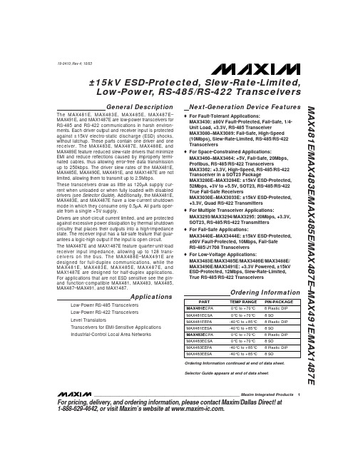
元器件交易网
MAX481E/MAX483E/MAX485E/MAX487E–MAX491E/MAX1487E
19-0410; Rev 4; 10/03
±15kV ESD-Protected, Slew-Rate-Limited, Low-Power, RS-485/RS-422 Transceivers
Ordering Information
PART MAX481ECPA MAX481ECSA MAX481EEPA MAX481EESA MAX483ECPA MAX483ECSA MAX483EEPA MAX483EESA
TEMP RANGE 0°C to +70°C 0°C to +70°C -40°C to +85°C -40°C to +85°C 0°C to +70°C 0°C to +70°C -40°C to +85°C -40°C to +85°C
- 1、下载文档前请自行甄别文档内容的完整性,平台不提供额外的编辑、内容补充、找答案等附加服务。
- 2、"仅部分预览"的文档,不可在线预览部分如存在完整性等问题,可反馈申请退款(可完整预览的文档不适用该条件!)。
- 3、如文档侵犯您的权益,请联系客服反馈,我们会尽快为您处理(人工客服工作时间:9:00-18:30)。
General DescriptionThe MAX481E, MAX483E, MAX485E, MAX487E–MAX491E, and MAX1487E are low-power transceivers for RS-485 and RS-422 communications in harsh environ-ments. Each driver output and receiver input is protected against ±15kV electro-static discharge (ESD) shocks,without latchup. These parts contain one driver and one receiver. The MAX483E, MAX487E, MAX488E, and MAX489E feature reduced slew-rate drivers that minimize EMI and reduce reflections caused by improperly termi-nated cables, thus allowing error-free data transmission up to 250kbps. The driver slew rates of the MAX481E,MAX485E, MAX490E, MAX491E, and MAX1487E are not limited, allowing them to transmit up to 2.5Mbps.These transceivers draw as little as 120µA supply cur-rent when unloaded or when fully loaded with disabled drivers (see Selector Guide ). Additionally, the MAX481E,MAX483E, and MAX487E have a low-current shutdown mode in which they consume only 0.5µA. All parts oper-ate from a single +5V supply.Drivers are short-circuit current limited, and are protected against excessive power dissipation by thermal shutdown circuitry that places their outputs into a high-impedance state. The receiver input has a fail-safe feature that guar-antees a logic-high output if the input is open circuit.The MAX487E and MAX1487E feature quarter-unit-load receiver input impedance, allowing up to 128 trans-ceivers on the bus. The MAX488E–MAX491E are designed for full-duplex communications, while the MAX481E, MAX483E, MAX485E, MAX487E, and MAX1487E are designed for half-duplex applications.For applications that are not ESD sensitive see the pin-and function-compatible MAX481, MAX483, MAX485,MAX487–MAX491, and MAX1487.ApplicationsLow-Power RS-485 Transceivers Low-Power RS-422 Transceivers Level TranslatorsTransceivers for EMI-Sensitive Applications Industrial-Control Local Area NetworksNext-Generation Device Features♦For Fault-Tolerant Applications:MAX3430: ±80V Fault-Protected, Fail-Safe, 1/4-Unit Load, +3.3V, RS-485 TransceiverMAX3080–MAX3089: Fail-Safe, High-Speed (10Mbps), Slew-Rate-Limited, RS-485/RS-422Transceivers ♦For Space-Constrained Applications:MAX3460–MAX3464: +5V, Fail-Safe, 20Mbps,Profibus, RS-485/RS-422 TransceiversMAX3362: +3.3V, High-Speed, RS-485/RS-422Transceiver in a SOT23 PackageMAX3280E–MAX3284E: ±15kV ESD-Protected,52Mbps, +3V to +5.5V, SOT23, RS-485/RS-422True Fail-Safe ReceiversMAX3030E–MAX3033E: ±15kV ESD-Protected,+3.3V, Quad RS-422 Transmitters ♦For Multiple Transceiver Applications:MAX3293/MAX3294/MAX3295: 20Mbps, +3.3V,SOT23, RS-485/RS-422 Transmitters ♦For Fail-Safe Applications:MAX3440E–MAX3444E: ±15kV ESD-Protected,±60V Fault-Protected, 10Mbps, Fail-Safe RS-485/J1708 Transceivers ♦For Low-Voltage Applications:MAX3483E/MAX3485E/MAX3486E/MAX3488E/MAX3490E/MAX3491E: +3.3V Powered, ±15kV ESD-Protected, 12Mbps, Slew-Rate-Limited, True RS-485/RS-422 TransceiversMAX481E/MAX483E/MAX485E/MAX487E–MAX491E/MAX1487E±15kV ESD-Protected, Slew-Rate-Limited, Low-Power, RS-485/RS-422 Transceivers________________________________________________________________Maxim Integrated Products 1Ordering Information19-0410; Rev 4; 10/03For pricing, delivery, and ordering information,please contact Maxim/Dallas Direct!at 1-888-629-4642, or visit Maxim’s website at .Ordering Information continued at end of data sheet.Selector Guide appears at end of data sheet .M A X 481E /M A X 483E /M A X 485E /M A X 487E –M A X 491E /M A X 1487E±15kV ESD-Protected, Slew-Rate-Limited,Low-Power, RS-485/RS-422 Transceivers2_______________________________________________________________________________________Supply Voltage (V CC ) (12V)Control Input Voltage (–R —E –, DE)...................-0.5V to (V CC + 0.5V)Driver Input Voltage (DI).............................-0.5V to (V CC + 0.5V)Driver Output Voltage (Y, Z; A, B)..........................-8V to +12.5V Receiver Input Voltage (A, B).................................-8V to +12.5V Receiver Output Voltage (RO)....................-0.5V to (V CC + 0.5V)Continuous Power Dissipation (T A = +70°C)8-Pin Plastic DIP (derate 9.09mW/°C above +70°C)....727mW14-Pin Plastic DIP (derate 10.00mW/°C above +70°C)..800mW 8-Pin SO (derate 5.88mW/°C above +70°C).................471mW 14-Pin SO (derate 8.33mW/°C above +70°C)...............667mW Operating Temperature RangesMAX4_ _C_ _/MAX1487EC_ A.............................0°C to +70°C MAX4__E_ _/MAX1487EE_ A...........................-40°C to +85°C Storage Temperature Range.............................-65°C to +160°C Lead Temperature (soldering, 10sec).............................+300°CDC ELECTRICAL CHARACTERISTICS(V CC = 5V ±5%, T A = T MIN to T MAX , unless otherwise noted.) (Notes 1, 2)Stresses beyond those listed under “Absolute Maximum Ratings” may cause permanent damage to the device. These are stress ratings only, and functional operation of the device at these or any other conditions beyond those indicated in the operational sections of the specifications is not implied. Exposure to absolute maximum rating conditions for extended periods may affect device reliability.ABSOLUTE MAXIMUM RATINGSPARAMETERSYMBOL MINTYPMAX UNITS Driver Common-Mode Output VoltageV OC 3V Change in Magnitude of Driver Differential Output Voltage for Complementary Output States ∆V OD 0.2V Change in Magnitude of Driver Common-Mode Output Voltage for Complementary Output States ∆V OD 0.2V Input High Voltage V IH 2.0V Input Low Voltage V IL 0.8V Input CurrentI IN1±2µADifferential Driver Output (no load)V OD15V 2V Differential Driver Output (with load)V OD2 1.551.0-0.8mA0.25mA -0.2Receiver Differential Threshold Voltage-0.20.2V Receiver Input Hysteresis ∆V TH 70mV Receiver Output High Voltage V OH 3.5Receiver Output Low Voltage V OL 0.4V Three-State (high impedance)Output Current at ReceiverI OZR±1µA 12k ΩCONDITIONSDE = 0V;V CC = 0V or 5.25V,all devices except MAX487E/MAX1487E R = 27Ωor 50Ω, Figure 8R = 27Ωor 50Ω, Figure 8R = 27Ωor 50Ω, Figure 8DE, DI, –R —E–MAX487E/MAX1487E,DE = 0V, V CC = 0V or 5.25VDE, DI, –R —E–DE, DI, –R —E–-7V ≤V CM ≤12V V CM = 0VI O = -4mA, V ID = 200mV I O = 4mA, V ID = -200mV R = 50Ω(RS-422)0.4V ≤V O ≤2.4VR = 27Ω(RS-485), Figure 8-7V ≤V CM ≤12V, all devices except MAX487E/MAX1487EReceiver Input Resistance R IN-7V ≤V CM ≤12V, MAX487E/MAX1487E48k ΩV TH I IN2Input Current (A, B)V IN = 12V V IN = -7V V IN = 12V V IN = -7VVMAX481E/MAX483E/MAX485E/MAX487E–MAX491E/MAX1487E±15kV ESD-Protected, Slew-Rate-Limited,Low-Power, RS-485/RS-422 TransceiversSWITCHING CHARACTERISTICS—MAX481E/MAX485E, MAX490E/MAX491E, MAX1487EDC ELECTRICAL CHARACTERISTICS (continued)(V CC = 5V ±5%, T A = T MIN to T MAX , unless otherwise noted.) (Notes 1, 2)M A X 481E /M A X 483E /M A X 485E /M A X 487E –M A X 491E /M A X 1487E±15kV ESD-Protected, Slew-Rate-Limited,Low-Power, RS-485/RS-422 Transceivers4_______________________________________________________________________________________SWITCHING CHARACTERISTICS—MAX483E, MAX487E/MAX488E/MAX489E(V CC = 5V ±5%, T A = T MIN to T MAX , unless otherwise noted.) (Notes 1, 2)SWITCHING CHARACTERISTICS—MAX481E/MAX485E, MAX490E/MAX491E, MAX1487E(continued)(V CC = 5V ±5%, T A = T MIN to T MAX , unless otherwise noted.) (Notes 1, 2)2251000Figures 11 and 13, C L = 100pF, S2 closed Figures 11 and 13, C L = 100pF, S1 closed Figures 9 and 15, C L = 15pF, S2 closed,A - B = 2VCONDITIONSns 45100t ZH(SHDN)Driver Enable from Shutdown toOutput High (MAX481E)nsFigures 9 and 15, C L = 15pF, S1 closed,B - A = 2Vt ZL(SHDN)Receiver Enable from Shutdownto Output Low (MAX481E)ns 45100t ZL(SHDN)Driver Enable from Shutdown toOutput Low (MAX481E)ns 2251000t ZH(SHDN)Receiver Enable from Shutdownto Output High (MAX481E)UNITS MINTYP MAX SYMBOLPARAMETERt PLH t SKEW Figures 10 and 12, R DIFF = 54Ω,C L1= C L2= 100pFt PHL Figures 10 and 12, R DIFF = 54Ω,C L1= C L2= 100pFDriver Input to Output Driver Output Skew to Output ns 20800ns ns 2000MAX483E/MAX487E, Figures 11 and 13,C L = 100pF, S2 closedt ZH(SHDN)Driver Enable from Shutdown to Output High2502000ns2500MAX483E/MAX487E, Figures 9 and 15,C L = 15pF, S1 closedt ZL(SHDN)Receiver Enable from Shutdown to Output Lowns 2500MAX483E/MAX487E, Figures 9 and 15,C L = 15pF, S2 closedt ZH(SHDN)Receiver Enable from Shutdown to Output Highns 2000MAX483E/MAX487E, Figures 11 and 13,C L = 100pF, S1 closedt ZL(SHDN)Driver Enable from Shutdown to Output Lowns 50200600MAX483E/MAX487E (Note 5)t SHDN Time to Shutdownt PHL t PLH , t PHL < 50% of data period Figures 9 and 15, C RL = 15pF, S2 closed Figures 9 and 15, C RL = 15pF, S1 closed Figures 9 and 15, C RL = 15pF, S2 closed Figures 9 and 15, C RL = 15pF, S1 closed Figures 11 and 13, C L = 15pF, S2 closed Figures 10 and 14, R DIFF = 54Ω,C L1= C L2= 100pFFigures 11 and 13, C L = 15pF, S1 closed Figures 11 and 13, C L = 100pF, S1 closed Figures 11 and 13, C L = 100pF, S2 closed CONDITIONSkbps 250f MAX 2508002000Maximum Data Rate ns 2550t HZ Receiver Disable Time from High ns 25080020002550t LZ Receiver Disable Time from Low ns 2550t ZH Receiver Enable to Output High ns 2550t ZL Receiver Enable to Output Low ns ns 1003003000t HZ t SKD Driver Disable Time from High I t PLH - t PHL I DifferentialReceiver SkewFigures 10 and 14, R DIFF = 54Ω,C L1= C L2= 100pFns 3003000t LZ Driver Disable Time from Low ns 2502000t ZL Driver Enable to Output Low ns Figures 10 and 12, R DIFF = 54Ω,C L1= C L2= 100pFns 2502000t R , t F 2502000Driver Rise or Fall Time ns t PLH Receiver Input to Output2502000t ZH Driver Enable to Output High UNITS MIN TYP MAX SYMBOL PARAMETERMAX481E/MAX483E/MAX485E/MAX487E–MAX491E/MAX1487E±15kV ESD-Protected, Slew-Rate-Limited,Low-Power, RS-485/RS-422 Transceivers_______________________________________________________________________________________505101520253035404550OUTPUT CURRENT vs.RECEIVER OUTPUT LOW VOLTAGEM A X 481E -01OUTPUT LOW VOLTAGE (V)O U T P U T C U R R E N T (m A )1.52.02.51.00.50.10.20.30.40.50.60.70.80.9-60-2060RECEIVER OUTPUT LOW VOLTAGEvs. TEMPERATURETEMPERATURE (°C)O U T P U T L O W V O L T A G E (V )20100-4040800-5-10-15-20-251.53.0OUTPUT CURRENT vs.RECEIVER OUTPUT HIGH VOLTAGEM A X 481E -02OUTPUT HIGH VOLTAGE (V)O U T P U T C U R R E N T (m A )5.04.54.02.02.53.53.03.23.43.63.84.04.24.44.64.8-60-2060RECEIVER OUTPUT HIGH VOLTAGEvs. TEMPERATURETEMPERATURE (°C)O U T P U T H I G H V O L T A G E (V )20100-4040800102030405060708090DRIVER OUTPUT CURRENT vs. DIFFERENTIAL OUTPUT VOLTAGEM A X 481E -05DIFFERENTIAL OUTPUT VOLTAGE (V)O U T P U T C U R R E N T (m A )1.52.0 2.53.0 3.54.0 4.51.00.50__________________________________________Typical Operating Characteristics(V CC = 5V, T A = +25°C, unless otherwise noted.)NOTES FOR ELECTRICAL/SWITCHING CHARACTERISTICSNote 1:All currents into device pins are positive; all currents out of device pins are negative. All voltages are referenced to deviceground unless otherwise specified.Note 2:All typical specifications are given for V CC = 5V and T A = +25°C.Note 3:Supply current specification is valid for loaded transmitters when DE = 0V.Note 4:Applies to peak current. See Typical Operating Characteristics.Note 5:The MAX481E/MAX483E/MAX487E are put into shutdown by bringing –R —E –high and DE low. If the inputs are in this state forless than 50ns, the parts are guaranteed not to enter shutdown. If the inputs are in this state for at least 600ns, the parts are guaranteed to have entered shutdown. See Low-Power Shutdown Mode section.M A X 481E /M A X 483E /M A X 485E /M A X 487E –M A X 491E /M A X 1487E±15kV ESD-Protected, Slew-Rate-Limited,Low-Power, RS-485/RS-422 Transceivers6___________________________________________________________________________________________________________________Typical Operating Characteristics (continued)(V CC = 5V, T A = +25°C, unless otherwise noted.)1.52.32.22.12.01.91.81.71.6-60-2060DRIVER DIFFERENTIAL OUTPUT VOLTAGE vs. TEMPERATURETEMPERATURE (°C)D I F FE R E N T I A L O U T P U T V O L T A G E (V )20100-404080020406080100120140OUTPUT CURRENT vs. DRIVER OUTPUT LOW VOLTAGEM A X 481E -07OUTPUT LOW VOLTAGE (V)O U T P U T C U R R E N T (m A )246810120-10-20-30-40-50-60-70-80-90-100-8-2OUTPUT CURRENT vs. DRIVER OUTPUT HIGH VOLTAGEM A X 481E -08OUTPUT HIGH VOLTAGE (V)O U T P U T C U R R E N T (m A )642-6-400100200300400500600-60-2060MAX481E/MAX485E/MAX490E/MAX491E SUPPLY CURRENT vs. TEMPERATURETEMPERATURE (°C)S U P P L Y C U R R E N T (µA )20100-4040800100200300400500600-60-2060MAX483E/MAX487E–MAX489E SUPPLY CURRENT vs. TEMPERATURETEMPERATURE (°C)S U P P L Y C U R R E N T (µA )20100-404080100200300400500600-60-2060MAX1487ESUPPLY CURRENT vs. TEMPERATURETEMPERATURE (°C)S U P P L Y C U R R E N T (µA )20100-404080±15kV ESD-Protected, Slew-Rate-Limited, Low-Power, RS-485/RS-422 Transceivers_______________________________________________________________________________________7MAX481E/MAX483E/MAX485E/MAX487E–MAX491E/MAX1487E______________________________________________________________Pin DescriptionM A X 481E /M A X 483E /M A X 485E /M A X 487E –M A X 491E /M A X 1487E±15kV ESD-Protected, Slew-Rate-Limited,Low-Power, RS-485/RS-422 Transceivers8_________________________________________________________________________________________________Function Tables (MAX481E/MAX483E/MAX485E/MAX487E/MAX1487E) Table 1. Transmitting__________Applications Information The MAX481E/MAX483E/MAX485E/MAX487E–MAX491E and MAX1487E are low-power transceivers for RS-485 and RS-422 communications. These “E” versions of the MAX481, MAX483, MAX485, MAX487–MAX491, and MAX1487 provide extra protection against ESD. The rugged MAX481E, MAX483E, MAX485E, MAX497E–MAX491E, and MAX1487E are intended for harsh envi-ronments where high-speed communication is important. These devices eliminate the need for transient suppres-sor diodes and the associated high capacitance loading. The standard (non-“E”) MAX481, MAX483, MAX485, MAX487–MAX491, and MAX1487 are recommended for applications where cost is critical.The MAX481E, MAX485E, MAX490E, MAX491E, and MAX1487E can transmit and receive at data rates up to 2.5Mbps, while the MAX483E, MAX487E, MAX488E, and MAX489E are specified for data rates up to 250kbps. The MAX488E–MAX491E are full-duplex transceivers, while the MAX481E, MAX483E, MAX487E, and MAX1487E are half-duplex. In addition, driver-enable (DE) and receiver-enable (RE) pins are included on the MAX481E, MAX483E, MAX485E, MAX487E, MAX489E, MAX491E, and MAX1487E. When disabled, the driver and receiver outputs are high impedance.±15kV ESD Protection As with all Maxim devices, ESD-protection structures are incorporated on all pins to protect against electro-static discharges encountered during handling and assembly. The driver outputs and receiver inputs have extra protection against static electricity. Maxim’s engi-neers developed state-of-the-art structures to protect these pins against ESD of ±15kV without damage. The ESD structures withstand high ESD in all states: normal operation, shutdown, and powered down. After an ESD event, Maxim’s MAX481E, MAX483E, MAX485E, MAX487E–MAX491E, and MAX1487E keep working without latchup.ESD protection can be tested in various ways; the transmitter outputs and receiver inputs of this product family are characterized for protection to ±15kV using the Human Body Model.Other ESD test methodologies include IEC10004-2 con-tact discharge and IEC1000-4-2 air-gap discharge (for-merly IEC801-2).ESD Test Conditions ESD performance depends on a variety of conditions. Contact Maxim for a reliability report that documents test set-up, test methodology, and test results.Human Body Model Figure 4 shows the Human Body Model, and Figure 5 shows the current waveform it generates when dis-charged into a low impedance. This model consists of a 100pF capacitor charged to the ESD voltage of inter-est, which is then discharged into the test device through a 1.5kΩresistor.IEC1000-4-2 The IEC1000-4-2 standard covers ESD testing and per-formance of finished equipment; it does not specifically refer to integrated circuits (Figure 6).MAX481E/MAX483E/MAX485E/MAX487E–MAX491E/MAX1487E±15kV ESD-Protected, Slew-Rate-Limited,Low-Power, RS-485/RS-422 Transceivers_______________________________________________________________________________________9M A X 481E /M A X 483E /M A X 485E /M A X 487E –M A X 491E /M A X 1487E±15kV ESD-Protected, Slew-Rate-Limited,Low-Power, RS-485/RS-422 Transceivers10______________________________________________________________________________________Figure 8. Driver DC Test LoadFigure 9. Receiver Timing Test LoadMAX481E/MAX483E/MAX485E/MAX487E–MAX491E/MAX1487E±15kV ESD-Protected, Slew-Rate-Limited,Low-Power, RS-485/RS-422 Transceivers______________________________________________________________________________________11Figure 10. Driver/Receiver Timing Test Circuit Figure 11. Driver Timing Test LoadFigure 12. Driver Propagation DelaysFigure 13. Driver Enable and Disable Times (except MAX488E and MAX490E)Figure 14. Receiver Propagation DelaysFigure 15. Receiver Enable and Disable Times (except MAX488E and MAX490E)M A X 481E /M A X 483E /M A X 485E /M A X 487E –M A X 491E /M A X 1487E±15kV ESD-Protected, Slew-Rate-Limited,Low-Power, RS-485/RS-422 Transceivers12______________________________________________________________________________________The major difference between tests done using the Human Body Model and IEC1000-4-2 is higher peak current in IEC1000-4-2, because series resistance is lower in the IEC1000-4-2 model. Hence, the ESD with-stand voltage measured to IEC1000-4-2 is generally lower than that measured using the Human Body Model. Figure 7 shows the current waveform for the 8kV IEC1000-4-2 ESD contact-discharge test.The air-gap test involves approaching the device with a charged probe. The contact-discharge method connects the probe to the device before the probe is energized.Machine ModelThe Machine Model for ESD tests all pins using a 200pF storage capacitor and zero discharge resis-tance. Its objective is to emulate the stress caused by contact that occurs with handling and assembly during manufacturing. Of course, all pins require this protec-tion during manufacturing—not just inputs and outputs.Therefore,after PC board assembly,the Machine Model is less relevant to I/O ports.MAX487E/MAX1487E:128 Transceivers on the BusThe 48k Ω, 1/4-unit-load receiver input impedance of the MAX487E and MAX1487E allows up to 128 transceivers on a bus, compared to the 1-unit load (12k Ωinput impedance) of standard RS-485 drivers (32 transceivers maximum). Any combination of MAX487E/MAX1487E and other RS-485 transceivers with a total of 32 unit loads or less can be put on the bus. The MAX481E,MAX483E, MAX485E, and MAX488E–MAX491E have standard 12k Ωreceiver input impedance.MAX483E/MAX487E/MAX488E/MAX489E:Reduced EMI and Reflections The MAX483E and MAX487E–MAX489E are slew-rate limited, minimizing EMI and reducing reflections caused by improperly terminated cables. Figure 16shows the driver output waveform and its Fourier analy-sis of a 150kHz signal transmitted by a MAX481E,MAX485E, MAX490E, MAX491E, or MAX1487E. High-frequency harmonics with large amplitudes are evident.Figure 17 shows the same information displayed for a MAX483E, MAX487E, MAX488E, or MAX489E transmit-ting under the same conditions. Figure 17’s high-fre-quency harmonics have much lower amplitudes, and the potential for EMI is significantly reduced.Low-Power Shutdown Mode (MAX481E/MAX483E/MAX487E)A low-power shutdown mode is initiated by bringing both RE high and DE low. The devices will not shut down unless both the driver and receiver are disabled.In shutdown, the devices typically draw only 0.5µA of supply current.RE and DE may be driven simultaneously; the parts are guaranteed not to enter shutdown if RE is high and DE is low for less than 50ns. If the inputs are in this state for at least 600ns, the parts are guaranteed to enter shutdown.For the MAX481E, MAX483E, and MAX487E, the t ZH and t ZL enable times assume the part was not in the low-power shutdown state (the MAX485E, MAX488E–MAX491E, and MAX1487E can not be shut down). The t ZH(SHDN)and t ZL(SHDN)enable times assume the parts were shut down (see Electrical Characteristics ).500kHz/div0Hz5MHz 10dB/div Figure 16. Driver Output Waveform and FFT Plot ofMAX485E/MAX490E/MAX491E/MAX1487E Transmitting a 150kHz Signal500kHz/div0Hz5MHz10dB/divFigure 17. Driver Output Waveform and FFT Plot ofMAX483E/MAX487E–MAX489E Transmitting a 150kHz SignalIt takes the drivers and receivers longer to become enabled from the low-power shutdown state (t ZH(SHDN), t ZL(SHDN)) than from the operating mode (t ZH, t ZL). (The parts are in operating mode if the RE, DE inputs equal a logical 0,1 or 1,1 or 0, 0.)Driver Output Protection Excessive output current and power dissipation caused by faults or by bus contention are prevented by two mechanisms. A foldback current limit on the output stage provides immediate protection against short circuits over the whole common-mode voltage range (see Typical Operating Characteristics). In addition, a thermal shut-down circuit forces the driver outputs into a high-imped-ance state if the die temperature rises excessively.Propagation Delay Many digital encoding schemes depend on the differ-ence between the driver and receiver propagation delay times. Typical propagation delays are shown in Figures 19–22 using Figure 18’s test circuit.The difference in receiver delay times, t PLH- t PHL, is typically under 13ns for the MAX481E, MAX485E, MAX490E, MAX491E, and MAX1487E, and is typically less than 100ns for the MAX483E and MAX487E–MAX489E.The driver skew times are typically 5ns (10ns max) for the MAX481E, MAX485E, MAX490E, MAX491E, and MAX1487E, and are typically 100ns (800ns max) for the MAX483E and MAX487E–MAX489E.Typical Applications The MAX481E, MAX483E, MAX485E, MAX487E–MAX491E, and MAX1487E transceivers are designed for bidirectional data communications on multipoint bus transmission lines. Figures 25 and 26 show typical net-work application circuits. These parts can also be used as line repeaters, with cable lengths longer than 4000 feet. To minimize reflections, the line should be terminated at both ends in its characteristic impedance, and stub lengths off the main line should be kept as short as possi-ble. The slew-rate-limited MAX483E and MAX487E–MAX489E are more tolerant of imperfect termination. Bypass the V CC pin with 0.1µF.Isolated RS-485 For isolated RS-485 applications, see the MAX253 and MAX1480 data sheets.Line Length vs. Data Rate The RS-485/RS-422 standard covers line lengths up to 4000 feet. Figures 23 and 24 show the system differen-tial voltage for the parts driving 4000 feet of 26AWG twisted-pair wire at 110kHz into 100Ωloads.Figure 18. Receiver Propagation Delay Test CircuitMAX481E/MAX483E/MAX485E/MAX487E–MAX491E/MAX1487E±15kV ESD-Protected, Slew-Rate-Limited,Low-Power, RS-485/RS-422 Transceivers ______________________________________________________________________________________13M A X 481E /M A X 483E /M A X 485E /M A X 487E –M A X 491E /M A X 1487E±15kV ESD-Protected, Slew-Rate-Limited,Low-Power, RS-485/RS-422 Transceivers14______________________________________________________________________________________25ns/div 5V/divRO B A500mV/div Figure 19. MAX481E/MAX485E/MAX490E/MAX1487E Receiver t PHL25ns/div5V/div ROBA500mV/divFigure 20. MAX481E/MAX485E/MAX490E/MAX491E/MAX1487E Receiver t PLH200ns/div 5V/divRO B A500mV/div Figure 21. MAX483E/MAX487E–MAX489E Receiver t PHL200ns/div5V/div ROBA500mV/divFigure 22. MAX483E/MAX487E–MAX489E Receiver t PLH2µs/div DO 0V0V5V5V -1V 0DIV A - V BFigure 23. MAX481E/MAX485E/MAX490E/MAX491E/MAX1487E System Differential Voltage at 110kHz Driving 4000ft of Cable 2µs/divDO0V0V 5V 5V -1V1V0DIV B - V AFigure 24. MAX483E/MAX1487E–MAX489E System Differential Voltage at 110kHz Driving 4000ft of CableMAX481E/MAX483E/MAX485E/MAX487E–MAX491E/MAX1487E±15kV ESD-Protected, Slew-Rate-Limited,Low-Power, RS-485/RS-422 Transceivers______________________________________________________________________________________15Figure 26. MAX488E–MAX491E Full-Duplex RS-485 NetworkFigure 25. MAX481E/MAX483E/MAX485E/MAX487E/MAX1487E Typical Half-Duplex RS-485 NetworkM A X 481E /M A X 483E /M A X 485E /M A X 487E –M A X 491E /M A X 1487E±15kV ESD-Protected, Slew-Rate-Limited, Low-Power, RS-485/RS-422 Transceivers Maxim cannot assume responsibility for use of any circuitry other than circuitry entirely embodied in a Maxim product. No circuit patent licenses are implied. Maxim reserves the right to change the circuitry and specifications without notice at any time.16____________________Maxim Integrated Products, 120 San Gabriel Drive, Sunnyvale, CA 94086 408-737-7600©2003 Maxim Integrated ProductsPrinted USAis a registered trademark of Maxim Integrated Products.Package InformationFor the latest package outline information, go to /packages .Ordering Information (continued)Selector GuideChip InformationTRANSISTOR COUNT: 295。